LM2655
2.5A High Efficiency Synchronous Switching Regulator
General Description
The LM2655 is a current-mode controlled PWM step-down
switching regulator. It has the unique ability to operate in
synchronous or asynchronous mode. This gives the
designer flexibility to choose between the high efficiency of
synchronous
operation,
or
the
low
solution
cost
of
asynchronous operation. Along with flexibility, the LM2655
offers high power density with the small footprint of a
TSSOP-16 package.
High efficiency (
>
90%) is obtained through the use of an
internal low ON-resistance (33m
) MOSFET, and an
external N-Channel MOSFET. This feature, together with its
low quiescent current, makes the LM2655 an ideal fit in
portable applications.
Integrated in the LM2655 are all the power, control, and drive
functions for asynchronous operation. In addition, a low-side
driver output allows easy synchronous operation. The IC
uses patented current sensing circuitry that eliminates the
external
current
sensing
resistor
required
by
other
current-mode DC-DC converters. A programmable soft-start
feature limits start up current surges and provides a means
of sequencing multiple power supplies.
Features
n
Ultra-high efficiency up to 96%
n
4V to 14V input voltage range
n
Internal high-side MOSFET with low R
DS(ON)
= 0.033
n
300 kHz fixed frequency internal oscillator
n
Low-side drive for synchronous operation
n
Guaranteed less than 12 µA shutdown current
n
Patented current sensing for current mode control
n
Programmable soft-start
n
Input undervoltage lockout
n
Output overvoltage shutdown protection
n
Output undervoltage shutdown protection
n
Thermal Shutdown
n
16-pin TSSOP package
Applications
n
Hard disk drives
n
Internet appliances
n
TFT monitors
n
Computer peripherals
n
Battery powered devices
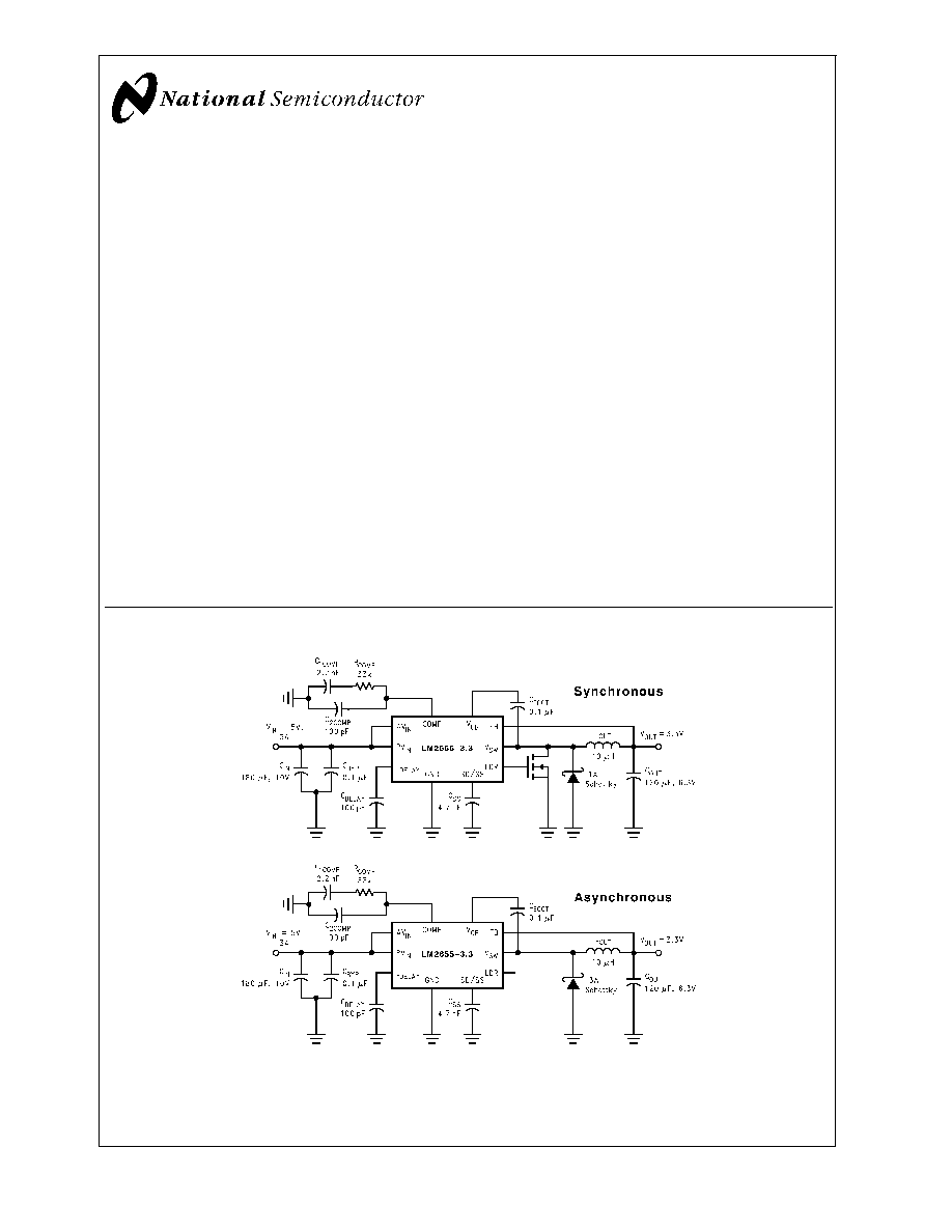
Typical Application
10128429
March 2001
LM2655
2.5A
High
Efficiency
Synchronous
Switching
Regulator
© 2001 National Semiconductor Corporation
DS101284
www.national.com
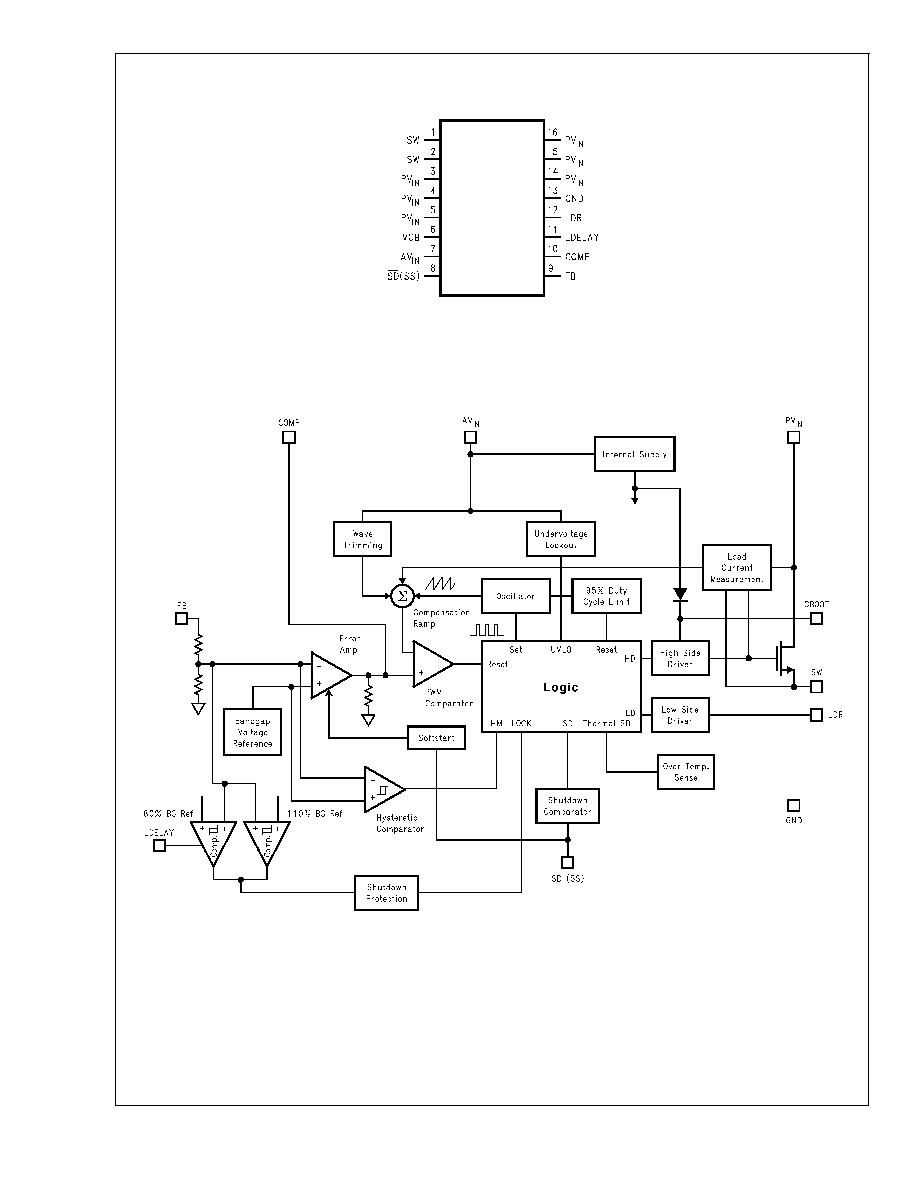
Connection Diagram
16-Lead TSSOP (MTC)
10128403
Top View
Order Number LM2655MTC-ADJ
See NS Package Number MTC16
Block Diagram
10128404
LM2655
www.national.com
2
Pin Description
Pin
Name
Function
1-2
SW
Switched-node connection, which is connected to the source of the internal high-side
MOSFET.
3-5
PV
IN
Main power supply input pin. Connected to the drain of the internal high-side MOSFET.
6
V
CB
Bootstrap capacitor connection for high-side gate drive.
7
AV
IN
Input voltage for control and drive circuits.
8
SD(SS)
Shutdown and Soft-start control pin. Pulling this pin below 0.3V shuts off the regulator. A
capacitor connected from this pin to ground provides a control ramp of the input current.
Do not drive this pin with an external source or erroneous operation may result.
9
FB
Output voltage feedback input. Connected to the output voltage.
10
COMP
Compensation network connection. Connected to the output of the voltage error amplifier.
11
L
DELAY
A capacitor between this pin to ground sets the delay from when the output voltage
reaches 80% of its nominal to when the undervoltage latch protection is enabled.
12
LDR
Low-side FET gate drive pin.
13
GND
Power ground.
14-16
PV
IN
Main power supply input pin. Connected to the drain of the internal high-side MOSFET.
Ordering Information
Supplied as 1000 units
Tape and Reel
Supplied as 3000 units,
Tape and Reel
LM2655MTC-3.3
LM2655MTCX-3.3
LM2655MTC-ADJ
LM2655MTCX-ADJ
LM2655
www.national.com
3
Absolute Maximum Ratings
(Note 1)
If Military/Aerospace specified devices are required,
please contact the National Semiconductor Sales
Office/Distributors for availability and specifications.
Supply Voltage (PV
IN
)
3.8V
V
IN
14V
Supply Voltage (AV
IN
)
4.0V
V
IN
14V
Feedback Pin Voltage
-0.4V
V
FB
5V
V
CB
Voltage, (Note 7)
7V
C
SS
Voltage
2.5V
Comp Voltage
2.5V
L
DELAY
Voltage
2.5V
LDR Voltage
5V
V
SW
, (Note 8)
14V
Power Dissipation (T
A
=25∞C),
(Note 2)
TSSOP-16 Package
JA
140∞C/W
Power Dissapation
893mW
Lead Temperature
Vapor Phase (60 sec.)
215∞C
Infrared (15 sec.)
220∞C
ESD Susceptibility(Note 3)
Human Body Model(Note 4)
1kV
Machine Model
200V
Operating Ratings
(Note 1)
Storage Temperature Range
-65∞C
T
J
+150∞C
Junction Temperature Range
-40∞C
T
J
+125∞C
LM2655-3.3 Electrical Characteristics
Specifications with standard typeface are for T
J
= 25∞C, and those in boldface type apply over full Operating Temperature
Range. V
IN
= 10V unless otherwise specified.
Symbol
Parameter
Conditions
Typical
(Note 5)
Limit
(Note 6)
Units
V
OUT
Output Voltage
I
LOAD
= 1.5 A
3.3
3.235/3.185
3.392/3.416
V
V(min)
V(max)
V
OUT
Output Voltage Line
Regulation
V
IN
= 5V to 14V
I
LOAD
= 1.5 A
0.5
0.7
%
%(max)
Output Voltage Load
Regulation
I
LOAD
= 100 mA to 2.5A
V
IN
=10V
0.6
1.7
%
%(max)
V
INUV
V
IN
Undervoltage Lockout
Threshold Voltage
Rising Edge
3.8
3.95
V
V(max)
V
UV_HYST
Hysteresis for the Input
Undervoltage Lockout
210
mV
I
CL
(Note 9)
Average Output Current
Limit
V
IN
= 5V
V
OUT
= 3.3V
3.3
LM2655-ADJ Electrical Characteristics
Specifications with standard typeface are for T
J
= 25∞C, and those in boldface type apply over full Operating Temperature
Range. V
IN
= 10V unless otherwise specified.
Symbol
Parameter
Conditions
Typical
(Note 5)
Limit
(Note 6)
Units
V
FB
Feedback Voltage
I
LOAD
= 1.5 A
1.238
1.208/1.181
1.260/1.267
V
V(min)
V(max)
V
OUT
Output Voltage Line
Regulation
V
IN
= 5V to 14V
I
LOAD
= 1.5 A
0.5
0.7
%
%(max)
Output Voltage Load
Regulation
I
LOAD
= 100 mA to 2.5A
V
IN
=10V
0.6
1.7
%
%(max)
V
INUV
V
IN
Undervoltage Lockout
Threshold Voltage
Rising Edge
3.8
3.95
V
V(max)
V
UV_HYST
Hysteresis for the Input
Undervoltage Lockout
210
mV
I
CL
(Note 9)
Average Output Current
Limit
V
IN
= 5V
V
OUT
= 3.3V
3.3
A
LM2655
www.national.com
4

All Output Voltage Versions Electrical Characteristics
Specifications with standard typeface are for T
J
= 25∞C, and those in boldface type apply over full Operating Temperature
Range. V
IN
= 10V unless otherwise specified.
Symbol
Parameter
Conditions
Typical
(Note 6)
Limit
(Note 5)
Units
I
Q
Quiescent Current
Shutdown Pin Floating (Device
On)
Device Not Switching
1.7
3
mA
mA(max)
I
QSD
Quiescent Current in
Shutdown Mode
Shutdown Pin Pulled Low
7
12/20
µA
µA(max)
R
DS(ON)
Switch ON Resistance
I
SWITCH
= 1.5A
33
80
m
m
(max)
R
SW(ON)
Switch On Resistance
(MOSFET ON Resistance +
Bonding Wire Resistance)
I
SWITCH
= 1.5A
72
m
I
L
Switch Leakage Current
5
nA
V
BOOT
Bootstrap Regulator Voltage
I
BOOT
= 1 mA
C
BOOT
=tbd
6.7
6.4
7.0
V
V(min)
V(max)
G
M
Error Amplifier
Transconductance
1250
µmho
A
V
Error Amplifier Voltage Gain
100
I
EA_SOURCE
Error Amplifier Source
Current
V
IN
= 4V, V
FB
= .9*V
OUT
, V
COMP
= 2V
40
32/10
µA
µA(min)
I
EA_SINK
Error Amplifier Sink Current
V
IN
= 4V, V
FB
= 1.1*V
OUT
, V
COMP
= 2V
80
53/30
µA
µA(min)
V
EAH
Error Amplifier Output Swing
Upper Limit
V
IN
= 4V, V
FB
= .9*V
OUT
, V
COMP
= 2V
2.70
2.50/2.40
V
V(min)
V
EAL
Error Amplifier Output Swing
Lower Limit
V
IN
= 4V, V
FB
= .9*V
OUT
, V
COMP
= 2V
1.25
1.35/1.50
V
V(max)
F
OSC
Oscillator Frequency
Measured at Switch Pin
V
IN
= 4V
300
280/255
330/345
kHz
kHz(min)
kHz(max)
D
MAX
Maximum Duty Cycle
V
IN
= 4V
95
92
%
%(min)
I
SS
Soft-Start Current
Voltage at the SS Pin = 1.4V
11
14
µA
µA(max)
V
OUTUV
V
OUT
Undervoltage Lockout
Threshold Voltage
81
76
84
%V
OUT
%V
OUT
(min)
%V
OUT
(max)
Hysteresis for V
OUTUV
5
%V
OUT
V
OUTOV
V
OUT
Overvoltage Lockout
Threshold Voltage
108
106
114
%V
OUT
%V
OUT
(min)
%V
OUT
(max)
Hysteresis for V
OUTOV
5
%V
OUT
I
LDELAY__
SOURCE
LDELAY Pin Source Current
5
µA
I
SHUTDOWN
Shutdown Pin Current
Shutdown Pin Pulled Low
2.2
3.7/4.0
µA
µA(max)
V
SHUTDOWN
Shutdown Pin Threshold
Voltage
Rising Edge
0.6
0.25
0.9
V
V(min)
V(max)
T
SD
Thermal Shutdown
Temperature
165
∞C
LM2655
www.national.com
5