LM2662/LM2663
Switched Capacitor Voltage Converter
General Description
The LM2662/LM2663 CMOS charge-pump voltage con-
verter inverts a positive voltage in the range of 1.5V to 5.5V
to the corresponding negative voltage. The LM2662/LM2663
uses two low cost capacitors to provide 200 mA of output
current without the cost, size, and EMI related to inductor
based converters. With an operating current of only 300 µA
and operating efficiency greater than 90% at most loads, the
LM2662/LM2663 provides ideal performance for battery
powered systems. The LM2662/LM2663 may also be used
as a positive voltage doubler.
The oscillator frequency can be lowered by adding an exter-
nal capacitor to the OSC pin. Also, the OSC pin may be used
to drive the LM2662/LM2663 with an external clock. For
LM2662, a frequency control (FC) pin selects the oscillator
frequency of 20 kHz or 150 kHz. For LM2663, an external
shutdown (SD) pin replaces the FC pin. The SD pin can be
used to disable the device and reduce the quiescent current
to 10 µA. The oscillator frequency for LM2663 is 150 kHz.
Features
n
Inverts or doubles input supply voltage
n
Narrow SO-8 Package
n
3.5
typical output resistance
n
86% typical conversion efficiency at 200 mA
n
(LM2662) selectable oscillator
frequency: 20 kHz/150 kHz
n
(LM2663) low current shutdown mode
Applications
n
Laptop computers
n
Cellular phones
n
Medical instruments
n
Operational amplifier power supplies
n
Interface power supplies
n
Handheld instruments
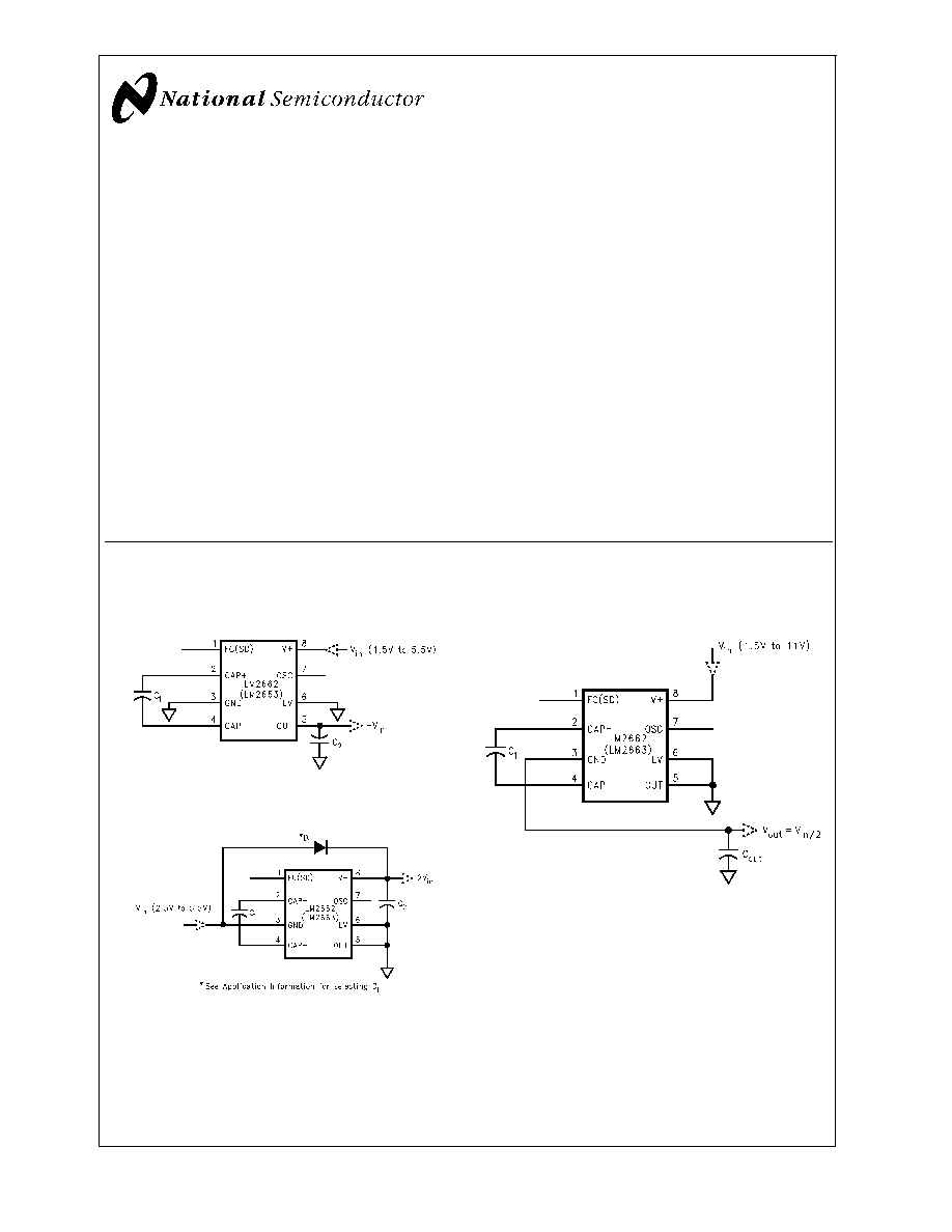
Basic Application Circuits
Voltage Inverter
DS100003-1
Positive Voltage Doubler
DS100003-2
Splitting V
IN
in Half
DS100003-3
January 1999
LM2662/LM2663
Switched
Capacitor
V
oltage
Converter
© 2001 National Semiconductor Corporation
DS100003
www.national.com

Absolute Maximum Ratings
(Note 1)
If Military/Aerospace specified devices are required,
please contact the National Semiconductor Sales Office/
Distributors for availability and specifications.
Supply Voltage (V+ to GND, or GND to OUT)
6V
LV
(OUT - 0.3V) to (GND + 3V)
FC, OSC, SD
The least negative of (OUT - 0.3V)
or (V+ - 6V) to (V+ + 0.3V)
V+ and OUT Continuous Output Current
250 mA
Output Short-Circuit Duration to GND (Note 2)
1 sec.
Power Dissipation (T
A
= 25∞C) (Note 3)
735 mW
T
J
Max (Note 3)
150∞C
JA
(Note 3)
170∞C/W
Operating Junction Temperature
Range
-40∞C to +85∞C
Storage Temperature Range
-65∞C to +150∞C
Lead Temperature (Soldering, 10 seconds)
300∞C
ESD Rating
2 kV
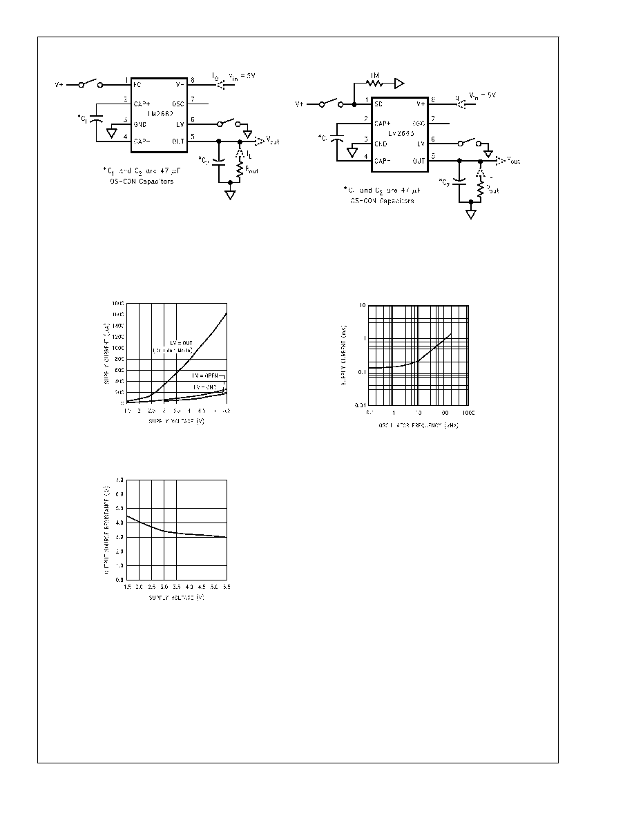
Electrical Characteristics
Limits in standard typeface are for T
J
= 25∞C, and limits in boldface type apply over the full operating temperature range. Un-
less otherwise specified: V+ = 5V, FC = Open, C
1
= C
2
= 47 µF.(Note 4)
Symbol
Parameter
Condition
Min
Typ
Max
Units
V+
Supply Voltage
R
L
= 1k
Inverter, LV = Open
3.5
5.5
Inverter, LV = GND
1.5
5.5
V
Doubler, LV = OUT
2.5
5.5
I
Q
Supply Current
No Load
FC = V+ (LM2662)
1.3
4
mA
LV = Open
SD = Ground (LM2663)
FC = Open
0.3
0.8
I
SD
Shutdown Supply Current
10
µA
(LM2663)
V
SD
Shutdown Pin Input Voltage
Shutdown Mode
2.0
(Note 5)
V
(LM2663)
Normal Operation
0.3
I
L
Output Current
200
mA
R
OUT
Output Resistance (Note 6)
I
L
= 200 mA
3.5
7
f
OSC
Oscillator Frequency (Note 7)
OSC = Open
FC = Open
7
20
kHz
FC = V+
55
150
f
SW
Switching Frequency (Note 8)
OSC = Open
FC = Open
3.5
10
kHz
FC = V+
27.5
75
I
OSC
OSC Input Current
FC = Open
±
2
µA
FC = V+
±
10
P
EFF
Power Efficiency
R
L
(500) between V
+
and OUT
90
96
%
I
L
= 200 mA to GND
86
V
OEFF
Voltage Conversion Efficiency
No Load
99
99.96
%
Note 1: Absolute maximum ratings indicate limits beyond which damage to the device may occur. Electrical specifications do not apply when operating the device
beyond its rated operating conditions.
Note 2: OUT may be shorted to GND for one second without damage. However, shorting OUT to V+ may damage the device and should be avoided. Also, for
temperatures above 85∞C, OUT must not be shorted to GND or V+, or device may be damaged.
Note 3: The maximum allowable power dissipation is calculated by using P
DMax
= (T
JMax
- T
A
)/
JA
, where T
JMax
is the maximum junction temperature, T
A
is the
ambient temperature, and
JA
is the junction-to-ambient thermal resistance of the specified package.
Note 4: In the test circuit, capacitors C
1
and C
2
are 47 µF, 0.2
maximum ESR capacitors. Capacitors with higher ESR will increase output resistance, reduce
output voltage and efficiency.
Note 5: In doubling mode, when V
out
>
5V, minimum input high for shutdown equals V
out
- 3V.
Note 6: Specified output resistance includes internal switch resistance and capacitor ESR.
Note 7: For LM2663, the oscillator frequency is 150 kHz.
Note 8: The output switches operate at one half of the oscillator frequency, f
OSC
= 2f
SW
.
LM2662/LM2663
www.national.com
2
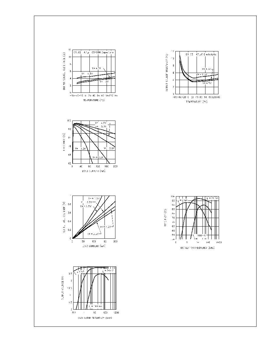
Typical Performance Characteristics
(Circuit of
Figure 1) (Continued)
Output Source
Resistance vs
Temperature
DS100003-40
Output Source
Resistance vs
Temperature
DS100003-41
Efficiency vs Load
Current
DS100003-42
Output Voltage Drop
vs Load Current
DS100003-43
Efficiency vs
Oscillator Frequency
DS100003-44
Output Voltage vs
Oscillator Frequency
DS100003-45
LM2662/LM2663
www.national.com
4

Typical Performance Characteristics
(Circuit of
Figure 1) (Continued)
Oscillator Frequency
vs External
Capacitance
DS100003-46
Oscillator Frequency
vs Supply Voltage
DS100003-47
Oscillator Frequency
vs Supply Voltage
DS100003-48
Oscillator Frequency
vs Temperature
DS100003-49
Oscillator Frequency
vs Temperature
DS100003-50
Shutdown Supply
Current vs
Temperature
(LM2663 Only)
DS100003-51
LM2662/LM2663
www.national.com
5