 | –≠–ª–µ–∫—Ç—Ä–æ–Ω–Ω—ã–π –∫–æ–º–ø–æ–Ω–µ–Ω—Ç: LM2681M6X | –°–∫–∞—á–∞—Ç—å:  PDF PDF  ZIP ZIP |
LM2681
Switched Capacitor Voltage Converter
General Description
The LM2681 CMOS charge-pump voltage converter oper-
ates as a voltage doubler for an input voltage in the range of
+2.5V to +5.5V. Two low cost capacitors and a diode
(needed during start-up) is used in this circuit to provide up
to 20 mA of output current. The LM2681 can also work as a
voltage divider to split a voltage in the range of +1.8V to
+11V in half.
The LM2681 operates at 160 kHz oscillator frequency to re-
duce output resistance and voltage ripple. With an operating
current of only 550 µA (operating efficiency greater than 90%
with most loads) the LM2681 provides ideal performance for
battery powered systems. The device is in SOT-23-6 pack-
age.
Features
n
Doubles or Splits Input Supply Voltage
n
SOT23-6 Package
n
15
Typical Output Impedance
n
90% Typical Conversion Efficiency at 20 mA
Applications
n
Cellular Phones
n
Pagers
n
PDAs
n
Operational Amplifier Power Suppliers
n
Interface Power Suppliers
n
Handheld Instruments
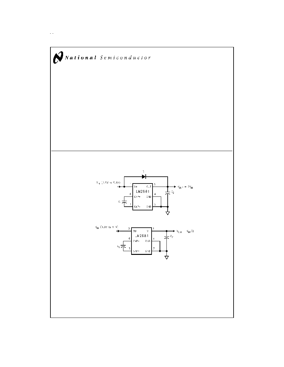
Basic Application Circuits
Voltage Doubler
DS100965-1
Splitting V
in
in Half
DS100965-2
March 1999
LM2681
Switched
Capacitor
V
oltage
Converter
© 1999 National Semiconductor Corporation
DS100965
www.national.com
Absolute Maximum Ratings
(Note 1)
If Military/Aerospace specified devices are required,
please contact the National Semiconductor Sales Office/
Distributors for availability and specifications.
Supply Voltage (V+ to GND, or GND to OUT)
5.8V
V+ and OUT Continuous Output Current
30 mA
Output Short-Circuit Duration to GND (Note 2)
1 sec.
Continuous Power
Dissipation (T
A
= 25∞C)(Note 3)
600 mW
T
JMax
(Note 3)
150∞C
JA
(Note 3)
210∞C/W
Operating Junction Temperature
Range
-40∞ to 85∞C
Storage Temperature Range
-65∞C to +150∞C
Lead Temp. (Soldering, 10 seconds)
300∞C
ESD Rating
2kV
Electrical Characteristics
Limits in standard typeface are for T
J
= 25∞C, and limits in boldface type apply over the full operating temperature range. Un-
less otherwise specified: V+ = 5V, C
1
= C
2
= 3.3 µF. (Note 4)
Symbol
Parameter
Condition
Min
Typ
Max
Units
V+
Supply Voltage
2.5
5.5
V
I
Q
Supply Current
No Load
550
1000
µA
I
L
Output Current
20
mA
R
SW
Sum of the R
ds(on)
of the four
internal MOSFET switches
I
L
= 20 mA
8
16
R
OUT
Output Resistance (Note 5)
I
L
= 20 mA
15
40
f
OSC
Oscillator Frequency
(Note 6)
80
160
kHz
f
SW
Switching Frequency
(Note 6)
40
80
kHz
P
EFF
Power Efficiency
R
L
(1.0k) between GND and
OUT
86
93
%
I
L
= 20 mA to GND
90
V
OEFF
Voltage Conversion Efficiency
No Load
99
99.96
%
Note 1: Absolute maximum ratings indicate limits beyond which damage to the device may occur. Electrical specifications do not apply when operating the device
beyond its rated operating conditions.
Note 2: OUT may be shorted to GND for one second without damage. However, shorting OUT to V+ may damage the device and should be avoided. Also, for tem-
peratures above 85∞C, OUT must not be shorted to GND or V+, or device may be damaged.
Note 3: The maximum allowable power dissipation is calculated by using P
DMax
= (T
JMax
- T
A
)/
JA
, where T
JMax
is the maximum junction temperature, T
A
is the
ambient temperature, and
JA
is the junction-to-ambient thermal resistance of the specified package.
Note 4: In the test circuit, capacitors C
1
and C
2
are 3.3 µF, 0.3
maximum ESR capacitors. Capacitors with higher ESR will increase output resistance, reduce output
voltage and efficiency.
Note 5: Specified output resistance includes internal switch resistance and capacitor ESR. See the details in the application information for positive voltage doubler.
Note 6: The output switches operate at one half of the oscillator frequency, f
OSC
= 2f
SW
.
www.national.com
2
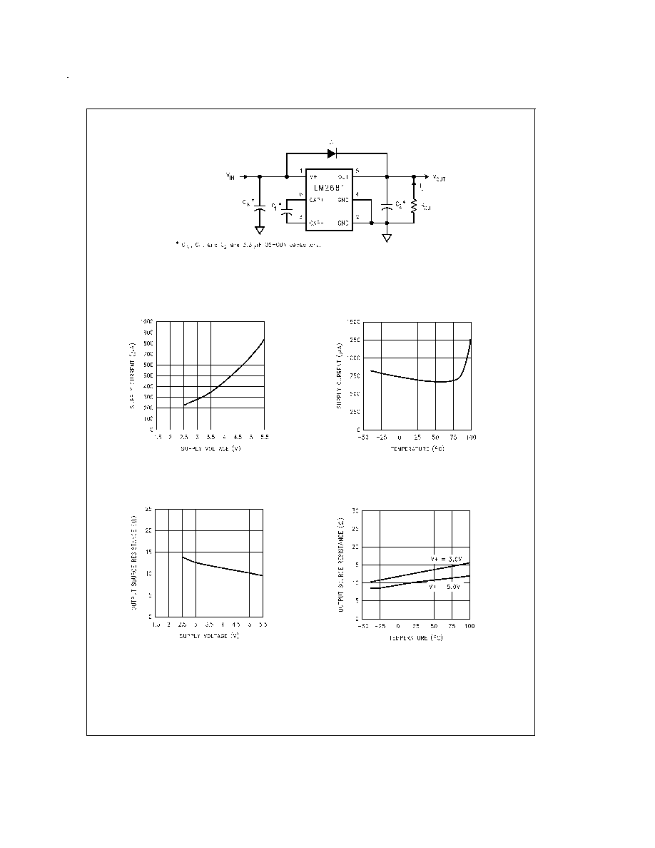
Test Circuit
Typical Performance Characteristics
(Circuit of Figure 1, V+ = 5V unless otherwise specified)
DS100965-3
FIGURE 1. LM2681 Test Circuit
Supply Current vs
Supply Voltage
DS100965-4
Supply Current vs
Temperature
DS100965-5
Output Source
Resistance vs Supply
Voltage
DS100965-6
Output Source
Resistance vs
Temperature
DS100965-7
www.national.com
3
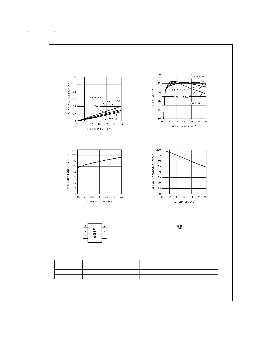
Typical Performance Characteristics
(Circuit of Figure 1, V+ = 5V unless otherwise
specified) (Continued)
Connection Diagram
Ordering Information
Order Number
Package
Number
Package
Marking
Supplied as
LM2681M6
MA06A
S10A (Note 7)
Tape and Reel (250 units/rail)
LM2681M6X
MA06A
S10A (Note 7)
Tape and Reel (3000 units/rail)
Note 7: The first letter
S
identifies the part as a switched capacitor converter. The next two numbers are the device number. The fourth letter
A
indicates the
grade. Only one grade is available. Larger quantity reels are available upon request.
Output Voltage Drop
vs Load Current
DS100965-8
Efficiency vs
Load Current
DS100965-9
Oscillator Frequency vs
Supply Voltage
DS100965-10
Oscillator Frequency vs
Temperature
DS100965-11
6-Lead SOT (M6)
DS100965-13
Top View With Package Marking
DS100965-22
Actual Size
www.national.com
4
Pin Description
Pin
Name
Function
Voltage Doubler
Voltage Split
1
V+
Power supply positive voltage input
Positive voltage output
2
GND
Power supply ground input
Same as doubler
3
CAP-
Connect this pin to the negative terminal of the
charge-pump capacitor
Same as doubler
4
GND
Power supply ground input
Same as doubler
5
OUT
Positive voltage output
Power supply positive voltage
input
6
CAP+
Connect this pin to the positive terminal of the
charge-pump capacitor
Same as doubler
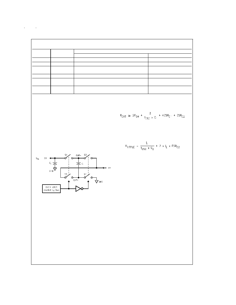
Circuit Description
The LM2681 contains four large CMOS switches which are
switched in a sequence to double the input supply voltage.
Energy transfer and storage are provided by external capaci-
tors. Figure 2 illustrates the voltage conversion scheme.
When S
2
and S
4
are closed, C
1
charges to the supply volt-
age V+. During this time interval, switches S
1
and S
3
are
open. In the next time interval, S
2
and S
4
are open; at the
same time, S
1
and S
3
are closed, the sum of the input volt-
age V+ and the voltage across C
1
gives the 2V+ output volt-
age when there is no load. The output voltage drop when a
load is added is determined by the parasitic resistance (R
d-
s(on)
of the MOSFET switches and the ESR of the capacitors)
and the charge transfer loss between capacitors. Details will
be discussed in the following application information section.
Application Information
Positive Voltage Doubler
The main application of the LM2681 is to double the input
voltage. The range of the input supply voltage is 2.5V to
5.5V.
The output characteristics of this circuit can be approximated
by an ideal voltage source in series with a resistance. The
voltage source equals 2V+. The output resistance R
out
is a
function of the ON resistance of the internal MOSFET
switches, the oscillator frequency, the capacitance and ESR
of C
1
and C
2
. Since the switching current charging and dis-
charging C
1
is approximately twice as the output current, the
effect of the ESR of the pumping capacitor C
1
will be multi-
plied by four in the output resistance. The output capacitor
C
2
is charging and discharging at a current approximately
equal to the output current, therefore, its ESR only counts
once in the output resistance. A good approximation of R
out
is:
where R
SW
is the sum of the ON resistance of the internal
MOSFET switches shown in Figure 2.
The peak-to-peak output voltage ripple is determined by the
oscillator frequency, the capacitance and ESR of the output
capacitor C
2
:
High capacitance, low ESR capacitors can reduce both the
output reslistance and the voltage ripple.
The Schottky diode D
1
is only needed for start-up. The inter-
nal oscillator circuit uses the OUT pin and the GND pin. Volt-
age across OUT and GND must be larger than 1.8V to insure
the operation of the oscillator. During start-up, D
1
is used to
charge up the voltage at the OUT pin to start the oscillator;
also, it protects the device from turning-on its own parasitic
diode and potentially latching-up. Therefore, the Schottky di-
ode D
1
should have enough current carrying capability to
charge the output capacitor at start-up, as well as a low for-
ward voltage to prevent the internal parasitic diode from
turning-on. A Schottky diode like 1N5817 can be used for
most applications. If the input voltage ramp is less than 10V/
ms, a smaller Schottky diode like MBR0520LT1 can be used
to reduce the circuit size.
Split V+ in Half
Another interesting application shown in the Basic Applica-
tion Circuits is using the LM2681 as a precision voltage di-
vider. . This circuit can be derived from the voltage doubler
by switching the input and output connections. In the voltage
divider, the input voltage applies across the OUT pin and the
GND pin (which are the power rails for the internal oscillator),
therefore no start-up diode is needed. Also, since the
off-voltage across each switch equals V
in
/2, the input voltage
can be raised to +11V.
DS100965-14
FIGURE 2. Voltage Doubling Principle
www.national.com
5