 | –≠–ª–µ–∫—Ç—Ä–æ–Ω–Ω—ã–π –∫–æ–º–ø–æ–Ω–µ–Ω—Ç: LM2687MM | –°–∫–∞—á–∞—Ç—å:  PDF PDF  ZIP ZIP |
LM2687
Low Noise Regulated Switched Capacitor Voltage
Inverter
General Description
The LM2687 CMOS Negative Regulated Switched Capacitor
Voltage Inverter delivers a very low noise adjustable output
for an input voltage in the range of +2.7V to +5.5V. Four low
cost capacitors are used in this circuit to provide up to 10mA
of output current. The regulated output for the LM2687 is ad-
justable between -1.5V and -5.2V. The LM2687 operates at
100 kHz (typical) switching frequency to reduce output resis-
tance and voltage ripple. With an operating current of only
500 µA (charge pump power efficiency greater than 90%
with most loads) and 0.05 µA typical shutdown current, the
LM2687 provides ideal performance for cellular phone power
amplifier bias and other low current, low noise negative volt-
age needs. The device comes in a small 8-pin MSOP pack-
age.
Features
n
Inverts and regulates the input supply voltage
n
Small MSOP-8 package
n
91% typical charge pump power efficiency at 10mA
n
Low output ripple (1mV typical)
n
Shutdown lowers Quiescent current to 0.05 µA (typical)
Applications
n
Wireless Communication Systems
n
Cellular Phone Power Amplifier Biasing
n
Interface Power Supplies
n
Handheld Instrumentation
n
Laptop Computers and PDA's
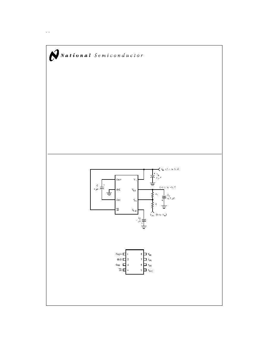
Typical Application Circuit
Connection Diagram
DS101180-1
8-Pin MSOP
DS101180-2
August 1999
LM2687
Low
Noise
Regulated
Switched
Capacitor
V
oltage
Inverter
© 1999 National Semiconductor Corporation
DS101180
www.national.com
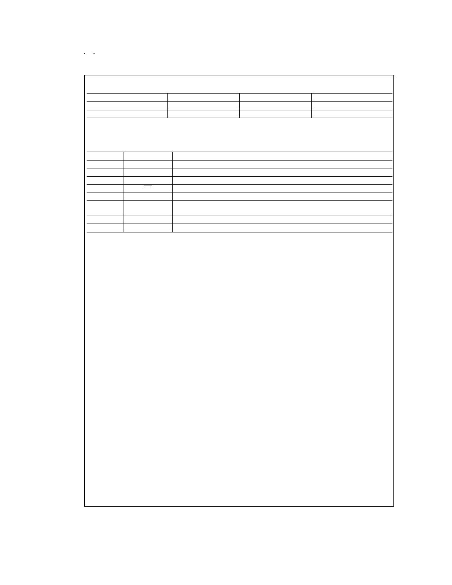
Ordering Information
Device Order Number
Package Number
Package Marking
*
Supplies As
LM2687MM
MUA08A
S12A
Tape and Reel (1000 units/reel)
LM2687MMX
MUA08A
S12A
Tape and Reel (3500 units/reel)
Note:
*
The small physical size of the MSOP-8 package does not allow for the full part number marking. Devices will be marked with the designation shown in the
column Package Marking.
Pin Description
Pin No.
Name
Function
1
Cap+
Positive terminal for C
1
.
2
GND
Ground.
3
Cap-
Negative terminal for C
1
.
4
SD
Active low, logic-level shutdown input.
5
V
NEG
Negative unregulated output voltage.
6
V
FB
Feedback input. Connect V
FB
to an external resistor divider between V
OUT
and a positive
adjust voltage V
ADJ
(0
V
ADJ
V
IN
). DO NOT leave unconnected.
7
V
OUT
Regulated negative output voltage.
8
V
IN
Positive power supply input.
www.national.com
2
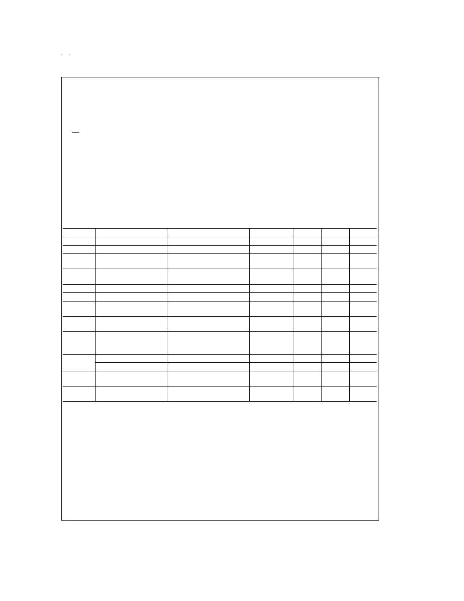
Absolute Maximum Ratings
(Note 1)
If Military/Aerospace specified devices are required,
please contact the National Semiconductor Sales Office/
Distributors for availability and specifications.
Supply Voltage (V
IN
to GND or
GND to OUT)
+ 5.8V
SD
(GND - 0.3V) to
(V
IN
+ 0.3V)
V
NEG
and V
OUT
Continuous Output
Current
10mA
V
OUT
Short-Circuit Duration to GND
(Note 2)
1 sec.
Continuous Power Dissipation (T
A
= 25∞C) (Note 3)
600mW
T
JMAX
(Note 3)
150∞C
JA
(Note 3)
250∞C/W
Operating Input Voltage Range
2.7V to 5.5V
Operating Output Current Range
0mA to 10mA
Operating Ambient
-40∞C to 85∞C
Temp. Range
Operating Junction Temp. Range
-40∞C to 110∞C
Storage Temperature
-65∞C to 150∞C
Lead Temp. (Soldering, 10 sec.)
300∞C
ESD Rating (Note 4)
2kV
Electrical Characteristics
Limits with standard typeface apply for T
J
= 25∞C, and limits in boldface type apply over the full temperature range. Unless
otherwise specified V
IN
= 3.6V, C
1
= C
2
= 1µF, C
3
= 10µF.
Symbol
Parameter
Conditions
Min
Typ
Max
Units
I
Q
Supply Current
Open Circuit, No Load
500
950
µA
I
SD
Shutdown Supply Current
0.05
1
µA
F
SW
Switching Frequency
(Note 5)
2.7V
V
IN
.5.5V
V
IN
= 3.6V
50
60
110
105
180
170
kHz
POWER
Power Efficiency at V
NEG
I
L
= 3.6mA
I
L
= 10mA
94
91
%
T
START
Start Up time
(Note 6)
120
600
µs
R
NEG
Output Resistance to V
NEG
(Note 7)
30
V
R
Output Voltage Ripple
(Note 8)
I
L
=2.5mA, V
OUT
= -2.7V
I
L
= 10mA, V
OUT
= -3.8V
1
2
mV
V
FB
Feedback Pin Reference
Voltage
I
L
= 2.5mA (Note 9)
-1.25
-1.20
-1.15
V
V
OUT
Adjustable Output Voltage
5.5V
V
IN
2.7V, 2.5mA
I
L
5.5V
V
IN
3.0V, 10mA
I
L
0mA
- (V
IN
-0.3V)
- (V
IN
-1.2V)
V
Load Regulation
0 to 10mA, V
OUT
= - 2.4V
5
mV/mA
Line Regulation
5.5V
V
IN
2.7V, I
L
= 2.5mA
1
mV/V
V
IH
Shutdown Pin Input
Voltage High
5.5V
V
IN
2.7V
2.2
V
V
IL
Shutdown Pin Input
Voltage Low
5.5V
V
IN
2.7V
0.5
V
Note 1: Absolute Maximum Ratings indicate limits beyond which damage to the device may occur. Electrical specifications do not apply when operating the device
beyond its rated operating conditions.
Note 2: OUT may be shorted to GND for one second without damage. However, shorting OUT to V
IN
may damage the device and must be avoided. Also, for tem-
peratures above T
A
= 85∞C, OUT must not be shorted to GND or V
IN
or device may be damaged.
Note 3: The maximum power dissipation must be de-rated at elevated temperatures and is limited by T
JMAX
(maximum junction temperature), T
A
(ambient tempera-
ture) and
JA
(junction-to-ambient thermal resistance). The maximum power dissipation at any temperature is:
PDiss
MAX
= (T
JMAX
-- T
A
)/
JA
up to the value listed in the Absolute Maximum Ratings.
Note 4: Rating is for the human body model, a 100pF capacitor discharged through a 1.5 k
resistor into each pin.
Note 5: The output switches operate at one half the oscillator frequency, f
OSC
= 2f
SW
.
Note 6: All capacitors are 1µF.
Note 7: Current drawn from V
NEG
pin decreases power efficiency and will increase output voltage ripple.
Note 8: In the test circuit, capacitors C
1
and C
2
are 1µF, C
3
= 10µF, 0.30
maximum ESR capacitors. Capacitors with higher ESR will increase output resistance,
increase output voltage ripple, and reduce efficiency.
Note 9: The feedback resistors R1 and R2 are 200k
resistors.
www.national.com
3
Electrical Characteristics
(Continued)
Typical Performance Characteristics
Unless otherwise specified, T
A
= 25∞C, V
OUT
= -2.5V.
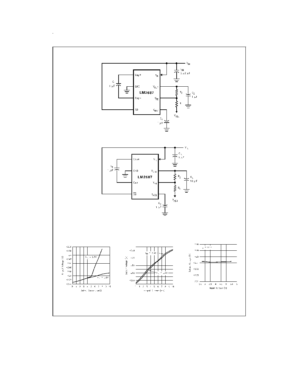
DS101180-21
FIGURE 1. Standard Application Circuit for Minimum Capacitance Values
DS101180-22
FIGURE 2. Standard Application Circuit for Low Output Noise
Output Voltage vs. Output Current
Figure 2
DS101180-4
Output Voltage vs. Output Current
Figure 1
DS101180-5
Output Voltage vs. Input Voltage
DS101180-6
www.national.com
4
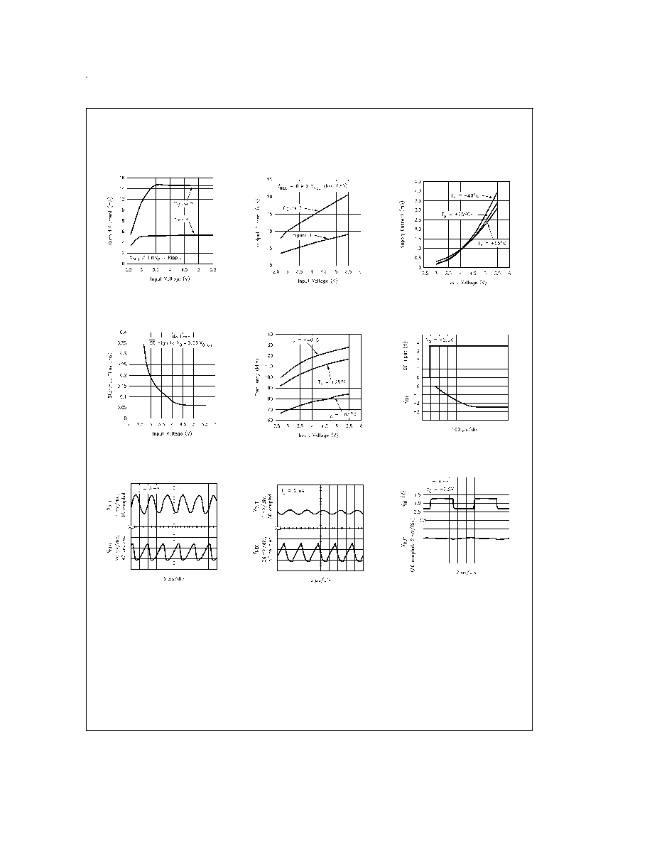
Typical Performance Characteristics
Unless otherwise specified, T
A
= 25∞C, V
OUT
=
-2.5V. (Continued)
Maximum Output Current vs. Input
Voltage
DS101180-7
Maximum V
NEG
Current vs. Input
Voltage
DS101180-8
No Load Supply Current vs. Input
Voltage
DS101180-9
Start-Up Time vs. Input Voltage
Figure 1
DS101180-10
Switching Frequency vs. Input
Voltage
DS101180-11
Start-Up from Shutdown (no load)
Figure 2
DS101180-12
Output Ripple
Figure 1
DS101180-13
Output Ripple
Figure 2
DS101180-14
Line Transient Response
DS101180-17
www.national.com
5
Typical Performance Characteristics
Unless otherwise specified, T
A
= 25∞C, V
OUT
=
-2.5V. (Continued)
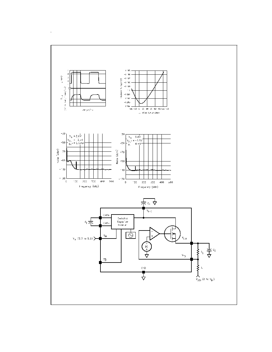
Load Transient Response
DS101180-18
V
FB
vs. Temperature
DS101180-15
Output Noise Spectrum
Figure 1
DS101180-24
Output Noise Spectrum
Figure 2
DS101180-23
DS101180-3
FIGURE 3. Functional Block Diagram
www.national.com
6
Device Description
The LM2687 is an inverting, regulated charge-pump power
converter. It features low noise, small physical size, and is
simple to use. It is an ideal solution for biasing GaAsFET de-
vices such as power amplifier modules found in portable de-
vices and cellular phones.
A switched capacitor charge-pump circuit is used to invert
the input voltage V
IN
to its corresponding negative value
which is seen at V
NEG
. This voltage is regulated by a low
dropout linear regulator at V
OUT
(
Figure 3). The output volt-
age can be regulated anywhere from -1.5V to -5.2V and is
determined by a pair of feedback resistors (see Setting the
Output Voltage). The PSRR of the linear regulator reduces
the output voltage ripple produced by the charge-pump in-
verter to 1mV
P-P
(typical) at the output V
OUT
. The regulator
also attenuates noise from the incoming supply due to its
high PSRR.
Shutdown
The LM2687 features a logic-level shutdown feature. The
function is active-low and will reduce the supply current to
0.05µA (typical) when engaged. When shutdown is active
V
OUT
and V
NEG
are switched to ground.
Application Information
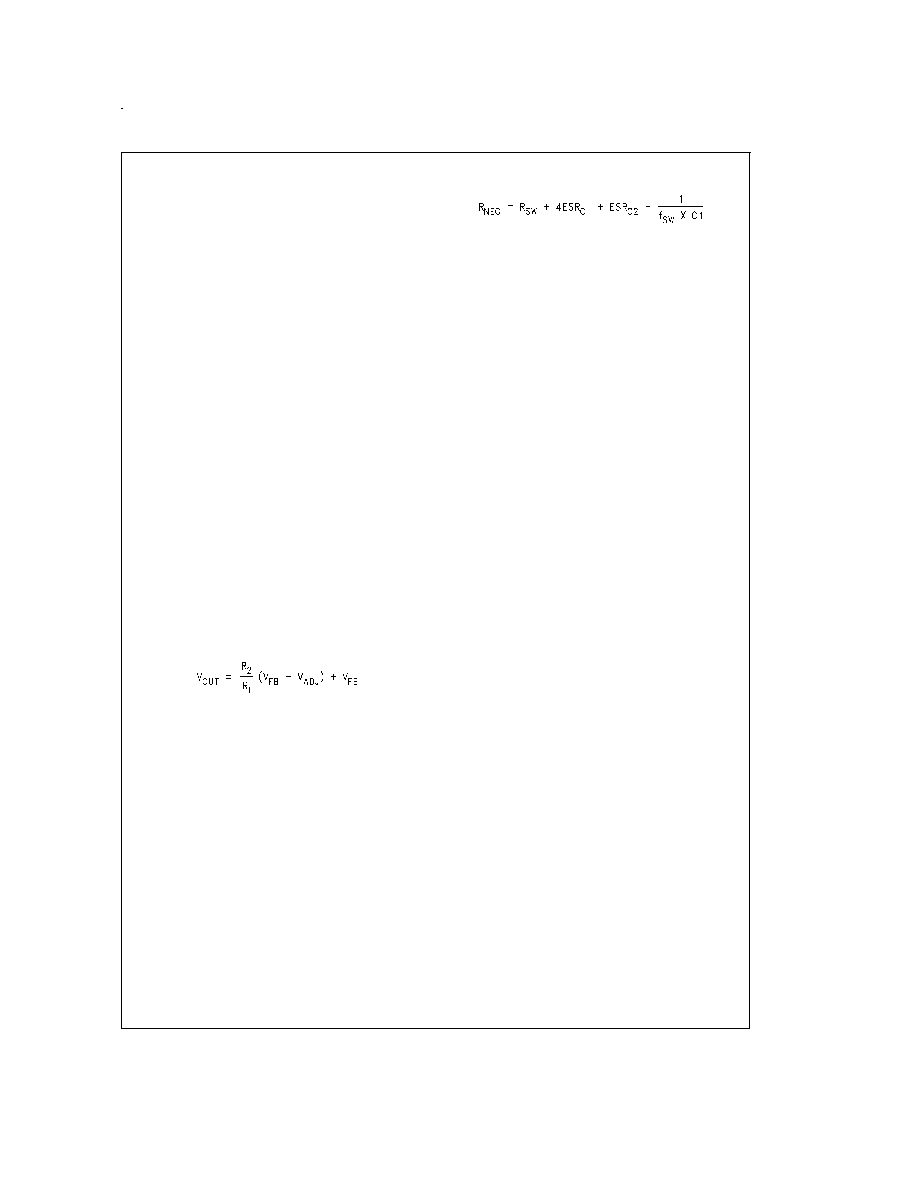
Setting the Output Voltage
The output voltage on the LM2687 is set by using a resistor
divider between the output, the feedback pin, and an arbi-
trary voltage V
ADJ
(
Figure 3). V
ADJ
can range from GND to
any positive voltage up to V
IN
. V
ADJ
is usually chosen to be
GND and should not be connected to a different voltage un-
less it is well regulated so the output will stay constant. The
feedback pin is held at a constant voltage V
FB
which equals
-1.2V. The output voltage can be selected using the equa-
tion:
The current into the feedback pin I
FB
is in the range of 10nA
to 100nA. Therefore using a value of 500k
or smaller for R
1
should make this current of little concern when setting the
output voltage. For best accuracy, use resistors with 1% or
better tolerance.
Capacitor Selection
Selecting the right capacitors for your circuit is important.
The
capacitors
affect
the
output
resistance
of
the
charge-pump, the output voltage ripple, and the overall drop-
out voltage (V
IN
-|V
OUT
|) of the circuit. The output resistance
of the charge-pump inverter is:
The switching frequency is fixed at 100kHz and R
SW
(the
combined resistance of the internal switches) is typically
10
. It is clear from this equation that low ESR capacitors
are desirable and that larger values of C
1
will further reduce
the output resistance. The output resistance of the entire cir-
cuit (in dropout) is:
R
OUT
= R
NEG
+ R
regulator
R
regulator
(the output impedance of the linear regulator) is ap-
proximately 10
. When the circuit is in regulation, the overall
output resistance is equal to the linear regulator load regula-
tion (5mV/mA). The dropout voltage is therefore affected by
the capacitors used since it is simply defined as I
OUT
*
R
OUT
.
A larger value of capacitor and lower ESR for C
2
will lower
the output voltage ripple of the charge-pump. This ripple will
then be subject to the PSRR of the linear regulator and re-
duced at V
OUT
. A larger value and lower ESR for C
3
will fur-
ther reduce this ripple.
The Low Dropout Linear Regulator uses an N-channel FET
device which behaves similarly to an NPN device. Because
of this and the internal compensation there are no strict ESR
requirements for the output capacitor to maintain stability.
Using the minimum recommended values will ensure stabil-
ity under all conditions.
In summation, larger value capacitors with lower ESR will
give the lowest output noise and ripple. C
1
, C
2
, and C
3
should be 1.0µF minimum with less than 0.3
ESR. Larger
values may be used for any or all capacitors. All capacitors
should be either ceramic, surface-mount chip tantalum, or
polymer electrolytic.
Output Noise and Ripple
Low output noise and output voltage ripple are two of the at-
tractive features of the LM2687. Because they are small, the
noise and ripple (1mV typ.) can be hard to measure accu-
rately. Ground loop error between the circuit and the oscillo-
scope caused by the switching of the charge-pump produces
ground currents in the probe wires. This causes sharp volt-
age spikes on the oscilloscope waveform. To reduce this er-
ror measure, the output directly at the output capacitor (C
3
)
and use the shortest wires possible. Also, do not use the
ground lead on the probe. Take the tip cover off of the probe
and touch the grounding ring of the probe directly to the
ground terminal of C
3
. This should give the most accurate
reading of the actual output waveform.
www.national.com
7

Physical Dimensions
inches (millimeters) unless otherwise noted
LIFE SUPPORT POLICY
NATIONAL'S PRODUCTS ARE NOT AUTHORIZED FOR USE AS CRITICAL COMPONENTS IN LIFE SUPPORT
DEVICES OR SYSTEMS WITHOUT THE EXPRESS WRITTEN APPROVAL OF THE PRESIDENT AND GENERAL
COUNSEL OF NATIONAL SEMICONDUCTOR CORPORATION. As used herein:
1. Life support devices or systems are devices or
systems which, (a) are intended for surgical implant
into the body, or (b) support or sustain life, and
whose failure to perform when properly used in
accordance with instructions for use provided in the
labeling, can be reasonably expected to result in a
significant injury to the user.
2. A critical component is any component of a life
support device or system whose failure to perform
can be reasonably expected to cause the failure of
the life support device or system, or to affect its
safety or effectiveness.
National Semiconductor
Corporation
Americas
Tel: 1-800-272-9959
Fax: 1-800-737-7018
Email: support@nsc.com
National Semiconductor
Europe
Fax: +49 (0) 1 80-530 85 86
Email: europe.support@nsc.com
Deutsch Tel: +49 (0) 1 80-530 85 85
English
Tel: +49 (0) 1 80-532 78 32
FranÁais Tel: +49 (0) 1 80-532 93 58
Italiano
Tel: +49 (0) 1 80-534 16 80
National Semiconductor
Asia Pacific Customer
Response Group
Tel: 65-2544466
Fax: 65-2504466
Email: sea.support@nsc.com
National Semiconductor
Japan Ltd.
Tel: 81-3-5639-7560
Fax: 81-3-5639-7507
www.national.com
MSOP-8 Package
8-Lead Mini SO-8 (MM)
For Ordering, Refer to Ordering Information Table
NS Package Number MUA08A
LM2687
Low
Noise
Regulated
Switched
Capacitor
V
oltage
Inverter
National does not assume any responsibility for use of any circuitry described, no circuit patent licenses are implied and National reserves the right at any time without notice to change said circuitry and specifications.