LM2696
3A, Constant On Time Buck Regulator
General Description
The LM2696 is a pulse width modulation (PWM) buck regu-
lator capable of delivering up to 3A into a load. The control
loop utilizes a constant on-time control scheme with input
voltage feed forward. This provides a topology that has
excellent transient response without the need for compen-
sation. The input voltage feed forward ensures that a con-
stant switching frequency is maintained across the entire V
IN
range.
The LM2696 is capable of switching frequencies in the range
of 100 kHz to 500 kHz. Combined with an integrated 130 m
high side NMOS switch the LM2696 can utilize small sized
external components and provide high efficiency. An internal
soft-start and power-good flag are also provided to allow for
simple sequencing between multiple regulators.
The LM2696 is available with an adjustable output in an
exposed pad TSSOP-16 package.
Features
n
Input voltage range of 4.5V�24V
n
Constant On-Time
n
No compensation needed
n
Maximum Load Current of 3A
n
Switching frequency of 100 kHz�500 kHz
n
Constant frequency across input range
n
TTL compatible shutdown thresholds
n
Low standby current of 12 �A
n
130 m
internal MOSFET switch
Applications
n
High efficiency step-down switching regulators
n
LCD Monitors
n
Set-Top Boxes
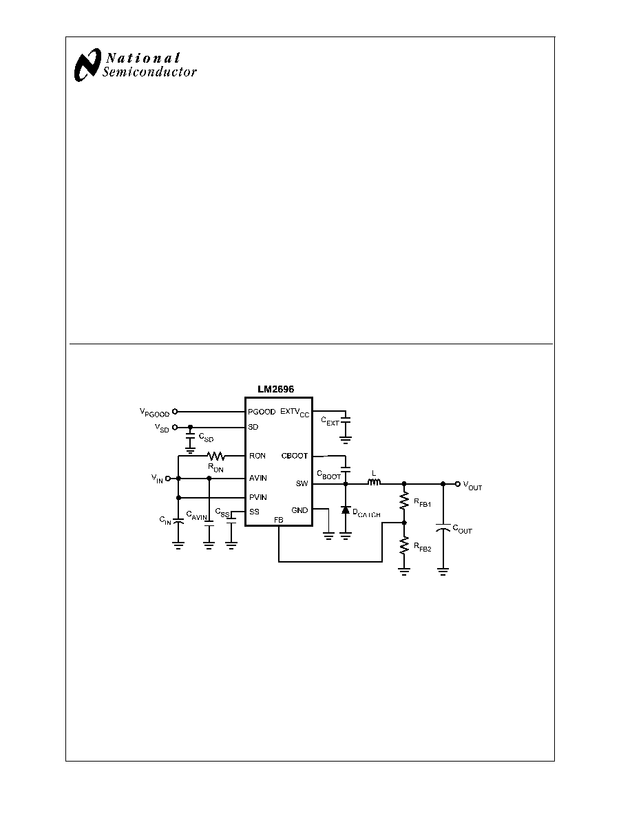
Typical Application Circuit
20153401
October 2005
LM2696
3A,
Constant
On
T
ime
Buck
Regulator
� 2005 National Semiconductor Corporation
DS201534
www.national.com

Connection Diagram
Top View
20153402
eTSSOP-16 Package
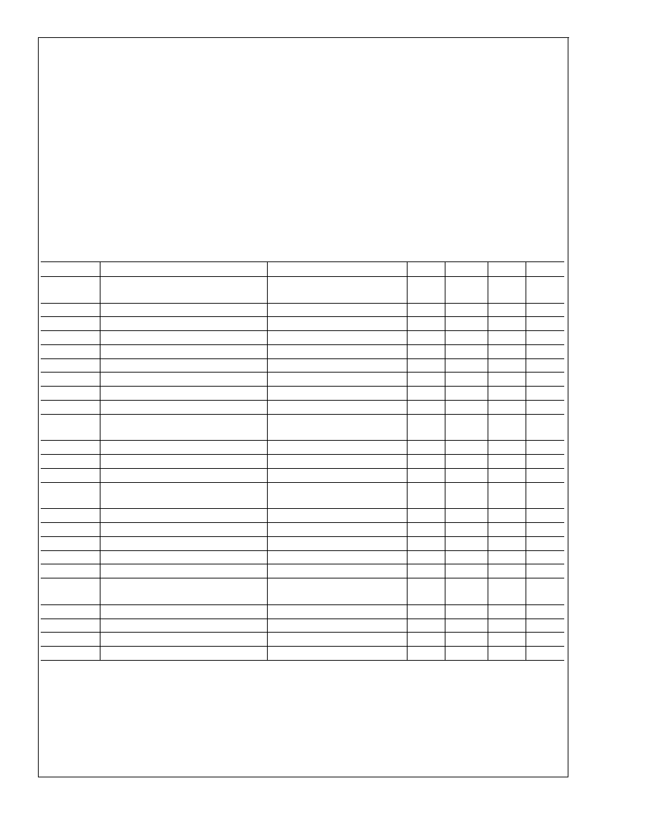
Pin Descriptions
Pin #
Name
Function
1, 2, 3
SW
Switching node
4
CBOOT
Bootstrap capacitor input
5
AVIN
Analog voltage input
6
EXTV
CC
Output of internal regulator for decoupling
7
FB
Feedback signal from output
8
N/C
No connect
9
GND
Ground
10
SS
Soft-start pin
11
PGOOD
Power-good flag, open drain output
12
RON
Sets the switch on-time dependent on current
13
SD
Shutdown pin
14, 15, 16
PVIN
Power voltage input
-
Exposed Pad
Must be connected to ground
Ordering Information
Order
Number
Package
Type
NSC Package
Drawing
Supplied As
LM2696MXA
eTSSOP-16
MXA16A
92 units/rail
LM2696MXAX
eTSSOP-16
MXA16A
2,500 Units Tape and Reel
LM2696
www.national.com
2
Absolute Maximum Ratings
(Note 1)
If Military/Aerospace specified devices are required,
please contact the National Semiconductor Sales Office/
Distributors for availability and specifications.
Voltages from the indicated pins to GND
AVIN
-0.3V to +26V
PVIN
-0.3V to (AV
IN
+0.3V)
CBOOT
-0.3V to +33V
CBOOT to SW
-0.3V to +7V
FB, SD, SS, PGOOD
-0.3V to +7V
Storage Temperature Range
-65�C to +150�C
Junction Temperature
+150�C
Lead Temperature
(Soldering, 10 sec.)
260�C
Minimum ESD Rating
1.5 kV
Operating Range
Junction
Temperature
-40�C to +125�C
AVIN to GND
4.5V to 24V
PVIN
4.5V to 24V
Electrical Characteristics
Specifications with standard typeface are for T
J
= 25�C, and those in boldface
type apply over the full Operating Temperature Range (T
J
= -40�C to +125�C). Minimum and Maximum limits are guaran-
teed through test, design or statistical correlation. Typical values represent the most likely parametric norm at T
J
= 25�C and
are provided for reference purposes only. Unless otherwise specified V
IN
= 12V.
Symbol
Parameter
Condition
Min
Typ
Max
Units
V
FB
Feedback Pin Voltage
V
IN
= 4.5V to 24V
I
SW
= 0A to 3A
1.225
1.254
1.282
V
I
CL
Switch Current Limit
V
CBOOT
= V
SW
+ 5V
3.6
4.9
6.4
A
R
DS_ON
Switch On Resistance
I
SW
= 3A
0.13
0.22
I
Q
Operating Quiescent Current
V
FB
= 1.5V
1.3
2
mA
V
UVLO
AVIN Under Voltage Lockout
Rising V
IN
3.9
4.125
4.3
V
V
UVLO HYS
AVIN Under Voltage Lockout Hysteresis
60
120
mV
I
SD
Shutdown Quiescent Current
V
SD
= 0V
12
25
�A
k
ON
Switch On-Time Constant
I
ON
= 50 �A to 100 �A
50
66
82
�A �s
V
D ON
R
ON
Voltage
0.35
0.65
0.95
V
T
OFF_MIN
Minimum Off Time
FB = 1.24V
FB = 0V
165
12
250
30
ns
�s
T
ON MIN
Minimum On-time
400
ns
V
EXTVCC
EXTV
CC
Voltage
3.30
3.65
4.00
V
V
EXTVCC
EXTV
CC
Load Regulation
I
EXTVCC
= 0 �A to 50 �A
0.03
0.5
%
V
PWRGD
PGOOD Threshold (PGOOD Transition
from Low to High)
With respect to V
FB
91.5
93.5
95.5
%
V
PG_HYS
PGOOD Hysteresis
1
2.1
%
I
OL
PGOOD Low Sink Current
V
PGOOD
= 0.4V
0.5
2
mA
I
OH
PGOOD High Leakage Current
50
nA
I
FB
Feedback Pin Bias Current
V
FB
= 1.2V
0
nA
I
SS_SOURCE
Soft-Start Pin Source Current
V
SS
= 0V
0.7
1
1.4
�A
I
SS SINK
Soft-Start Pin Sink Current
V
SS
= 1.2V
V
SD
= 0V
15
mA
I
SD
Shutdown Pull-Up Current
V
SD
= 0V
1
3
�A
V
IH
SD Pin Minimum High Input Level
1.8
V
V
IL
SD Pin Maximum Low Input Level
0.6
V
J-A
Thermal Resistance
35.1
�C/W
Note 1: Absolute Maximum Ratings indicate limits beyond which damage may occur to the device. Operating Ratings indicate conditions for which the device is
intended to be functional, but do not guarantee specific performance limits. For guaranteed specifications, see Electrical Characteristics.
Note 2: Without PCB copper enhancements. The maximum power dissipation must be derated at elevated temperatures and is limited by T
JMAX
(maximum junction
temperature),
J-A
(junction to ambient thermal resistance) and T
A
(ambient temperature). The maximum power dissipation at any temperature is: P
DissMAX
= (T
JMAX
- T
A
) /
J-A
up to the value listed in the Absolute Maximum Ratings.
J-A
for TSSOP-16 package is 38.1�C/W, T
JMAX
= 125�C.
LM2696
www.national.com
3