LM2698
SIMPLE SWITCHER
ģ
1.35A Boost Regulator
General Description
The LM2698 is a general purpose PWM boost converter.
The 1.9A, 18V, 0.2ohm internal switch enables the LM2698
to provide efficient power conversion to outputs ranging from
2.2V to 17V. It can operate with input voltages as low as 2.2V
and as high as 12V. Current-mode architecture provides
superior line and load regulation and simple frequency com-
pensation over the device's 2.2V to 12V input voltage range.
The LM2698 sets the standard in power density and is
capable of supplying 12V at 400mA from a 5V input. The
LM2698 can also be used in flyback or SEPIC topologies.
The LM2698 SIMPLE SWITCHER
ģ
features a pin selectable
switching frequency of either 600kHz or 1.25MHz. This pro-
motes flexibility in component selection and filtering tech-
niques. A shutdown pin is available to suspend the device
and decrease the quiescent current to 5ĶA. An external
compensation pin gives the user flexibility in setting fre-
quency compensation, which makes possible the use of
small, low ESR ceramic capacitors at the output. Switchers
Made Simple
ģ
software is available to insure a quick, easy
and guaranteed design. The LM2698 is available in a low
profile 8-lead MSOP package.
Features
n
1.9A, 0.2
, internal switch (typical)
n
Operating voltage as low as 2.2V
n
600kHz/1.25MHz adjustable frequency operation
n
Switchers Made Simple
ģ
software
n
8-Lead MSOP package
Applications
n
3.3V to 5V, 5V to 12V conversion
n
Distributed Power
n
Set-Top Boxes
n
DSL Modems
n
Diagnostic Medical Instrumentation
n
Boost Converters
n
Flyback Converters
n
SEPIC Converters
Typical Application Circuit
20012658
SIMPLE SWITCHER
ģ
is a registered trademark of National Semiconductor Corporation.
October 2001
LM2698
SIMPLE
SWITCHER
ģ
1.35A
Boost
Regulator
© 2001 National Semiconductor Corporation
DS200126
www.national.com
Connection Diagram
Top View
20012604
8-Lead Plastic MSOP
NS Package Number MUA08A
Ordering Information
Order Number
Package Type
NSC Package
Drawing
Supplied As
Package ID
LM2698MM-ADJ
MSOP-8
MUA08A
1000 Units, Tape and Reel
S22B
LM2698MMX-ADJ
MSOP-8
MUA08A
3500 Units, Tape and Reel
S22B
Pin Description
Pin
Name
Function
1
V
C
Compensation network connection. Connected to the output of the voltage error amplifier.
2
FB
Output voltage feedback input.
3
SHDN
Shutdown control input, active low.
4
GND
Analog and power ground.
5
V
SW
Power switch input. Switch connected between SW pin and GND pin.
6
V
IN
Analog power input.
7
FSLCT
Switching frequency select input. V
IN
= 1.25MHz. Ground = 600kHz.
8
NC
Connect to ground.
LM2698
www.national.com
2
Block Diagram
20012603
LM2698
www.national.com
3

Absolute Maximum Ratings
(Note 1)
If Military/Aerospace specified devices are required,
please contact the National Semiconductor Sales Office/
Distributors for availability and specifications.
V
IN
-0.3V
V
IN
12V
SW Voltage
-0.3V
V
SW
18V
FB Voltage
-0.3V
V
FB
7V
V
C
Voltage
0.965
<
V
C
<
1.565
SHDN Voltage
(Note 2)
-0.3V
V
SHDN
7V
FSLCT
(Note 2)
-0.3V
V
FSLCT
12V
Maximum Junction
Temperature
150įC
Power Dissipation (Note 3)
Internally Limited
Lead Temperature
300įC
Vapor Phase (60 sec.)
215įC
Infrared (15 sec.)
220įC
ESD Susceptibility
(Note 4)
Human Body Model
(Note 5)
2kV
Machine Model
200V
Operating Conditions
Operating Junction
Temperature Range
(Note 6)
-40įC to +125įC
Storage Temperature
-65įC to +150įC
Supply Voltage
2.2V to 12V
SW Voltage
0
V
SW
17.5V
Electrical Characteristics
Specifications in standard type face are for T
J
= 25įC and those with boldface type apply over the full Operating Tempera-
ture Range ( T
J
= -40įC to +125įC)Unless otherwise specified. V
IN
=2.2V and I
L
= 0A, unless otherwise specified.
Symbol
Parameter
Conditions
Min
(Note 6)
Typ
(Note 7)
Max
(Note 6)
Units
I
Q
Quiescent Current
FB = 0V (Not Switching)
1.3
2.0
mA
V
SHDN
= 0V
5
10
ĶA
V
FB
Feedback Voltage
1.2285
1.26
1.2915
V
I
CL
Switch Current Limit
V
IN
= 2.7V (Note 8)
1.35
1.9
2.4
A
%V
FB
/
V
IN
Feedback Voltage Line
Regulation
2.2V
V
IN
12.0V
0.013
0.1
%/V
I
B
FB Pin Bias Current
(Note 9)
0.5
20
nA
V
IN
Input Voltage Range
2.2
12
V
g
m
Error Amp Transconductance
I = 5ĶA
40
135
290
Ķmho
A
V
Error Amp Voltage Gain
120
V/V
D
MAX
Maximum Duty Cycle
FSLCT = Ground
78
85
%
D
MIN
Minimum Duty Cycle
FSLCT = Ground
15
%
FSLCT = V
IN
30
f
S
Switching Frequency
FSLCT = Ground
480
600
720
kHz
FSLCT = V
IN
1
1.25
1.5
MHz
I
SHDN
Shutdown Pin Current
V
SHDN
= V
IN
0.01
0.1
ĶA
V
SHDN
= 0V
-0.5
-1
I
L
Switch Leakage Current
V
SW
= 18V
0.01
3
ĶA
R
DS(ON)
Switch R
DS(ON)
V
IN
= 2.7V, I
SW
= 1A
0.2
0.4
TH
SHDN
SHDN Threshold Voltage
Output High
0.6
0.9
V
Output Low
0.3
0.6
V
UVP
On Threshold
1.95
2.05
2.2
V
Off Threshold
1.85
1.95
2.1
V
LM2698
www.national.com
4

Electrical Characteristics
(Continued)
Specifications in standard type face are for T
J
= 25įC and those with boldface type apply over the full Operating Tempera-
ture Range ( T
J
= -40įC to +125įC)Unless otherwise specified. V
IN
=2.2V and I
L
= 0A, unless otherwise specified.
Symbol
Parameter
Conditions
Min
(Note 6)
Typ
(Note 7)
Max
(Note 6)
Units
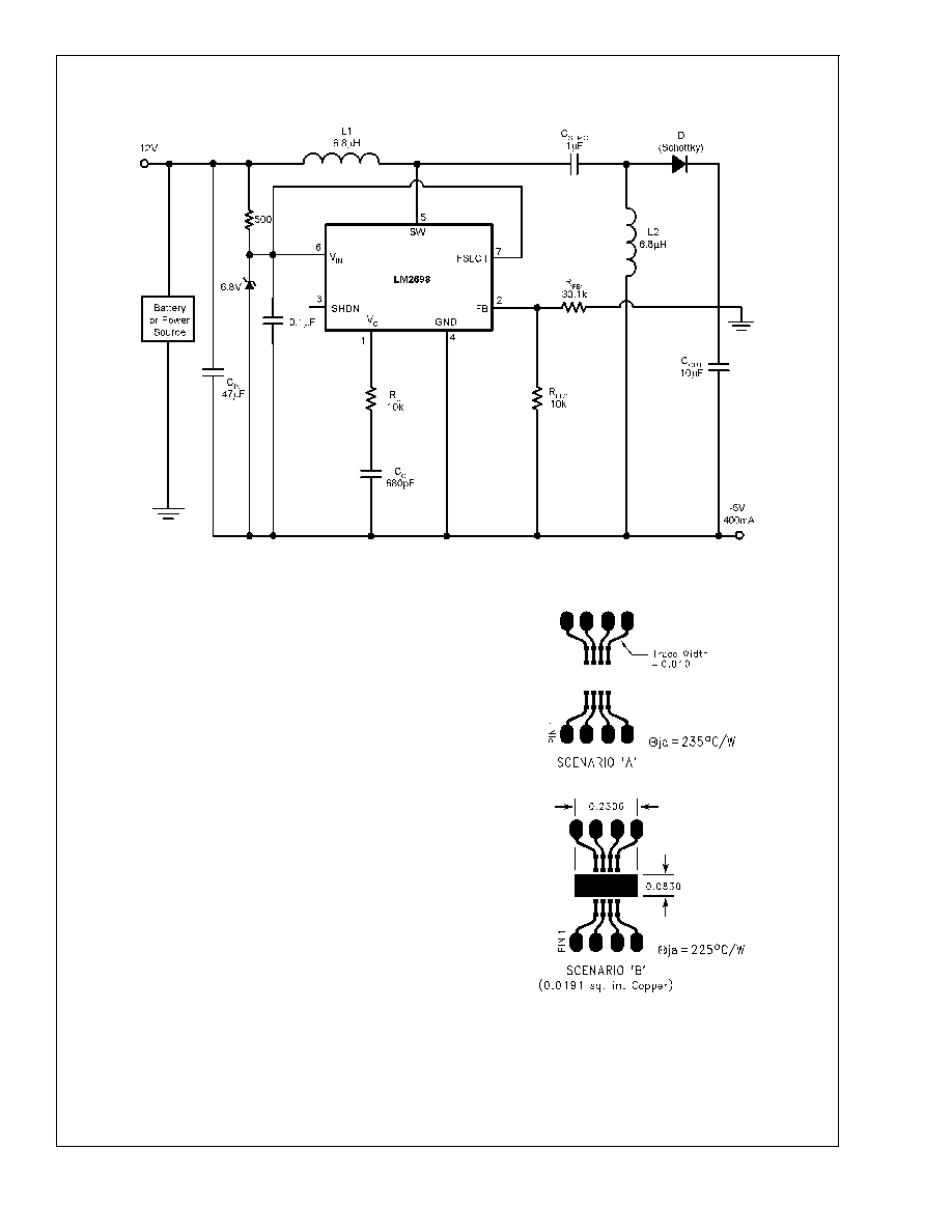
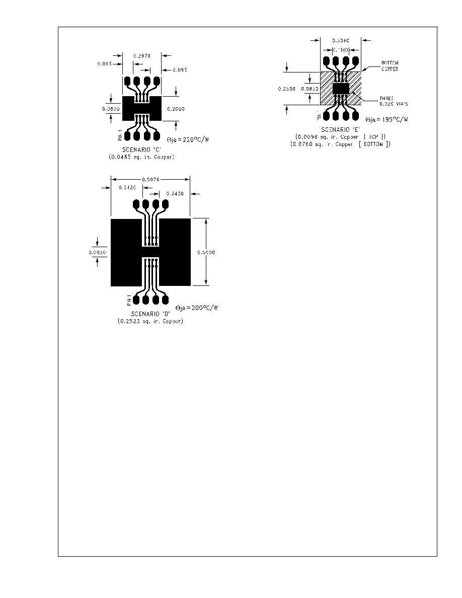
JA
Thermal Resistance
Junction to Ambient
(Note 10)
235
įC/W
Junction to Ambient
(Note 11)
225
Junction to Ambient
(Note 12)
220
Junction to Ambient
(Note 13)
200
Junction to Ambient
(Note 14)
195
Note 1: Absolute maximum ratings are limits beyond which damage to the device may occur. Operating Ratings are conditions for which the device is intended to
be functional, but device parameter specifications may not be guaranteed. For guaranteed specifications and test conditions, see the Electrical Characteristics.
Note 2: Shutdown and voltage frequency select should not exceed V
IN
.
Note 3: The maximum allowable power dissipation is a function of the maximum junction temperature, T
J
(MAX), the junction-to-ambient thermal resistance,
JA
,
and the ambient temperature, T
A
. See the Electrical Characteristics table for the thermal resistance of various layouts. The maximum allowable power dissipation
at any ambient temperature is calculated using: P
D
(MAX) = (T
J(MAX)
- T
A
)/
JA
. Exceeding the maximum allowable power dissipation will cause excessive die
temperature, and the regulator will go into thermal shutdown.
Note 4: The human body model is a 100 pF capacitor discharged through a 1.5k
resistor into each pin. The machine model is a 200pF capacitor discharged
directly into each pin.
Note 5: ESD susceptibility using the human body model is 500V for V
C
.
Note 6: All limits guaranteed at room temperature (standard typeface) and at temperature extremes (bold typeface). All room temperature limits are 100% tested
or guaranteed through statistical analysis. All limits at temperature extremes are guaranteed via correlation using standard Statistical Quality Control (SQC) methods.
All limits are used to calculate Average Outgoing Quality Level (AOQL).
Note 7: Typical numbers are at 25įC and represent the most likely norm.
Note 8: This is the switch current limit at 0% duty cycle. The switch current limit will change as a function of duty cycle. See Typical performance Characteristics
section for I
CL
vs. V
IN
Note 9: Bias current flows into FB pin.
Note 10: Junction to ambient thermal resistance (no external heat sink) for the MSO8 package with minimal trace widths (0.010 inches) from the pins to the circuit.
See 'Scenario 'A'' in the Power Dissipation section.
Note 11: Junction to ambient thermal resistance for the MSO8 package with minimal trace widths (0.010 inches) from the pins to the circuit and approximately
0.0191 sq. in. of copper heat sinking. See 'Scenario 'B'' in the Power Dissipation section.
Note 12: Junction to ambient thermal resistance for the MSO8 package with minimal trace widths (0.010 inches) from the pins to the circuit and approximately
0.0465 sq. in. of copper heat sinking. See 'Scenario 'C'' in the Power Dissipation section.
Note 13: Junction to ambient thermal resistance for the MSO8 package with minimal trace widths (0.010 inches) from the pins to the circuit and approximately
0.2523 sq. in. of copper heat sinking. See 'Scenario 'D'' in the Power Dissipation section.
Note 14: Junction to ambient thermal resistance for the MSO8 package with minimal trace widths (0.010 inches) from the pins to the circuit and approximately
0.0098 sq. in. of copper heat sinking on the top layer and 0.0760 sq. in. of copper heat sinking on the bottom layer, with three 0.020 in. vias connecting the planes.
See 'Scenario 'E'' in the Power Dissipation section.
LM2698
www.national.com
5
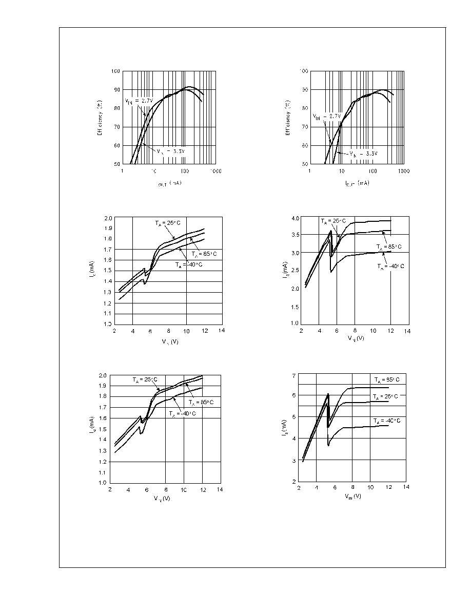
Typical Performance Characteristics
Efficiency vs Load Current
(V
OUT
= 8V, f
S
= 600kHz)
Efficiency vs Load Current
(V
OUT
= 8V, f
S
= 1.25MHz)
20012667
20012666
I
q
vs V
IN
(600 kHz, non-switching)
I
q
vs V
IN
(600 kHz, switching)
20012618
20012619
I
q
vs. V
IN
(1.25MHz, non-switching)
I
q
vs V
IN
(1.25MHz, switching)
20012622
20012617
LM2698
www.national.com
6
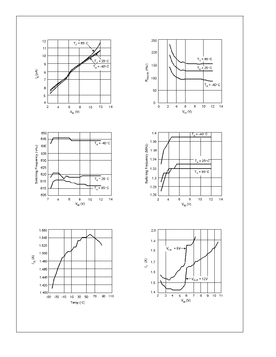
Typical Performance Characteristics
(Continued)
I
q(SHDN)
vs V
IN
R
DS(ON)
vs V
IN
20012616
20012621
Switching Frequency vs V
IN
(600kHz)
Switching Frequency vs V
IN
(1.25MHz)
20012620
20012623
I
CL
vs. Ambient Temperature
V
IN
= 3.3V, V
OUT
= 8V
I
CL
vs. V
IN
20012641
20012642
LM2698
www.national.com
7
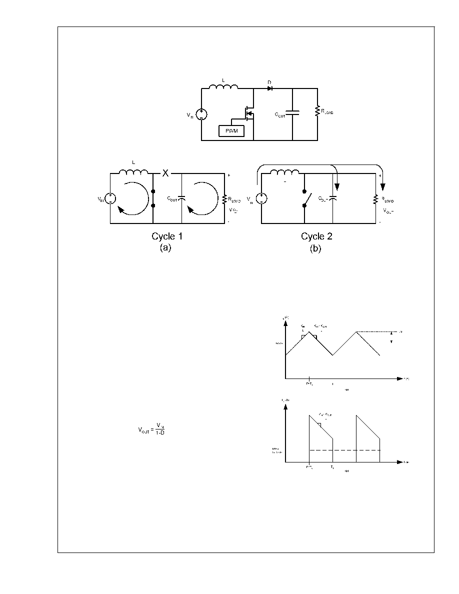
Operation
Continuous Conduction Mode
The LM2698 is a current-mode, PWM boost regulator. A
boost regulator steps the input voltage up to a higher output
voltage. In continuous conduction mode (when the inductor
current never reaches zero at steady state), the boost regu-
lator operates in two cycles.
In the first cycle of operation, shown in
Figure 1 (a), the
transistor is closed and the diode is reverse biased. Energy
is collected in the inductor and the load current is supplied by
C
OUT
.
The second cycle is shown in
Figure 1 (b). During this cycle,
the transistor is open and the diode is forward biased. The
energy stored in the inductor is transferred to the load and
output capacitor.
The ratio of these two cycles determines the output voltage.
The output voltage is defined as:
where D is the duty cycle of the switch.
Inductor
The inductor is one of the two energy storage elements in a
boost converter.
Figure 2 shows how the inductor current
varies during a switching cycle. The current through an
inductor is quantified as:
20012602
FIGURE 1. Simplified Boost Converter Diagram
(a) First Cycle of Operation (b) Second Cycle Of Operation
20012605
FIGURE 2. (a) Inductor Current (b) Diode Current
LM2698
www.national.com
8
Operation
(Continued)
If V
L(t)
is constant, di
L
/ dt must be constant, thus the current
in the inductor changes at a constant rate. This is the case in
DC/DC converters since the voltages at the input and output
can be approximated as a constant. The current through the
inductor of the LM2698 boost converter is shown in
Figure
2(a). The important quantities in determining a proper induc-
tance value are I
L(AVG)
(the average inductor current) and
i
L
(the inductor current ripple). If
i
L
is larger than I
L(AVG)
, the
inductor current will drop to zero for a portion of the cycle and
the converter will operate in discontinuous conduction mode.
If
i
L
is smaller than I
L(AVG)
, the inductor current will stay
above zero and the converter will operate in continuous
conduction mode (CCM). All the analysis in this datasheet
assumes operation in continuous conduction mode. To op-
erate in CCM:
I
L(AVG)
>
i
L
Choose the minimum I
OUT
to determine the minimum L for
CCM operation. A common choice is to set
i
L
to 30% of
I
L(AVG)
.
The inductance value will also affect the stability of the
converter. Because the LM2698 utilizes current mode con-
trol, the inductor value must be carefully chosen. See the
COMPENSATION section for recommended inductance val-
ues.
Choosing an appropriate core size for the inductor involves
calculating the average and peak currents expected through
the inductor. In a boost converter,
and
I
L(Peak)
= I
L(AVG)
+
i
L
,
where
A core size with ratings higher than these values should be
chosen. If the core is not properly rated, saturation will
dramatically reduce overall efficiency.
Current Limit
The current limit in the LM2698 is referenced to the peak
switch current. The peak currents in the switch of a boost
converter will always be higher than the average current
supplied to the load. To determine the maximum average
output current that the LM2698 can supply, use:
I
OUT(MAX)
= (I
CL
-
i
L
)
*
(1-D) = (I
CL
-
i
L
)
*
V
IN
/V
OUT
Where I
CL
is the switch current limit (see Electrical Chara-
teristics table and Typical Performance Curves). Hence, as
V
IN
increases, the maximum current that can be supplied to
the load increases, as shown in
Figure 3.
Diode
The diode in a boost converter such as the LM2698 acts as
a switch to the output. During the first cycle, when the
transistor is closed, the diode is reverse biased and current
is blocked; the load current is supplied by the output capaci-
tor. In the second cycle, the transistor is open and the diode
is forward biased; the load current is supplied by the induc-
tor.
Observation of the boost converter circuit shows that the
average current through the diode is the average load cur-
rent, and the peak current through the diode is the peak
current through the inductor. The diode should be rated to
handle more than its peak current. To improve efficiency, a
low forward drop Schottky diode is recommended.
Input Capacitor
Due to the presence of an inductor at the input of a boost
converter, the input current waveform is continuous and
triangular. The inductor ensures that the input capacitor sees
fairly low ripple currents. However, as the inductor gets
smaller, the input ripple increases. The rms current in the
input capacitor is given by:
The input capacitor should be capable of handling the rms
current. Although the input capacitor is not so critical in boost
applications, a 10 ĶF or higher value, good quality capacitor
prevents any impedance interactions with the input supply.
A 0.1ĶF or 1ĶF ceramic bypass capacitor is also recom-
mended on the V
IN
pin (pin 6) of the IC. This capacitor must
20012673
FIGURE 3. Maximum Output Current vs Input Voltage
LM2698
www.national.com
9

Operation
(Continued)
be connected very close to pin 6 to effectively filter high
frequency noise. When operating at 1.25 MHz switching
frequency, a minimum bypass capacitance of 0.22 ĶF is
recommended.
Output Capacitor
The output capacitor in a boost converter provides all the
output current when the switch is closed and the inductor is
charging. As a result, it sees very large ripple currents. The
output capacitor should be capable of handling the maxi-
mum RMS current. The RMS current in the output capacitor
is:
where,
and
D = (V
OUT
- V
IN
)/V
OUT
The ESR and ESL of the output capacitor directly control the
output ripple. Use capacitors with low ESR and ESL at the
output for high efficiency and low ripple voltage. Surface
mount tantalums, surface mount polymer electrolytic, and
polymer tantalum, Sanyo OS-CON, or multi-layer ceramic
capacitors are recommended at the output.
Compensation
This section presents a step-by-step procedure to design the
compensation network at pin 1 (V
c
) of the LM2698. These
design methods will produce a conservative and stable con-
trol loop.
There is a minimum inductance requirement in any current
mode converter. This is a function of V
OUT
, duty cycle, and
switching frequency, among other things. The graphs below
plot the recommended inductance range vs. duty cycle for
V
OUT
= 12V. The two lines represent the upper and lower
bounds of the recommended inductance range. The simpli-
fied compensation procedure that follows assumes that the
inductance never drops below the Q = 5 line.
Figure 4 plots
the equation:
(1)
where,
R
DSON
= 0.15,
Se = 0.072
*
f
S
,
and Q = 0.5 and 5
Use Q = 5 to calculate the minimum inductance recom-
mended for a stable design. Choosing an inductor between
the Q = 0.5 and Q = 5 values provides a good tradeoff
between size and stability. Note that as V
IN
drops less than
5V, R
DS(ON)
increases, as shown in the Typical Performance
Characteristics section (R
DS(ON)
vs.V
IN
curve). The worst
case R
DS(ON)
should be used when choosing the induc-
tance. To view plots for different Vout, multiply the Y axis by
a factor of V
OUT
/12, or plot
Equation (1) for the respective
output voltage.
20012654
20012653
FIGURE 4. Minimum Inductance Requirements for (a) f
S
= 600kHz and (b) f
S
= 1.25MHz
LM2698
www.national.com
10

Operation
(Continued)
The goal of the compensation network is to provide the best
static and dynamic performance while insuring stability over
line and load variations. The relationship of stability and
performance can be best analyzed by plotting the magnitude
and phase of the open loop frequency response in the form
of a bode plot. A typical bode plot of the LM2698 open loop
frequency response is shown in
Figure 5.
Poles are marked with an 'X', and zeros are marked with a
'O'. The bolded 'O' labeled 'f
RHP
' is a right-half plane zero.
Right half plane zeros act like normal zeros to the magnitude
(+20dB/decade slope influence) and like poles to the phase
(-90į shift). Three curves are shown. The powerstage curve
is the frequency response of the powerstage, which includes
the switch, diode, inductor, output capacitor, and load. The
compensator curve is the frequency response of the com-
pensator, which is the error amp combined with the compen-
sation network. T is the product of the powerstage and the
compensator and is the complete open loop frequency re-
sponse. The power stage response is fixed by line and load
constraints, while the compensator is set by the external
compensation network at pin 1. The compensator can be
designed in a few simple steps as follows.
Quick Compensator Design
Calculate:
where,
where R
OUT
= 875k
Choose C
C1
= 4.7nF
Choose
Where,
20012657
FIGURE 5. Bode plot of the LM2698 Frequency Response using the Typical Application Circuit
LM2698
www.national.com
11

Operation
(Continued)
If the output capacitor is of high ESR (0.1
or higher), it may
be necessary to use C
C2
. A rule of thumb is that if
1/(2
C
OUT
ESR) (Hz) is lower than f
S
/2 (Hz), C
C2
should be
used. Choose C
C2
such that:
(R
C
+ R
OUT
)(C
OUT
ESR) / (R
C
R
OUT
) (F)
where R
OUT
= output impedance of the error amp (875 k
).
Improving Transient Response Time
The above compensator design provides a loop gain with
high phase margin for a large stability margin. The transient
response time of this loop is limited by the lower
mid-frequency gain necessary to achieve a high phase mar-
gin. If it is desired to increase the transient response time,
C
C1
may be decreased. Decreasing C
C1
by 2x, 4x, and 6x
will yield increasingly shorter transient response times, how-
ever the loop phase margin will become progressively lower
as C
C1
is decreased. When optimizing the loop gain for
transient response time, it is recommended to keep the
phase margin above 40į.
LM2698
www.national.com
12
Operation
(Continued)
Additional Comments on the Open Loop Frequency Re-
sponse
The procedure used here to pick the compensation network
will provide a good starting point. In most cases, these
values will be sufficient for a stable design. It is always
recommended to check the design in a real test setup. This
is easy to do with the aid of a dynamic load. Set the high and
low load values to your system requirements and switch
between the two at about 1kHz. View the output voltage with
an oscilloscope using AC coupling, and zoom in enough to
see the waveform react to the load change. Use the follow-
ing table to determine if your design is stable. Remember to
use worst case conditions (V
IN(MIN)
, R
OUT(MIN)
, R
OUT(MAX)
).
Response
Conclusion
What to
Change
Underdamped,
weak attenuation
Nearing instability
Make C
C1
larger
Underdamped,
strong attenuation
Stable
Nothing
Critically damped
Stable
Nothing
Overdamped
Stable
Nothing
Application Information
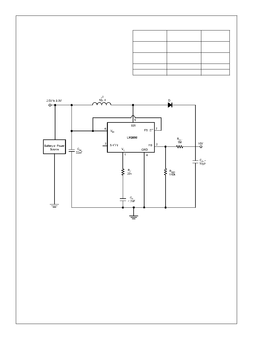
1.25MHz Boost Converter
Figure 6 shows the LM2698 boosting 3.3V to 10V at 300mA.
As discussed in the COMPENSATION section, the R
DS(ON)
of the internal FET in the LM2698 raises as the input voltage
drops below 5V (see Typical Performance Characteristics).
The minimum input voltage for this application is 2.5V, at
which point the R
DS(ON)
is approximately 200m
. Substitut-
ing these values in for
Equation (1), it is found that either a
10 ĶH (1.25MHz operation) or a 22 ĶH (600kHz operation) is
necessary for a stable design. The circuit is operated at
1.25MHz to allow for a smaller inductance. From the Com-
pensator Design equations, R
C
is calculated to be 18.6k
,
and a 20k
resistor is used.
20012668
FIGURE 6. 3.3V to 10V Boost Converter
LM2698
www.national.com
13
Application Information
(Continued)
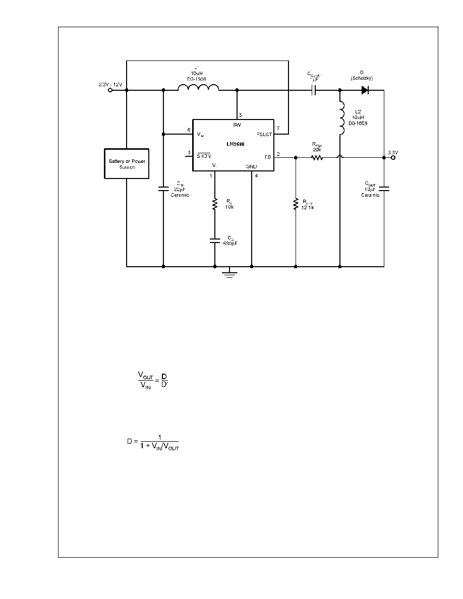
3.3V SEPIC
The LM2698 can be used to implement a SEPIC technology.
The advantages of the SEPIC topology are that it can step
up or step down an input voltage, and it has low input current
ripple.
The conversion ratio for the SEPIC is :
where
D' = 1-D
Solving for D yeilds:
To avoid subharmonic oscillations, it is recommended that
inductors L1 and L2 be the same inductance. Currents con-
ducted by the inductors are:
I
1
= I
OUT
(V
OUT
/V
IN
)
i
1
= V
IN
D/(2
*
L1
*
fs)
I
2
= I
OUT
i
1
= V
IN
D/(2
*
L2
*
fs)
The switch sees a maximum current of I
1
+ I
2
+
i
1
+
i
2
. If
L1 = L2 = L, the maximum switch current is given by:
I
OUT
(1 + V
OUT
/V
IN
) + V
IN
D/(L
*
fs)
The maximum load current is limited by this relationship to
the switch current.
The polarity of C
SEPIC
will change between each cycle, so a
ceramic capacitor should be used here. A high quality, low
ESR capacitor will directly improve efficiency because all the
load current passes through C
SEPIC
.
C
IN
should be chosen using the same relationship as in the
boost converter (see the C
IN
section). C
IN
must be able to
provide the necessary RMS current.
20012631
FIGURE 7. 3.3V SEPIC Converter
LM2698
www.national.com
14
Application Information
(Continued)
Level-Shifted SEPIC
The circuit shown in
Figure 8 is similar to the SEPIC shown
in
Figure 7, except that it is level shifted to provide a negative
output voltage. This is achieved by connecting the ground of
the LM2698 to the output. The circuit analysis for the
level-shifted SEPIC is the same as the SEPIC. The voltage
at the input of the LM2698 will need to be clamped if the
absolute value of the output voltage plus the input voltage
exceeds 12V, the absolute maximum rating for the V
IN
pin.
The simplest way to do this is with a zener diode, as shown
in
Figure 8. Likewise, if the FSLCT pin is pulled high to
operate at 1.25 MHz, its voltage must not exceed 12V. To
prevent any high frequency noise from entering the
LM2698's internal circuitry, a high frequency bypass capaci-
tor must be placed as close to pin 6 as possible. A good
choice for this capacitor is a 0.1ĶF ceramic capacitor.
Power Dissipation
The output power of the LM2698 is limited by its maximum
power dissipation. The maximum power dissipation is deter-
mined by the formula
P
D
= (T
jmax
- T
A
)/
JA
where T
jmax
is the maximum specified junction temperature
(125įC), T
A
is the ambient temperature, and
JA
is the ther-
mal resistance of the package.
JA
is dependant on the
layout of the board as shown below.
20012611
20012612
20012643
FIGURE 8. Level-Shifted SEPIC Converter
LM2698
www.national.com
15
Application Information
(Continued)
20012613
20012614
20012615
LM2698
www.national.com
16

Physical Dimensions
inches (millimeters)
unless otherwise noted
8-Lead Plastic MSOP
NS Package Number MUA08A
LIFE SUPPORT POLICY
NATIONAL'S PRODUCTS ARE NOT AUTHORIZED FOR USE AS CRITICAL COMPONENTS IN LIFE SUPPORT
DEVICES OR SYSTEMS WITHOUT THE EXPRESS WRITTEN APPROVAL OF THE PRESIDENT AND GENERAL
COUNSEL OF NATIONAL SEMICONDUCTOR CORPORATION. As used herein:
1. Life support devices or systems are devices or
systems which, (a) are intended for surgical implant
into the body, or (b) support or sustain life, and
whose failure to perform when properly used in
accordance with instructions for use provided in the
labeling, can be reasonably expected to result in a
significant injury to the user.
2. A critical component is any component of a life
support device or system whose failure to perform
can be reasonably expected to cause the failure of
the life support device or system, or to affect its
safety or effectiveness.
National Semiconductor
Corporation
Americas
Email: support@nsc.com
National Semiconductor
Europe
Fax: +49 (0) 180-530 85 86
Email: europe.support@nsc.com
Deutsch Tel: +49 (0) 69 9508 6208
English
Tel: +44 (0) 870 24 0 2171
FranÁais Tel: +33 (0) 1 41 91 8790
National Semiconductor
Asia Pacific Customer
Response Group
Tel: 65-2544466
Fax: 65-2504466
Email: ap.support@nsc.com
National Semiconductor
Japan Ltd.
Tel: 81-3-5639-7560
Fax: 81-3-5639-7507
www.national.com
LM2698
SIMPLE
SWITCHER
ģ
1.35A
Boost
Regulator
National does not assume any responsibility for use of any circuitry described, no circuit patent licenses are implied and National reserves the right at any time without notice to change said circuitry and specifications.