 | –≠–ª–µ–∫—Ç—Ä–æ–Ω–Ω—ã–π –∫–æ–º–ø–æ–Ω–µ–Ω—Ç: LM2706TLX | –°–∫–∞—á–∞—Ç—å:  PDF PDF  ZIP ZIP |

LM2706
Miniature, Variable, Step-Down DC-DC Converter with
Bypass for RF Power Amplifiers
General Description
The LM2706 DC-DC converter is optimized for powering RF
power amplifiers (PAs) from a single Lithium-Ion cell. It may
also be used in many other applications. It steps down an
input voltage from 2.7V to 5.5V to a variable output from
1.5V to 3.25V up to 300 mA. Output voltage is set using a
V
CON
analog input for controlling power levels and efficiency
of the RF PA. An internal bypass switch allows direct con-
nection to the battery for maximum power to the RF PA.
The device offers 4 modes for mobile phones and similar RF
PA applications. Fixed-frequency PWM mode minimizes RF
interference. Forced Bypass mode turns on an internal by-
pass switch to power the PA directly from the battery. Auto-
matic bypass mode minimizes dropout by turning on the
bypass switch when the battery decays to near the output
voltage. Shutdown mode turns the device off and reduces
battery consumption to 0.1 µA (typ.).
The device also offers internal synchronous rectification for
high efficiency (95% typ at 3.25 V
OUT
, 200 mA, 3.9 V
IN
).
Current limit and thermal overload protection protects the
device and system during fault conditions.
The LM2706 is available in a 10-pin lead free micro SMD
package. This packaging uses National's chip-scale micro
SMD technology and offers the smallest possible size. A high
switching frequency (600 kHz) allows use of tiny surface-
mount components. Only three small external surface-mount
components, an inductor and two ceramic capacitors, are
required.
Key Specifications
n
Operates from a single LiION cell (2.7V to 5.5V)
n
Variable output voltage (1.5V to 3.25V)
n
±
2% DC output voltage precision
n
Internal 105 m
(typ) bypass switch
n
300 mA maximum load capability
n
1.4 mA typ quiescent current
n
0.1 µA typ shutdown current
n
600 kHz PWM switching frequency
n
High efficiency (95% typ at 3.9 V
IN
, 3.25 V
OUT
at
200 mA) from internal synchronous rectification
Features
n
Forced and Automatic Bypass modes
n
Miniature 10-pin lead free micro SMD package
n
Only three tiny surface-mount external components
required
n
Uses small ceramic capacitors
n
Low output voltage ripple (
<
10 mV typ)
n
Internal soft start
n
Current overload protection
n
No external compensation
Applications
n
Mobile Phones
n
Hand-Held Radios
n
RF PC Cards
n
Battery Powered RF Devices
Typical Application Circuit
20040901
PRELIMINARY
February 2004
LM2706
Miniature,
V
ariable,
Step-Down
DC-DC
Converter
with
Bypass
for
RF
Power
Amplifiers
© 2004 National Semiconductor Corporation
DS200409
www.national.com
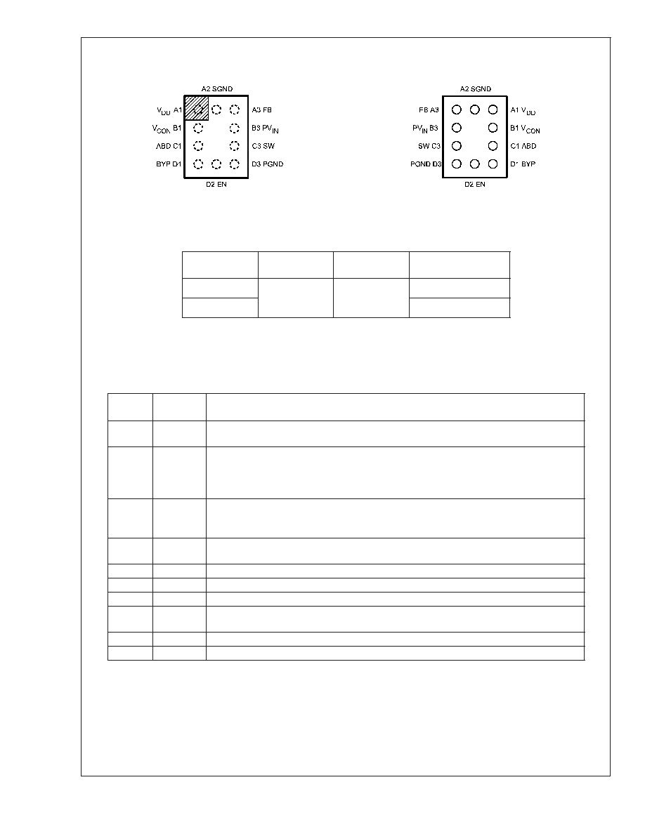
Connection Diagrams
10-Bump micro SMD Package
10-Bump micro SMD Package
20040902
Top View
20040903
Bottom View
Ordering Information
Order Number
Package Type
NSC Package
Marking (*)
Supplied As
LM2706TL
10-Bump Wafer
Level Chip Scale
(micro SMD)
XYTT IS64B
250 Tape and Reel
LM2706TLX
3000 Tape and Reel
(*) XY - denotes the date code marking (2 digit) in production
TT - refers to die run/lot traceability for production
I - pin one indication
S - Product line designator
Note the Package Marking may change over the course of production without notice
Pin Description
Pin
Number
Pin Name
Function
A1
V
DD
Analog Supply Input. If board layout is not optimum, an optional 0.1 µF ceramic capacitor is
suggested (Figure 1).
B1
V
CON
Voltage Control Analog Input. V
CON
controls V
OUT
in PWM mode. Set:
V
CON
0.55V for V
OUT
= 1.5V
0.65V
<
V
CON
<
1.5V for V
OUT
= 1.75 V
CON
+ 0.45V
V
CON
1.7V for V
OUT
= 3.25V
C1
ABD
Automatic Bypass Disable. Use this digital input to control Automatic Bypass mode. Set:
ABD = low to enable automatic bypass mode
ABD = high to disable automatic bypass mode
D1
BYP
Bypass. Use this digital input to command operation in Forced Bypass mode. Set BYP = 0V
for normal operation.
D2
EN
Enable Input. Set this digital input high for normal operation. For shutdown, set low.
D3
PGND
Power Ground
C3
SW
Switching Node connection to the internal PFET switch and NFET synchronous rectifier.
B3
PV
IN
Power Supply Voltage Input to the internal PFET switch. Connect to the input filter capacitor
(Figure 1).
A3
FB
Feedback Analog Input. Connect to the output at the output filter capacitor (Figure 1).
A2
SGND
Analog and Control Ground
LM2706
www.national.com
2

Absolute Maximum Ratings
(Note 1)
If Military/Aerospace specified devices are required,
please contact the National Semiconductor Sales Office/
Distributors for availability and specifications.
Supply Voltage, PV
IN
, V
DD
to SGND
-0.2V to +6V
PGND to SGND
-0.2V to +0.2V
EN, FB, BYP, ABD, V
CON
(SGND -0.2V) to
(V
DD
+0.2V)
SW
(PGND -0.2V) to
(V
DD
+0.2V)
PV
IN
to V
DD
-0.2V to +0.2V
Storage Temperature Range
-45∞C to +150∞C
Lead Temp. (Soldering, 10 sec)
260∞C
Junction Temperature (Note 2)
+125∞C
Minimum ESD Rating
±
2 kV
(Human Body Model, C = 100 pF, R = 1.5 k
)
Thermal Resistance (
JA
) (Note 3)
137∞C/W
Electrical Characteristics
Specifications with standard typeface are for T
A
= T
J
= 25∞C, and those in boldface type apply over the full Operating Tem-
perature Range of T
A
= T
J
= -25∞C to +85∞C. Unless otherwise specified, PV
IN
= V
DD
= EN = 3.6V, BYP = ABD = V
CON
= 0V.
Symbol
Parameter
Conditions
Min
Typ
Max
Units
V
IN
Input Voltage Range (Note 4)
PV
IN
= V
DD
= V
IN
2.7
3.6
5.5
V
V
FB, MIN
Regulated feedback voltage at
minimum setting
V
CON
= 0V
T
A
= 25∞C
1.47
1.50
1.53
V
V
FB, MIN
Regulated feedback voltage at
minimum setting
V
CON
= 0V
1.455
1.50
1.545
V
V
FB, MAX
Regulated feedback voltage at
maximum setting
V
CON
= 1.70V
T
A
= 25∞C
3.185
3.25
3.315
V
V
FB, MAX
Regulated feedback voltage at
maximum setting
V
CON
= 1.70V
3.15
3.25
3.35
V
OVP
Over-Voltage protection Threshold
V
CON
= 0V (Note 5)
260
350
445
mV
V
BYPASS-
Auto Bypass Detection Threshold
V
CON
= 1.7V (Note 6)
160
275
390
mV
V
BYPASS+
Auto Bypass Detection Threshold
V
CON
= 1.7V (Note 6)
310
440
570
mV
I
SHDN
Shutdown Supply Current
EN = ABD = BYP = SW = FB = 0V
T
A
= 25∞C (Note 7)
0.1
1
µA
I
SHDN
Shutdown Supply Current
EN = ABD = BYP = SW = FB = 0V
T
A
= 55∞C (Note 7)
0.45
2
µA
I
SHDN
Shutdown Supply Current
EN = ABD = BYP = SW = FB = 0V
T
A
= 85∞C (Note 7)
6
25
µA
I
Q1_PWM
DC Bias Current into V
DD
FB = 2V, No-Load, V
CON
= 0V
1.4
1.8
mA
I
Q2_BYPASS
V
IN
= BYP = 3.6V,
No-Load, V
CON
= 0V
1.45
1.8
R
DSON(P)
Pin-Pin Resistance for P FET
260
500
m
R
DSON(N)
Pin-Pin Resistance for N FET
200
500
m
R
DSON(BYP)
Pin-Pin Resistance for Bypass
FET
105
200
m
I
LIM, PFET
Switch Peak Current Limit
(Note 8)
550
650
750
mA
I
LIM, BYPASS
Bypass FET Peak Current Limit
(Note 8)
480
650
930
mA
F
OSC
Internal Oscillator Frequency
500
600
700
kHz
V
IH
Logic High Input, EN, BYP, ABD
1.2
V
V
IL
Logic Low Input, EN, BYP, ABD
0.5
V
I
PIN
Pin Pull Down Current, EN, BYP,
ABD
EN, BYP, ABD = 3.6V
5
10
µA
V
CON,MIN
V
CON
Threshold Commanding
V
FB,MIN
PWM Mode, V
CON
Swept Down
0.55
0.6
0.65
V
V
CON,MAX
V
CON
Threshold Commanding
V
FB,MAX
PWM Mode, V
CON
Swept Up
1.5
1.6
1.7
V
Z
CON
V
CON
Input Resistance
100
k
LM2706
www.national.com
3
Electrical Characteristics
(Continued)
Note 1: Absolute Maximum Ratings indicate limits beyond which damage to the device may occur. Operating Ratings indicate conditions for which the device is
functional, but device specifications may not be guaranteed. For guaranteed specifications and associated test conditions, see the Min and Max limits and Conditions
in the Electrical Characteristics table. Electrical characteristics table limits are guaranteed by production testing, design or correlation using standard Statistical
Quality Control methods. Typical (typ) specifications are mean or average values at 25∞C and are not guaranteed.
Note 2: Thermal shutdown will occur if the junction temperature exceeds 150∞C.
Note 3: Thermal resistance specified with 1.2" x 1.2" (2 layer 1.5 oz. Cu.) board.
Note 4: The LM2706 is designed for mobile phone applications where turn-on after power-up is controlled by the system controller and where requirements for a
small package size overrule increased die size for internal Under Voltage Lock-Out (UVLO) circuitry. Thus, it should be kept in shutdown by holding the EN pin low
until the input voltage exceeds 2.7V.
Note 5: Over-Voltage protection (OVP) hysteresis is the voltage above the nominal V
OUT
where the OVP comparator turns off the PFET switch while in PWM mode.
Note 6: V
IN
is compared to the programmed output voltage (V
OUT
, PROG). When V
IN
≠V
OUT
, PROG falls below V
BYPASS-
for longer than T
BYPASS
the bypass FET
turns on and the switching FETS turn off. This is called the bypass mode. Bypass mode is exited when V
IN
≠V
OUT
, PROG exceeds V
BYPASS
+ for longer than
T
BYPASS
, and PWM mode returns.
Note 7: Shutdown current includes the leakage currents of the PFET and Bypass FET.
Note 8: Current limit is built-in, fixed, and not adjustable. The current limit tests are done by using DC measurement methods.
System Characteristics
The following specifications are based on design limits and assume that the compo-
nent values in the typical application circuit are used.These parameters are not guaranteed by production testing.
Symbol
Parameter
Conditions
Min
Typ
Max
Units
Tresponse
Time for V
OUT
to rise from 1.5V to
3.25V (PWM Mode)
V
IN
= 4.2V,C
OUT
= 4.7 µF,
R
LOAD
= 15
25
30
µs
Ton_pwm
Turn on time in pwm mode
EN = L to H,
V
IN
=3.6V,V
OUT
=3.25V,
C
OUT
= 4.7 µF, R
LOAD
=10
600
900
µs
Z
CON
V
CON
input capacitance
V
CON
=1V, Test freq = 100kHz
15
pF
T_bypass
Auto bypass detect delay
(Note 6)
8
10
12
µs
Ton_bypass Bypass FET turn on time
V
IN
- V
OUT
= 0.25V
C
OUT
= 4.7µF, R
LOAD
= 15
30
µs
LM2706
www.national.com
4

Typical Performance Characteristics
(Circuit of Figure 1, V
IN
= EN = 3.6V, ABD = BYP = 0V, T
A
=
25∞C, unless otherwise noted.)
Quiescent Supply Current vs Temperature
Quiescent Supply Current vs Supply Voltage
20040984
20040985
Shutdown Supply Current vs Temperature
Switching Frequency vs Temperature
20040986
20040987
Output Voltage vs Temperature
(V
OUT
= 1.5V)
Output Voltage vs Temperature
(V
OUT
= 3.25V)
20040988
20040989
LM2706
www.national.com
5