LM2717
Dual Step-down DC/DC Converter
General Description
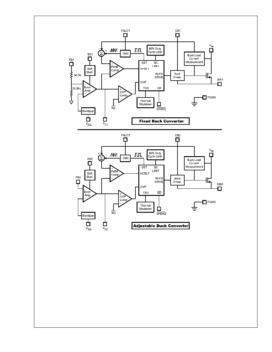
The LM2717 is composed of two PWM DC/DC buck (step-
down) converters. The first converter is used to generate a
fixed output voltage of 3.3V. The second converter is used to
generate an adjustable output voltage. Both converters fea-
ture low R
DSON
(0.16
) internal switches for maximum effi-
ciency. Operating frequency can be adjusted anywhere be-
tween 300kHz and 600kHz allowing the use of small external
components. External soft-start pins for each enables the
user to tailor the soft-start times to a specific application.
Each converter may also be shut down independently with
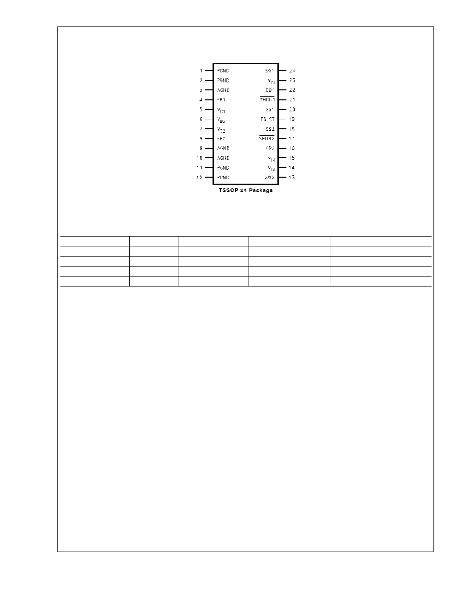
its own shutdown pin. The LM2717 is available in a low
profile 24-lead TSSOP package ensuring a low profile over-
all solution.
Features
n
Fixed 3.3V output buck converter with a 2.2A, 0.16
,
internal switch
n
Adjustable buck converter with a 3.2A, 0.16
, internal
switch
n
Operating input voltage range of 4V to 20V
n
Input undervoltage protection
n
300kHz to 600kHz pin adjustable operating frequency
n
Over temperature protection
n
Small 24-Lead TSSOP package
Applications
n
TFT-LCD Displays
n
Handheld Devices
n
Portable Applications
n
Laptop Computers
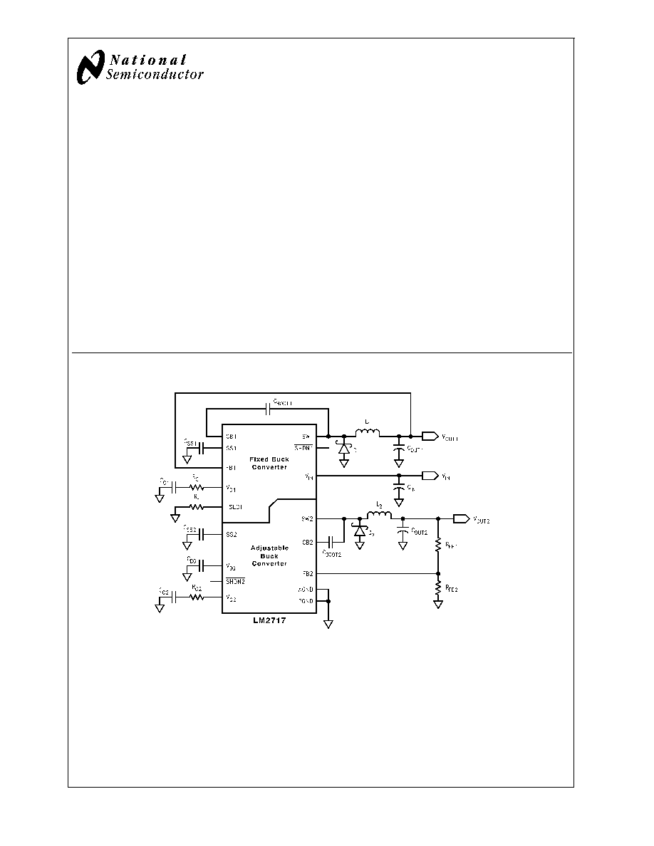
Typical Application Circuit
20078501
PRELIMINARY
May 2005
LM2717
Dual
Step-down
DC/DC
Converter
© 2005 National Semiconductor Corporation
DS200785
www.national.com
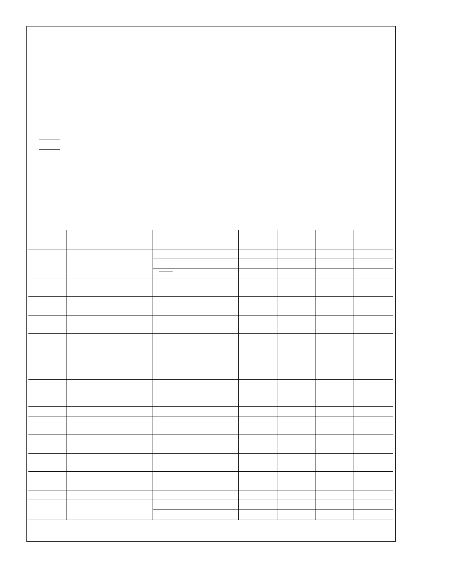
Pin Description
Pin
Name
Function
1
PGND
Power ground. PGND and AGND pins must be connected together directly at the part.
2
PGND
Power ground. PGND and AGND pins must be connected together directly at the part.
3
AGND
Analog ground. PGND and AGND pins must be connected together directly at the part.
4
FB1
Fixed buck output voltage feedback input.
5
V
C1
Fixed buck compensation network connection. Connected to the output of the voltage
error amplifier.
6
V
BG
Bandgap connection.
7
V
C2
Adjustable buck compensation network connection. Connected to the output of the voltage
error amplifier.
8
FB2
Adjustable buck output voltage feedback input.
9
AGND
Analog ground. PGND and AGND pins must be connected together directly at the part.
10
AGND
Analog ground. PGND and AGND pins must be connected together directly at the part.
11
PGND
Power ground. PGND and AGND pins must be connected together directly at the part.
12
PGND
Power ground. PGND and AGND pins must be connected together directly at the part.
13
SW2
Adjustable buck power switch input. Switch connected between V
IN
pins and SW2 pin.
14
V
IN
Analog power input. V
IN
pins should be connected together directly at the part.
15
V
IN
Analog power input. V
IN
pins should be connected together directly at the part.
16
CB2
Adjustable buck converter bootstrap capacitor connection.
17
SHDN2
Shutdown pin for adjustable buck converter. Active low.
18
SS2
Adjustable buck soft start pin.
19
FSLCT
Switching frequency select input. Use a resistor to set the frequency anywhere between
300kHz and 600kHz.
20
SS1
Fixed buck soft start pin.
21
SHDN1
Shutdown pin for fixed buck converter. Active low.
22
CB1
Fixed buck converter bootstrap capacitor connection.
23
V
IN
Analog power input. V
IN
pins should be connected together directly at the part.
24
SW1
Fixed buck power switch input. Switch connected between V
IN
pins and SW1 pin.
LM2717
www.national.com
3
Absolute Maximum Ratings
(Note 1)
If Military/Aerospace specified devices are required,
please contact the National Semiconductor Sales Office/
Distributors for availability and specifications.
V
IN
-0.3V to 22V
SW1 Voltage
-0.3V to 22V
SW2 Voltage
-0.3V to 22V
FB1 Voltage
-0.3V to 7V
FB2 Voltage
-0.3V to 7V
V
C1
Voltage
1.75V
V
C1
2.25V
V
C2
Voltage
0.965V
V
C2
1.565V
SHDN1 Voltage
-0.3V to 7.5V
SHDN2 Voltage
-0.3V to 7.5V
SS1 Voltage
-0.3V to 2.1V
SS2 Voltage
-0.3V to 2.1V
FSLCT Voltage
AGND to 5V
Maximum Junction Temperature
150∞C
Power Dissipation(Note 2)
Internally Limited
Lead Temperature
300∞C
Vapor Phase (60 sec.)
215∞C
Infrared (15 sec.)
220∞C
ESD Susceptibility (Note 3)
Human Body Model
2kV
Operating Conditions
Operating Junction
Temperature Range
(Note 4)
-40∞C to +125∞C
Storage Temperature
-65∞C to +150∞C
Supply Voltage
4V to 20V
SW1 Voltage
20V
SW2 Voltage
20V
Electrical Characteristics
Specifications in standard type face are for T
J
= 25∞C and those with boldface type apply over the full Operating Tempera-
ture Range (T
J
= -40∞C to +125∞C). V
IN
= 5V, I
L
= 0A, and F
SW
= 300kHz unless otherwise specified.
Symbol
Parameter
Conditions
Min
(Note 4)
Typ
(Note 5)
Max
(Note 4)
Units
I
Q
Total Quiescent Current (both
switchers)
Not Switching
2.7
6
mA
Switching, switch open
6
12
mA
V
SHDN
= 0V
9
27
µA
V
FB1
Fixed Buck Feedback
Voltage
3.3
V
V
FB2
Adjustable Buck Feedback
Voltage
1.267
V
I
CL1
(Note 6) Fixed Buck Switch Current
Limit
V
IN
= 8V (Note 7)
2.2
A
I
CL2
(Note 6) Adjustable Buck Switch
Current Limit
V
IN
= 8V (Note 7)
3.2
A
I
B1
Fixed Buck FB Pin Bias
Current
(Note 8)
V
IN
= 20V
65
µA
I
B2
Adjustable Buck FB Pin Bias
Current
(Note 8)
V
IN
= 20V
65
nA
V
IN
Input Voltage Range
4
20
V
g
m1
Fixed Buck Error Amp
Transconductance
I = 20µA
1340
µmho
g
m2
Adjustable Buck Error Amp
Transconductance
I = 20µA
1360
µmho
A
V1
Fixed Buck Error Amp
Voltage Gain
134
V/V
A
V2
Adjustable Buck Error Amp
Voltage Gain
136
V/V
D
MAX
Maximum Duty Cycle
89
93
%
F
SW
Switching Frequency
R
F
= 46.4k
200
300
400
kHz
R
F
= 22.6k
475
600
775
kHz
LM2717
www.national.com
5