LM27213
Single Phase Hysteretic Buck Controller
General Description
The LM27213 is a single-phase synchronous buck regulator
controller designed to fully support a portable microproces-
sor. On-chip gate drive makes for a compact, single chip
solution. Output currents in excess of 25 Amps are possible.
The IC employs a current mode hysteretic control mecha-
nism. Inductor current is sensed through a low value sense
resistor.
The LM27213 will operate over an input voltage range of 5V
to 30V. The output voltage is programmed through 6 Voltage
Identification (VID) pins and ranges from 0.700V to 1.708V in
64 steps.
Since the error in the output voltage directly sets the inductor
current, the dynamic response to a large, fast load transient
is close to a square wave. This is optimal for mode transition
requirements. Also, due to the intrinsic input voltage feedfor-
ward characteristic of hysteretic control, the line transient
response is excellent as well.
The IC provides cycle-by-cycle peak current limit, over-
voltage protection, and a power good signal. The LM27213
fully supports the Stop CPU and Sleep modes offered by
some processors. When enabled, the IC enters a power-
saving "diode emulator" mode which helps prolong battery
runtime for portable systems.
The LM27213 also has a soft start feature for the external
adjustment of soft start speed.
Features
n
Ideal load and line transient responses
n
5V to 30V input range
n
On-chip gate drive
n
Convenient CLK_EN# signal
n
Input under-voltage lockout
n
High light-load efficiency
n
Adjustable analog soft start
n
Peak current limit
n
Over-voltage protection
n
Error correction for good static accuracy
n
±
1% DAC accurcy over temperature
n
Interfaces with the LM2647 system supply
n
Available in TSSOP or tiny LLP package
Applications
n
Core voltage supply for Low Power Processors
n
Low voltage high current buck regulators
Benefits
n
Single chip core power solution
n
Minimum output capacitance required
n
Low cost, compact design
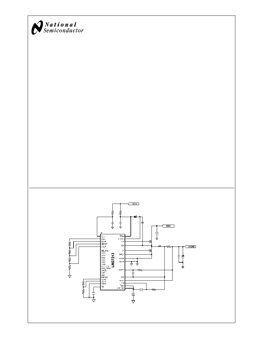
Typical Application
20154330
February 2006
LM27213
Single
Phase
Hysteretic
Buck
Controller
© 2006 National Semiconductor Corporation
DS201543
www.national.com

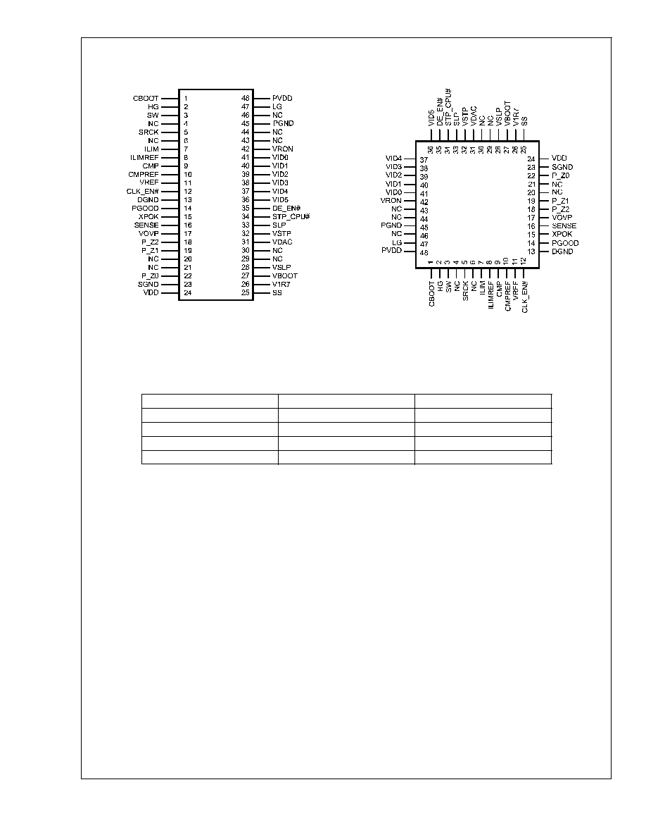
Pin Descriptions (TSSOP/LLP)
Pin 1, CBOOT: Connection for the high-side drive bootstrap
capacitor.
Pin 2, HG: High-side FET gate drive output.
Pin 3, SW: Connect to switch node (drain of bottom power
FET) to detect inductor current reversal. Also serves as the
return path for the high-side FET gate drive currents.
Pin 4, NC:No connect.
Pin 5, SRCK: Source Kelvin. Connect directly to source of
low-side FET to detect negative inductor current.
Pin 6, NC: No connect
Pin 7, ILIM: Over-current sense. Voltage between this pin
and the regulator output is the voltage across the current
sense resistor.
Pin 8, ILIMREF: Current limit reference. Voltage between
this pin and the regulator output sets the inductor current
limit level.
Pin 9, CMP: Current sense. Voltage between this pin and
the regulator output sets the cycle by cycle inductor current.
Pin 10, CMPREF: Inductor current reference. Voltage be-
tween this pin and the regulator output programs the induc-
tor current.
Pin 11, VREF: Desired regulator output voltage under no
load.
Pin 12, CLK_EN#: Signal to start clock chip PLL locking. A
low level indicates that the core supply is now stable and the
CPU can begin clocking.
Pin 13, DGND: Digital ground.
Pin 14, PGOOD: Power good flag. Open-drain output. Logic
high when output voltage enters the power good window and
XPOK is asserted. Masked during transitions.
Pin 15, XPOK: Input that tells the LM27213 that the supply
voltage for the Memory Controller Hub is up. The LM27213
will regulate the output voltage to VBOOT until XPOK tran-
sitions to a high state. PGOOD is forced low as long as this
pin is low.
Pin 16, SENSE: Regulator output voltage sense. Connect
directly to output.
Pin 17, VOVP: Over-voltage protection level. Connect this
pin to the desired reference voltage to set the trigger level for
over-voltage protection.
Pins 18 P_Z2: Factory reference trim, do not connect. This
pin must float.
Pin 19, P_Z1: Factory reference trim, do not connect. This
pin must float.
Pins 20 NC: No connect.
Pin 21, NC: No connect
Pin 22, P_Z0: Factory reference trim, do not connect. This
pin must float.
Pin 23, SGND: Signal Ground.
Pin 24, VDD: Chip power supply.
Pin 25, SS: : Soft start, soft shutdown and slew rate control.
Connect a capacitor between this pin and ground to control
the soft start and soft shutdown speed. The value of the
capacitor will also define the slew rate of the dynamic VID
transitions.
Pin 26, VIR7: 1.7V reference voltage.
Pin 27, VBOOT: Initial output voltage desired after soft start
completes. Connect this pin to the desired reference level.
Pin 28, VSLP: Desired Voltage in Sleep Mode. Connect this
pin to the desired reference level.
Pin 29, NC: : No connect.
Pin 30, NC: No connect.
Pin 31, VDAC: Buffered Digital-to-Analog converter output.
Pins 32, VSTP: Desired output voltage in Stop CPU mode.
Connect this pin to the desired reference level.
Pin 33, SLP: When this pin is logic high, VREF voltage is
equal to that on the VSLP pin.
Pin 34, STP_CPU#: When this pin is logic low, VREF volt-
age is equal to that on the VSTP pin.
Pin 35, DE_EN#: Power saving mode trigger signal. En-
ables diode emulation.
Pin 36, VID5: 6th and most significant bit to program the
output voltage.
Pin 37, VID4: 5th bit to program the output voltage.
Pin 38, VID3: 4th bit to program the output voltage.
Pin 39, VID2: 3rd bit to program the output voltage.
Pin 40, VID1: 2nd bit to program the output voltage.
Pin 41, VID0: First and least significant bit to program the
output voltage.
Pin 42, VR_ON: Chip enable input.
Pin 43, NC: No connect
Pin 44, NC: No connect.
Pin 45, PGND: Power Ground. Connect to ground plane.
Pin 46, NC: Power ground connection.
Pin 47, LG: Low-side FET gate drive output.
Pin 48, PVDD: Power input for the gate drives.
LM27213
www.national.com
3
Absolute Maximum Ratings
(Note 1)
If Military/Aerospace specified devices are required,
please contact the National Semiconductor Sales Office/
Distributors for availability and specifications.
VDD, DVDD XPOK,
VR_ON, DE_EN#, VOVP,
VBOOT, VID0 to VID5,
STP_CPU#, SLP, VSLP,
VSTP, SENSE, CMP1,
CMP2, CMPREF, ILIM1,
ILIM2, ILIMREF
-0.3V to 7V
PGOOD
-0.3V to 6V
SW to GND (Note 6)
-2V to 30V
CBOOT to SW
-0.3V to 8V
Power Dissipation
TSSOP, TA = 25∞C, (Note
2)
1.56W
SQA, TA = 25∞C, (Note 2)
4.9W
Junction Temperature
+150∞C
Functional Temp. Range
-20∞C to +110∞C
ESD Rating (Note 4)
2kV
Storage Temp Range
-65∞C to +150∞C
Soldering Dwell Time,
Temperature
Wave
Infrared
Vapor Phase
4sec, 260∞C
10sec, 240∞C
75sec, 219∞C
Operating Ratings
(Note 1)
VDD
4.75V to 6V
Junction Temperature
-5∞C to +110∞C
Ambient Temperature
-5∞C to +105∞C
Electrical Characteristics
Specifications with standard typeface are for T
J
= 25∞C, and those in bold face
type apply over a junction temperature range of -5∞C to +110∞C. Unless otherwise specified, VDD = 5V, SGND = DGND =
PGND = SRCK = 0V, unless otherwise stated. (Note 5)
Symbol
Parameter
Conditions
Min
Typ
Max
Units
Chip Supply
I
sd
VDD Shutdown Current
VR_ON = 0V, VDD = 6V
1
10
µA
I
q
VDD Normal Operating Current
VR_ON = 3.3V
3
4.2
mA
UVLO Threshold
VDD = V5A = V5B, rising from 0V
4
4.3
4.5
V
UVLO Hysteresis
VDD = V5A = V5B falling from UVLO
Threshold
0.2
0.66
V
Logic
V
LH
VR_ON, STP_CPU#, XPOK and SLP
Input Logic High
VR_ON, STP_CPU#, XPOK or SLP
rising from 0V
2.31
1.9
V
V
LL
VR_ON, STP_CPU#, XPOK and SLP
Input Logic Low
VR_ON, STP_CPU#, XPOK or SLP
falling from 3.3V
1.43
0.99
V
CLK_EN# Sink Current
CLK_EN# = 0.1V and asserted
2.5
7
mA
Power Good
V
PGH
Power Good Upper Threshold As A
Percentage of VREF
SENSE voltage rising from 0V
108
114
119
%
V
PGL
Power Good Lower Threshold As A
Percentage of VREF
SENSE voltage falling from above
VREF
85
88
91
%
Hysteresis
5
%
t
dpgood
Power Good Delay
3
µs
I
pgood
PGOOD Sink Current
PGOOD = 0.1V and asserted
2.5
7
mA
Output Voltage Slew Rate Control
I
ss(on)
Soft Start Current
SS = 0V
16
22
32
µA
I
ss(off)
Soft Shutdown Current
33
45
57
µA
I
ss(slew)
VID and Mode Change Slew Rate
Control Current
255
337
415
µA
DAC and References
VID
LH
VID Pins Input Logic High
0.63
0.56
V
VID
LL
VID Pins Input Logic Low
0.48
0.315
V
LM27213
www.national.com
5