 | –≠–ª–µ–∫—Ç—Ä–æ–Ω–Ω—ã–π –∫–æ–º–ø–æ–Ω–µ–Ω—Ç: LM2722M | –°–∫–∞—á–∞—Ç—å:  PDF PDF  ZIP ZIP |
LM2722
High Speed Synchronous/Asynchronous MOSFET Driver
General Description
The LM2722, part of the LM2726 family, is designed to be
used with multi-phase controllers. This part differs from the
LM2726 by changing the functionality of the SYNC_EN pin
from a whole chip enable to a low side MOSFET enable. As
a result, the SYNC_EN pin now provides control between
Synchronous and Asynchronous operations. Having this
control can be advantageous in portable systems since
Asynchronous operations can be more efficient at very light
loads.
The LM2722 drives both top and bottom MOSFETs in a
push-pull structure simultaneously. It takes a logic level
PWM input and splits it into two complimentary signals with
a
typical
20ns
dead
time
in
between. The
built-in
cross-conduction protection circuitry prevents the top and
bottom
FETs
from
turning
on
simultaneously.
The
cross-conduction protection circuitry detects both the driver
outputs and will not turn on a driver until the other driver
output is low. With a bias voltage of 5V, the peak sourcing
and sinking current for each driver of the LM2722 is typically
3A. In an SO-8 package, each driver is able to handle 50mA
average current. Input UVLO (Under-Voltage-Lock-Out)
forces both driver outputs low to ensure proper power-up
and power-down operation. The gate drive bias voltage
needed by the high side MOSFET is obtained through an
external bootstrap. Minimum pulse width is as low as 55ns.
Features
n
Synchronous or Asynchronous Operation
n
Adaptive shoot-through protection
n
Input Under-Voltage-Lock-Out
n
Typical 20ns internal delay
n
Plastic 8-pin SO package
Applications
n
Driver for LM2723 Intel Mobile Northwood CPU core
power supply.
n
High Current DC/DC Power Supplies
n
High Input Voltage Switching Regulators
n
Fast Transient Microprocessors
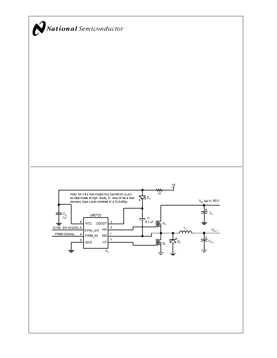
Typical Application
20028901
Note: National is an Intel Mobile Voltage Positioning (IMVP) licensee.
December 2001
LM2722
High
Speed
Synchronous/Asynchronous
MOSFET
Driver
© 2001 National Semiconductor Corporation
DS200289
www.national.com

Connection Diagram
8-Lead Small Outline Package
20028902
Top View
Ordering Information
Order Number
Package Type
NSC Package Drawing
Supplied As
LM2722
LM2722M
M08A
95 Units/Rail
LM2722MX
2500 Units/Reel
Pin Description
Pin
Name
Function
1
SW
Top driver return. Should be connected to the common node of top
and bottom FETs
2
HG
Top gate drive output
3
CBOOT
Bootstrap. Accepts a bootstrap voltage for powering the high-side
driver
4
PWM_IN
Accepts a 5V-logic control signal
5
SYNC_EN
Low gate Enable
6
VCC
Connect to +5V supply
7
LG
Bottom gate drive output
8
GND
Ground
LM2722
www.national.com
2
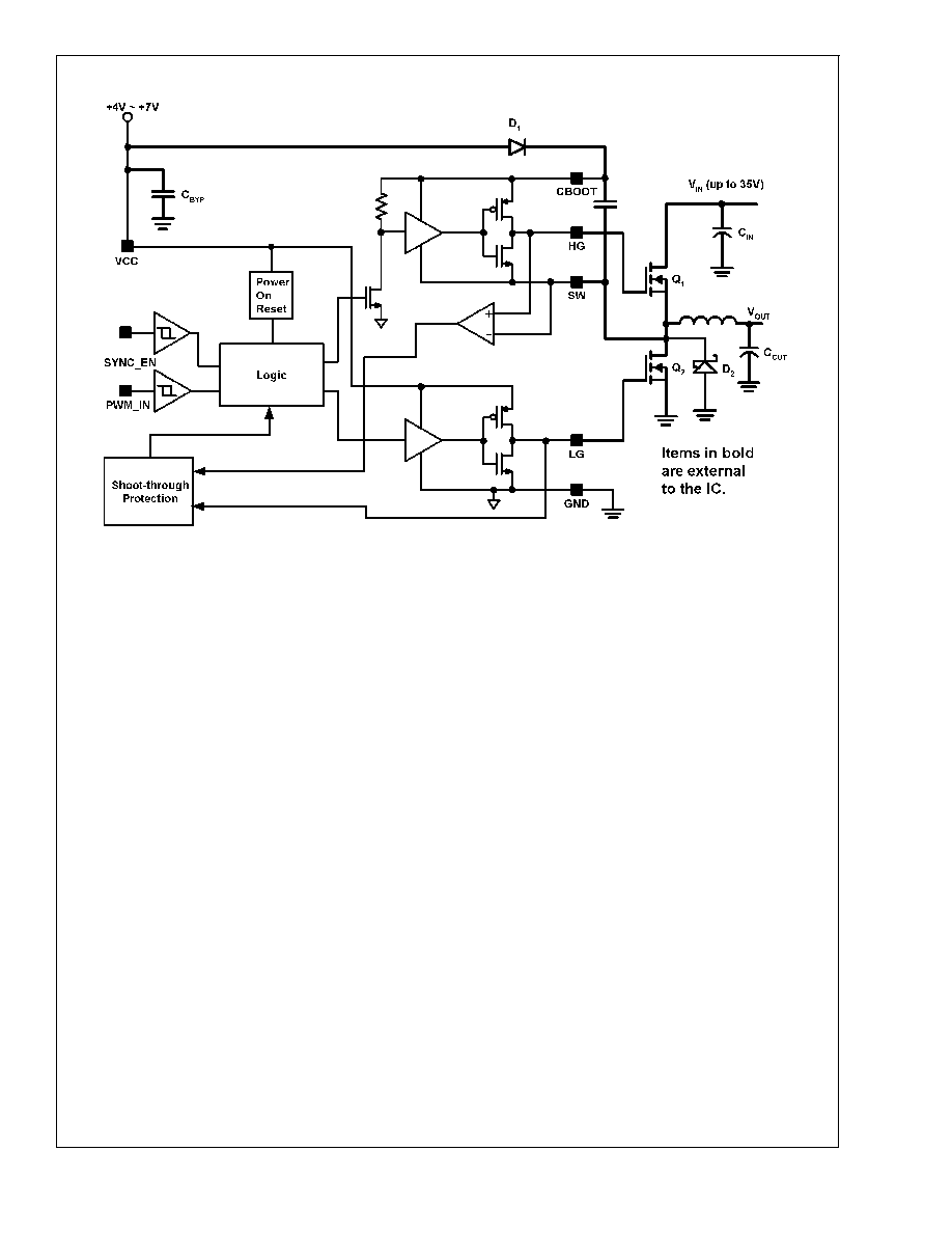
Block Diagram
20028904
LM2722
www.national.com
3

Absolute Maximum Ratings
(Note 1)
If Military/Aerospace specified devices are required,
please contact the National Semiconductor Sales Office/
Distributors for availability and specifications.
VCC
7.5V
CBOOT
42V
CBOOT to SW
8V
SW to PGND
36V
Junction Temperature
+150∞C
Power Dissipation
(Note 2)
720mW
Storage Temperature
-65∞ to 150∞C
ESD Susceptibility
Human Body Model (Note 3)
1kV
Soldering Time, Temperature
10sec., 300∞C
Operating Ratings
(Note 1)
VCC
4V to 7V
Junction Temperature Range
-40∞ to 125∞C
Electrical Characteristics
VCC = CBOOT = 5V, SW = GND = 0V, unless otherwise specified. Typicals and limits appearing in plain type apply for T
A
=
T
J
= +25∞C. Limits appearing in boldface type apply over the entire operating temperature range.
Symbol
Parameter
Condition
Min
Typ
Max
Units
POWER SUPPLY
I
q_op
Operating Quiescent
Current
PWM_IN = 0V
190
300
µA
TOP DRIVER
Peak Pull-Up Current
Test Circuit 1, V
bias
= 5V, R
= 0.1
3.0
A
Pull-Up Rds_on
I
CBOOT
= I
HG
= 0.7A
1.0
Peak Pull-down Current
Test Circuit 2, V
bias
= 5V, R
= 0.1
-3.2
A
Pull-down Rds_on
I
SW
= I
HG
= 0.7A
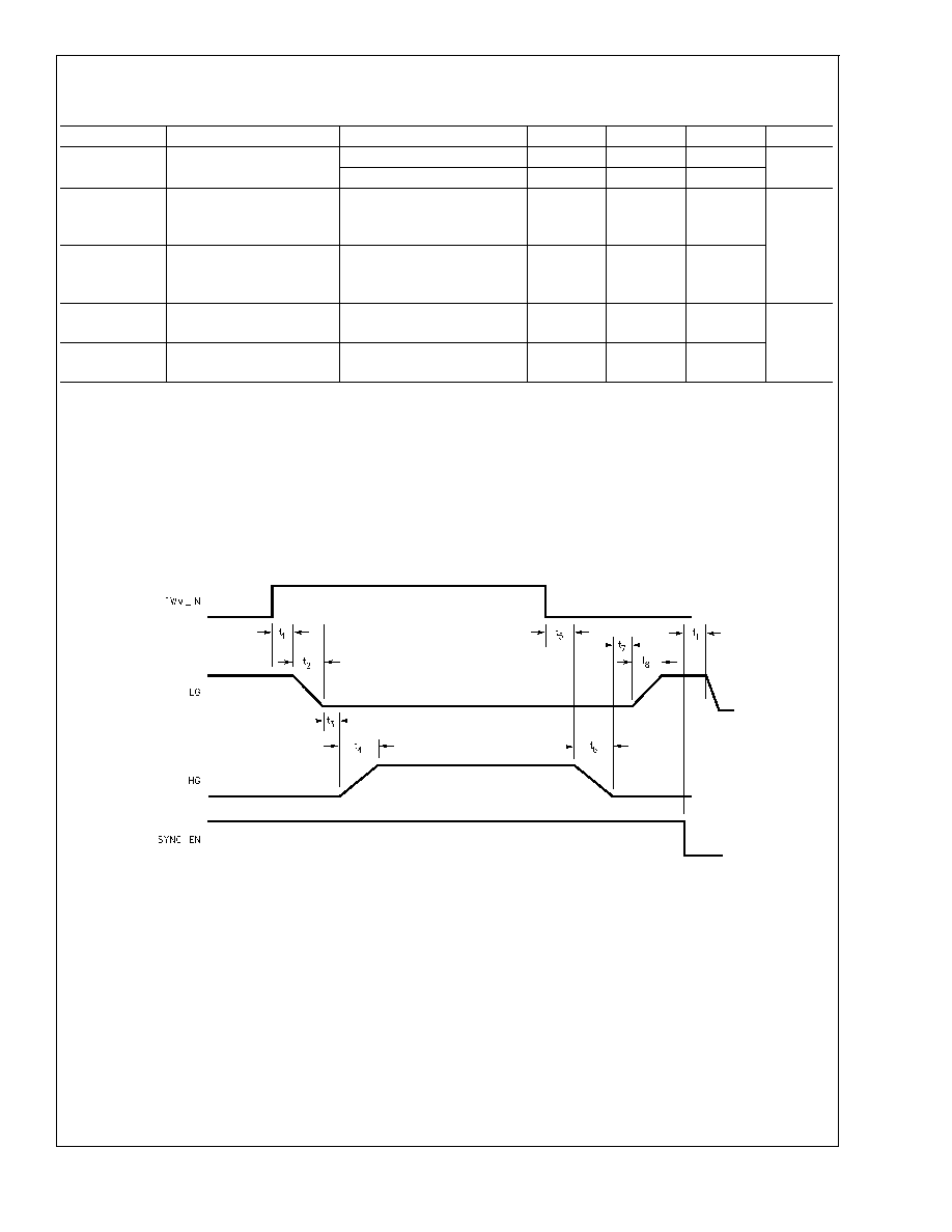
0.5
t
4
Rise Time
Timing Diagram, C
LOAD
=
3.3nF
17
ns
t
6
Fall Time
12
ns
t
3
Pull-Up Dead Time
Timing Diagram
23
ns
t
5
Pull-Down Delay
Timing Diagram, from
PWM_IN Falling Edge
27
ns
BOTTOM DRIVER
Peak Pull-Up Current
Test Circuit 3, V
bias
= 5V, R
= 0.1
3.2
A
Pull-up Rds_on
I
VCC
= I
LG
= 0.7A
1.0
Peak Pull-down Current
Test Circuit 4, V
bias
= 5V, R
= 0.1
3.2
A
Pull-down Rds_on
I
GND
= I
LG
= 0.7A
0.5
t
8
Rise Time
Timing Diagram, C
LOAD
=
3.3nF
17
ns
t
2
Fall Time
14
ns
t
7
Pull-up Dead Time
Timing Diagram
28
ns
t
1
Pull-down Delay
Timing Diagram, from
PWM_IN Rising Edge
13
ns
LOGIC
V
uvlo_up
Power On Threshold
VCC rises from 0V toward
5V
4
3.7
V
V
uvlo_dn
Under-Voltage-Lock-Out
Threshold
3.0
2.5
V
V
uvlo_hys
Under-Voltage-Lock-Out
Hysteresis
0.7
V
V
IH_EN
SYNC_EN Pin High Input
2.4
V
V
IL_EN
SYNC_EN Pin Low Input
0.8
V
LM2722
www.national.com
4
Electrical Characteristics
(Continued)
VCC = CBOOT = 5V, SW = GND = 0V, unless otherwise specified. Typicals and limits appearing in plain type apply for T
A
=
T
J
= +25∞C. Limits appearing in boldface type apply over the entire operating temperature range.
Symbol
Parameter
Condition
Min
Typ
Max
Units
I
leak_EN
SYNC_EN Pin Leakage
Current
EN = 5V
-2
2
µA
EN = 0V
-2
2
t
on_min
Minimum Positive Input
Pulse Width
(Note 4)
55
ns
t
off_min
Minimum Negative Input
Pulse Width
(Note 5)
55
V
IH_PWM
PWM_IN High Level Input
Voltage
When PWM_IN pin goes
high from 0V
2.4
V
V
IL_PWM
PWM_IN Low Level Input
Voltage
When PWM_IN pin goes
low from 5V
0.8
Note 1: Absolute Maximum Ratings are limits beyond which damage to the device may occur. Operating ratings are conditions under which the device operates
correctly. Operating Ratings do not imply guaranteed performance limits.
Note 2: Maximum allowable power dissipation is a function of the maximum junction temperature, T
JMAX
, the junction-to-ambient thermal resistance,
JA
, and the
ambient temperature, T
A
. The maximum allowable power dissipation at any ambient temperature is calculated using: P
MAX
= (T
JMAX
-T
A
) /
JA
. The junction-to-
ambient thermal resistance,
JA
, for the LM2722, it is 172∞C/W. For a T
JMAX
of 150∞C and T
A
of 25∞C, the maximum allowable power dissipation is 0.7W.
Note 3: ESD machine model susceptibility is 100V.
Note 4: If after a rising edge, a falling edge occurs sooner than the specified value, the IC may intermittently fail to turn on the bottom gate when the top gate is
off. As the falling edge occurs sooner and sooner, the driver may start to ignore the pulse and produce no output.
Note 5: If after a falling edge, a rising edge occurs sooner than the specified value, the IC may intermittently fail to turn on the top gate when the bottom gate is
off. As the rising edge occurs sooner and sooner, the driver may start to ignore the pulse and produce no output.
Timing Diagram
20028903
LM2722
www.national.com
5