LM27241
Synchronous Buck Regulator Controller for Mobile
Systems
General Description
The LM27241 is an adjustable 200kHz-500kHz single chan-
nel voltage-mode controlled high-speed synchronous buck
regulator controller. It is ideally suited for battery powered
applications such as laptop and notebook computers. The
LM27241 requires only N-channel FETs for both the upper
and lower positions of the synchronous stage. It features line
feedforward to improve the response to input transients. At
very light loads, the user can choose between the high-
efficiency Pulse-skip mode or the constant frequency
Forced-PWM mode. Lossless current limiting without the use
of external sense resistor is made possible by sensing the
voltage drop across the bottom FET. A unique adaptive duty
cycle clamping technique is incorporated to significantly re-
duce peak currents under abnormal load conditions. The
input voltage range is 5.5V to 28V while the output voltage is
adjustable down to 0.6V.
Standard supervisory and control features include soft-start,
power good, output under-voltage and over-voltage protec-
tion, under-voltage lockout, soft-shutdown and enable.
Features
n
Input voltage range from 5.5V to 28V
n
Forced-PWM or Pulse-skip modes
n
Lossless bottom-side FET current sensing
n
Adaptive duty cycle clamping
n
High current N-channel FET drivers
n
Low shutdown supply currents
n
Reference voltage accurate to within
±
1.5%
n
Output voltage adjustable down to 0.6V
n
Power Good flag and Chip Enable
n
Under-voltage lockout
n
Over-voltage/Under-voltage protection
n
Soft-start and Soft-shutdown
n
Switching frequency adjustable 200kHz-500kHz
Applications
n
Notebook Chipset Power Supplies
n
Low Output Voltage High Efficiency Buck Regulators
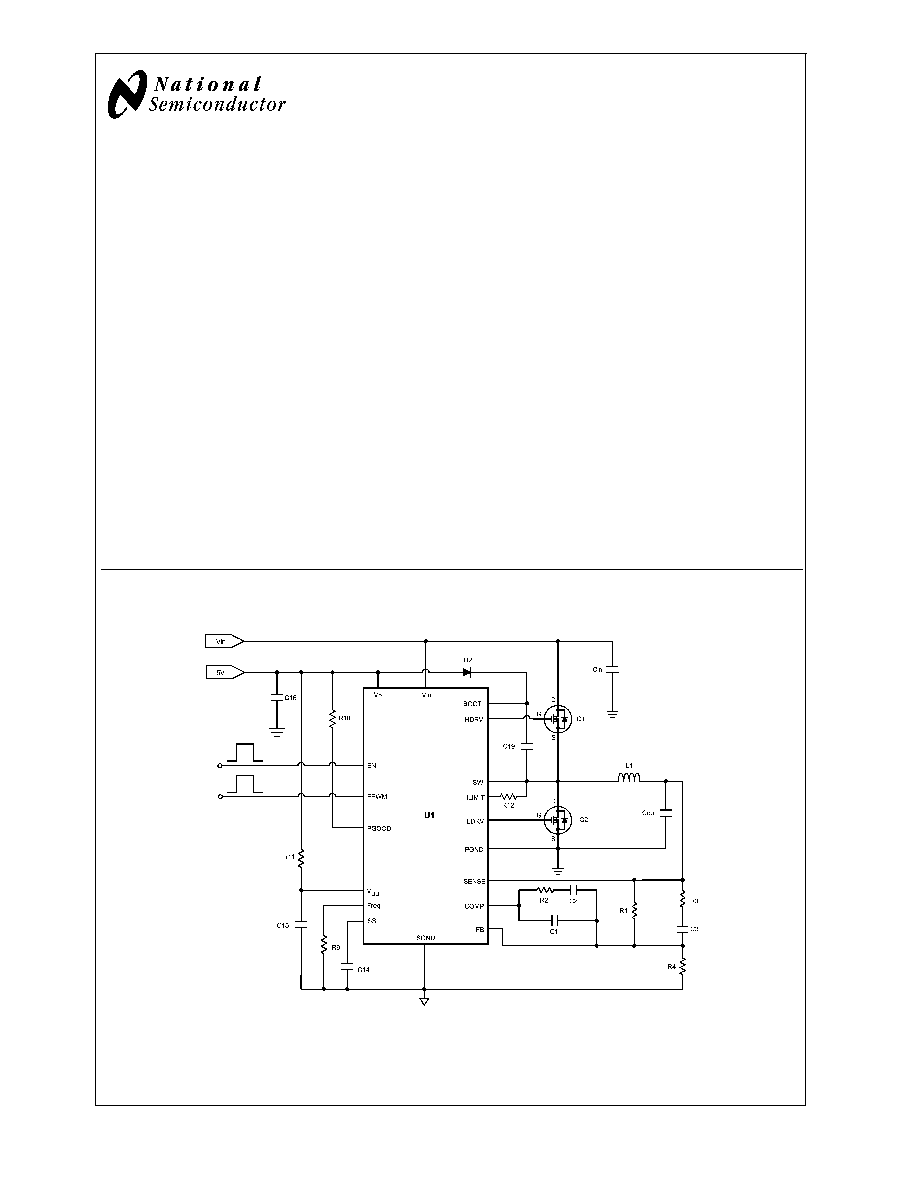
Typical Application
See Figure 17 for Expanded View
20120104
May 2005
LM27241
Synchronous
Buck
Regulator
Controller
for
Mobile
Systems
© 2005 National Semiconductor Corporation
DS201201
www.national.com
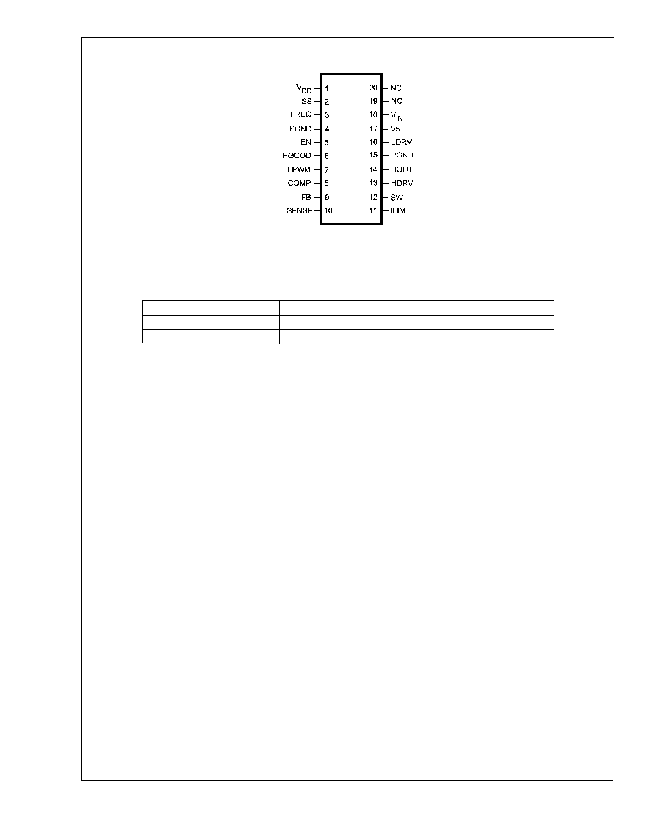
Connection Diagram
20120102
Top View
20-Lead TSSOP (MTC)
Ordering Information
Order Number
Package Drawing
Supplied As
LM27241MTC
MTC20
73 Units/Rail
LM27241MTCX
MTC20
2500 Units/13" Reel
Pin Description
Pin 1, VDD: 5V supply rail for the control and logic sections.
For normal operation the voltage on this pin must be brought
above 4.5V. Subsequently, the voltage on this pin (including
any ripple component) should not be allowed to fall below 4V
for a duration longer than 7µs. Since this pin is also the
supply rail for the internal control sections, it should be
well-decoupled particularly at high frequencies. A minimum
0.1µF-0.47µF (ceramic) capacitor should be placed on the
component side very close to the IC with no intervening vias
between this capacitor and the VDD/SGND pins. If the volt-
age on Pin 1 falls below the lower UVLO threshold, upper
FET(s) are latched OFF and the lower FET(s) are latched
ON. Power Not Good is then signaled immediately (on Pin
6). To initiate recovery, the EN pin must be taken below 0.8V
and then back above 2V (with VDD held above 4.5V). Or the
voltage on the VDD pin must be taken below 1.0V and then
back again above 4.5V (with EN pin held above 2V). Normal
operation will then resume assuming that the fault condition
has been cleared.
Pin 2, SS: Soft-start pin. A Soft-start capacitor is placed
between this pin and ground. A typical capacitance of 0.1µF
is recommended between this pin and ground. The IC con-
nects an internal 1.8 k
resistor (R
SS_DCHG
, see Electrical
Characteristics table) between this pin and ground to dis-
charge any remaining charge on the Soft-start capacitor
under several conditions. These conditions include the initial
power-up sequence, start-up by toggling the EN pin, and
also recovery from a fault condition. The purpose is to bring
down the voltage on the Soft-start pin to below 100mV for
obtaining reset. Reset having thus been obtained, an 11µA
current source at this pin charges up the Soft-start capacitor.
The voltage on this pin controls the maximum duty cycle,
and this produces a gradual ramp-up of the output voltage,
thereby preventing large inrush currents into the output ca-
pacitors. The voltage on this pin finally clamps close to 5V.
This pin is connected to an internal 115µA current sink
whenever a current limit event is in progress. This sink
current discharges the Soft-start capacitor and forces the
duty cycle low to protect the power components. When a
fault condition is asserted (See Pin 9) the SS pin is internally
connected to ground via the 1.8 k
resistor.
Pin 3, FREQ: Frequency adjust pin. The switching frequency
is set by a resistor connected between this pin and ground.
A value of 22.1k
sets the frequency to 300kHz (nominal). If
the resistance is increased, the switching frequency de-
creases. An approximate relationship is that for every 7.3k
increase or decrease in the value of the frequency set resis-
tor, the total switching period increases or decreases by 1µs.
Pin 4, SGND: Signal Ground pin. This is the lower rail for the
control and logic sections. SGND should be connected on
the PCB to the system ground, which in turn is connected to
PGND. The layout is important and the recommendations in
the section Layout Guidelines should be followed.
Pin 5, EN: IC Enable pin. When EN is taken high, the output
is enabled by means of a Soft-start power-up sequence.
When EN is brought low, Power Not Good is signaled within
100ns. This causes Soft-shutdown to occur (see Pins 2 and
6). The Soft-start capacitor is then discharged by an internal
1.8k
resistor (R
SS_DCHG
, see Electrical Characteristics
table). When the Enable pin is toggled, a fault condition is
not asserted. Therefore in this case, the lower FET is not
latched ON, even as the output voltage ramps down, even-
tually falling below the under-voltage threshold. In fact, in
this situation, both the upper and the lower FETs are latched
OFF, until the Enable pin is taken high again. If a fault
shutdown has occurred, taking the Enable pin low and then
high again (toggling), resets the internal latches, and the IC
will resume normal switching operation.
Pin 6, PGOOD: Power Good output pin. An open-drain logic
output that is pulled high with an external pull-up resistor,
indicating that the output voltage is within a pre-defined
Power Good window. Outside this window, the pin is inter-
nally pulled low (Power Not Good signaled) provided the
output error lasts for more than 7µs. The pin is also pulled
low within 100ns of the Enable pin being taken low, irrespec-
LM27241
www.national.com
2

Pin Description
(Continued)
tive of the output voltage level. PGOOD must always first be
"high" before it can respond to a proper fault "low" condition.
Under fault assertion, the low-side MOSFET is always
latched ON. This will not happen if regulation has not already
been achieved.
Pin 7, FPWM: Logic input for selecting either the Forced
PWM (FPWM) Mode or Pulse-skip Mode (SKIP). When the
pin is driven high, the IC operates in the FPWM mode, and
when pulled low or left floating, the SKIP mode is enabled. In
FPWM mode, the lower FET is always ON whenever the
upper FET is OFF (except for a narrow shoot-through pro-
tection deadband). This leads to continuous conduction
mode of operation, which has a fixed frequency and (almost)
fixed duty cycle down to very light loads. But this does
reduce efficiency at light loads. The alternative mode is SKIP
mode. This mode forces the lower MOSFET ON only until
the voltage on the Switch pin is more negative than 2.2mV
(typical). As an example, for a 21m
FET, this translates to
a current threshold of 2.2mV/21m
= 0.1A. Therefore, if the
(instantaneous) inductor current falls below this value, the
lower FET will turn OFF every cycle at this point (when
operated in SKIP mode). This threshold is set by the zero-
cross Comparator in the Block Diagram. Note that if the
inductor current is high enough to be always above this
zero-cross threshold (V
SW_ZERO
, see Electrical Characteris-
tics table), there will be no observable difference between
FPWM and SKIP mode settings (in steady-state). SKIP
mode is clearly a discontinuous mode of operation. How-
ever, in conventional discontinuous mode, the duty cycle
keeps falling (towards zero) as the load decreases. But the
LM27241 does not allow the duty cycle to fall by more than
15% of its original value (at the CCM-DCM boundary). This
forces pulse-skipping, and the average frequency is effec-
tively decreased as the load decreases. This mode of opera-
tion improves efficiency at light loads, but the frequency is
effectively no longer a constant. Note that a minimum pre-
load of 0.1mA should be maintained on the output to ensure
regulation in SKIP mode. The resistive divider from output to
ground used to set the output voltage could be designed to
serve as part or all of this required pre-load.
Pin 8, COMP: Compensation pin. This is also the output of
the error amplifier. The voltage level on this pin is compared
with an internally generated ramp signal to set the duty cycle
for normal regulation. Since the Feedback pin is the inverting
input of the same error amplifier, appropriate control loop
compensation components are placed between this pin and
the Feedback pin. The COMP pin is internally pulled low
during Soft-start so as to limit the duty cycle. Once Soft-start
is completed, the voltage on this pin can take up the value
required to maintain output regulation. An internal voltage
clamp at this pin forms an adaptive duty cycle clamp feature.
This serves to limit the maximum allowable duty cycles and
peak currents under sudden overloads. But at the same time
it has enough headroom to permit an adequate response to
step loads within the normal operating range.
Pin 9, FB: Feedback pin. This is the inverting input of the
error amplifier. The voltage on this pin under regulation is
nominally at 0.6V. A Power Good window on this pin deter-
mines if the output voltage is within regulation limits (
±
13%).
If the voltage falls outside this window for more than 7µs,
Power Not Good is signaled on the PGOOD pin (Pin 6).
Output over-voltage and under-voltage conditions are also
detected by comparing the voltage on the Feedback pin with
appropriate internal reference voltage levels. If the voltage
exceeds the safe window (
±
30%) for longer than 7µs, a fault
condition is asserted. Then lower FET is latched ON and the
upper FET is latched OFF.
Pin 10, SENSE: Output voltage sense pin. It is tied directly
to the output rail. The SENSE pin voltage is used together
with the VIN voltage (on Pin 18) to (internally) calculate the
CCM (continuous conduction mode) duty cycle. This calcu-
lation is used by the IC to set the minimum duty cycle in the
SKIP mode to 85% of the CCM value. It is also used to set
the adaptive duty cycle clamp. An internal 20
resistor from
the SENSE pin to ground discharges the output capacitor
gently (Soft-shutdown) whenever Power Not Good is sig-
naled on Pin 6.
Pin 11, ILIM: Current Limit pin. When the bottom FET is ON,
a 62µA (typical) current flows out of the ILIM pin and into an
external resistor that is connected to the drain of the lower
MOSFET. This current through the resistor creates a voltage
on the ILIM pin. However, the drain voltage of the lower
MOSFET will go more negative as the load current is in-
creased through the R
DS_ON
of the MOSFET. At some value
of instantaneous current, the voltage on this pin will transit
from positive to negative. The point where it is zero is the
current limiting condition and is detected by the Current Limit
Comparator. When a current limit condition has been de-
tected, the next ON-pulse of the upper FET will be omitted.
The lower FET will again be monitored to determine if the
current has fallen below the threshold. If it has, the next
ON-pulse will be permitted. If not, the upper FET will be
turned OFF and will stay so for several cycles if necessary,
until the current returns to normal. Eventually, if the overcur-
rent condition persists, and the upper FET has not been
turned ON, the output will clearly start to fall. Ultimately the
output will fall below the under-voltage threshold, and a fault
condition will be asserted by the IC.
Pin 12, SW: The Switching node of the buck regulator. Also
serves as the lower rail of the floating driver of the upper
FET.
Pin 13, HDRV: Gate drive pin for the upper FET. The top
gate driver is interlocked with the bottom gate driver to
prevent shoot-through/cross-conduction.
Pin 14, BOOT: Bootstrap pin. This is the upper supply rail for
the floating driver of the upper FET. It is bootstrapped by
means of a ceramic capacitor connected to the channel
Switching node. This capacitor is charged up by the IC to a
value of about 5V as derived from the V5 pin (Pin 17).
Pin 15, PGND: Power Ground pin. This is the return path for
the bottom FET gate drive. The PGND is to be connected on
the PCB to the system ground and also to the Signal ground
(Pin 4) in accordance with the recommended Layout Guide-
lines .
Pin 16, LDRV: Gate drive pin for the bottom FET (Low-side
drive). The bottom gate driver is interlocked with the top gate
driver to prevent shoot-through/cross-conduction. It is al-
ways latched high when a fault condition is asserted by the
IC.
Pin 17, V5: Upper rail of the lower FET driver. Also used to
charge up the bootstrap capacitor of the upper FET driver.
This is connected to an external 5V supply. The 5V rail may
be the same as the rail used to provide power to the VDD pin
(Pin 1), but the VDD pin will then require to be well-
decoupled so that it does not interact with the V5 pin. A
low-pass RC filter consisting of a ceramic 0.1µF capacitor
(preferably 0.22µF) and a 10
resistor will suffice as shown
in the Typical Applications circuit.
Pin 18, VIN: The input to the Buck regulator power stage. It
is also used by the internal ramp generator to implement the
LM27241
www.national.com
3

Pin Description
(Continued)
line feedforward feature. The VIN pin is also used with the
SENSE pin voltage to predict the CCM (continuous conduc-
tion mode) duty cycle and to thereby set the minimum al-
lowed DCM duty cycle to 85% of the CCM value. This is a
high input impedance pin, drawing only about 100µA (typi-
cal) from the input rail.
Pin 19, 20 NC: No Connect.
LM27241
www.national.com
4
Absolute Maximum Ratings
(Note 1)
If Military/Aerospace specified devices are required,
please contact the National Semiconductor Sales Office/
Distributors for availability and specifications.
Voltages from the indicated pins to SGND/PGND unless
otherwise indicated (Note 2):
VIN
-0.3V to 30V
V5
-0.3V to 7V
VDD
-0.3V to 7V
BOOT
-0.3V to 36V
BOOT to SW
-0.3V to 7V
SW
-0.3V to 30V
ILIM
-0.3V to 30V
SENSE, FB
-0.3V to 7V
PGOOD
-0.3V to 7V
EN
-0.3V to 7V
Power Dissipation (T
A
= 25∞C)
(Note 3)
0.75W
Junction Temperature
+150∞C
ESD Rating (Note 4)
2kV
Ambient Storage Temperature
Range
-65∞C to +150∞C
Soldering Dwell Time,
Temperature
Wave
Infrared
Vapor Phase
4 sec, 260∞C
10 sec, 240∞C
75 sec, 219∞C
Operating Ratings
(Note 1)
VIN
5.5V to 28V
VDD, V5
4.5V to 5.5V
Junction Temperature
-5∞C to +125∞C
Electrical Characteristics
Specifications with standard typeface are for T
J
= 25∞C, and those with boldface apply over full Operating Junction Tempera-
ture range. VDD = V5 = 5V, V
SGND
= V
PGND
= 0V, VIN = 15V, V
EN
= 3V, R
FADJ
= 22.1K unless otherwise stated (Note 5).
Datasheet min/max specification limits are guaranteed by design, test, or statistical analysis.
Symbol
Parameter
Conditions
Min
Typical
(Note 7)
Max
Units
Reference
V
FB_REG
FB Pin Voltage at
Regualtion
VDD = 4.5V to 5.5V,
VIN = 5.5V to 28V
591
600
609
mV
V
FB_LINE REG
V
FB
Line Regulation
VDD = 4.5V to 5.5V,
VIN = 5.5V to 28V
0.5
I
FB
FB Pin Current (sourcing)
V
FB
at regulation
20
100
nA
Chip Supply
I
Q_VIN
VIN Quiescent Current
V
FB
= 0.7V
100
200
µA
I
SD_VIN
VIN Shutdown Current
V
EN
= 0V
0
5
µA
I
Q_VDD
VDD Quiescent Current
V
FB
= 0.7V
1.75
3
mA
I
SD_VDD
VDD Shutdown Current
V
EN
= 0V
8
15
µA
I
Q_V5
V5 Normal Operating
Current
V
FB
= 0.7V
0.3
0.5
mA
V
FB
= 0.5V
0.5
1.25
I
SD_V5
V5 Shutdown Current
V
EN
= 0V
0
5
µA
I
Q_BOOT
BOOT Quiescent Current
V
FB
= 0.7V
2
5
µA
V
FB
= 0.5V
300
500
I
SD_BOOT
BOOT Shutdown Current
V
EN
= 0V
1
5
µA
V
DD_UVLO
VDD UVLO Threshold
VDD rising from 0V
3.9
4.2
4.5
V
HYS
VDD_UVLO
VDD UVLO Hysteresis
VDD = V5 falling from
V
DD_UVLO
0.5
0.7
0.9
V
Logic
I
EN
EN Input Current
V
EN
= 0 to 5V
0
µA
V
EN_HI
EN Input Logic High
2
1.8
V
V
EN_LO
EN Input Logic Low
1.3
0.8
V
R
FPWM
FPWM Pull-down
V
FPWM
= 2V
100
200
1000
k
V
FPWM_HI
FPWM Input Logic High
2
1.8
V
VFPWM_LO
FPWM Input Logic Low
1.3
0.8
V
LM27241
www.national.com
5