LM2724A
High Speed 3A Synchronous MOSFET Driver
General Description
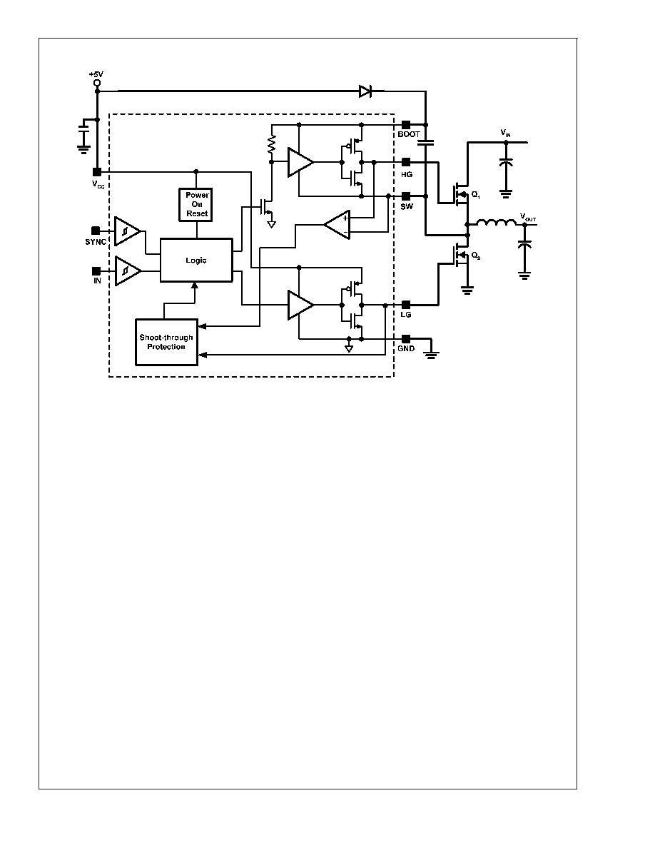
The LM2724A is a dual N-channel MOSFET driver which
can drive both the top and bottom MOSFETs in a push-pull
structure simultaneously. The LM2724A takes a logic input
and splits it into two complimentary signals with a typical
20ns dead time in between. The built-in cross-conduction
protection circuitry prevents the top and bottom MOSFETs
from turning on simultaneously. With a bias voltage of 5V, the
peak sourcing and sinking current for each driver of the
LM2724A is about 3A. Input UVLO (Under-Voltage-Lock-
Out) ensures that all the driver outputs stay low until the
supply rail exceeds the power-on threshold during system
power on, or after the supply rail drops below power-on
threshold by a specified hysteresis during system power
down. The cross-conduction protection circuitry detects both
driver outputs and will not turn on a driver until the other
driver output is low. The top gate voltage needed by the top
MOSFET is obtained through an external boot-strap struc-
ture. When not switching, the LM2724A only draws up to
195µA from the 5V rail. The synchronization operation of the
bottom MOSFET can be disabled by pulling the SYNC pin to
ground.
Features
n
Shoot-through protection
n
Input Under-Voltage-Lock-Out
n
3A peak driving current
n
195µA quiescent current
n
28V input voltage in buck configuration
n
SO-8 and LLP packages
Applications
n
High Current DC/DC Power Supplies
n
High Input Voltage Switching Regulators
n
Fast Transient Microprocessors
n
Notebook Computers
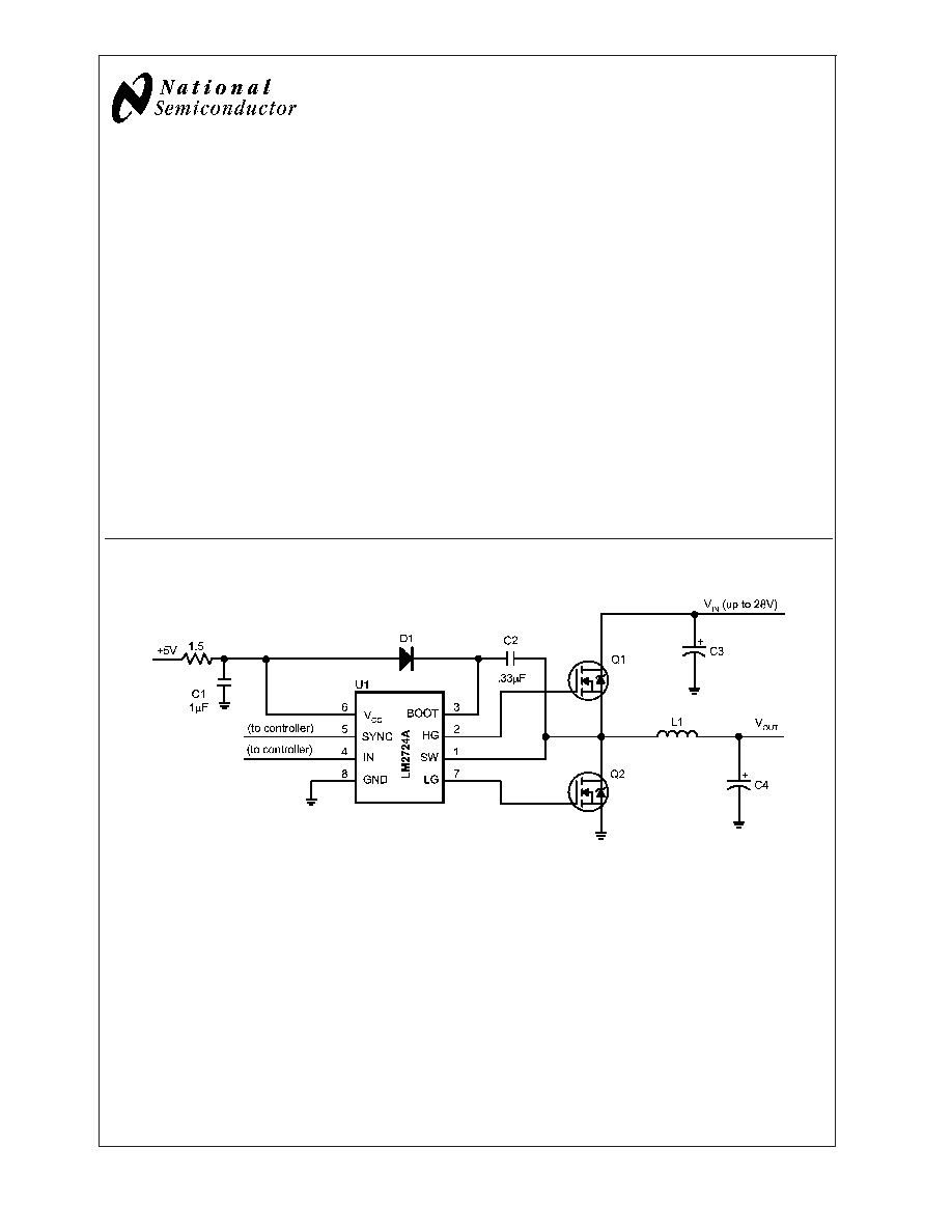
Typical Application
20073501
June 2003
LM2724A
High
Speed
3A
Synchronous
MOSFET
Driver
© 2003 National Semiconductor Corporation
DS200735
www.national.com
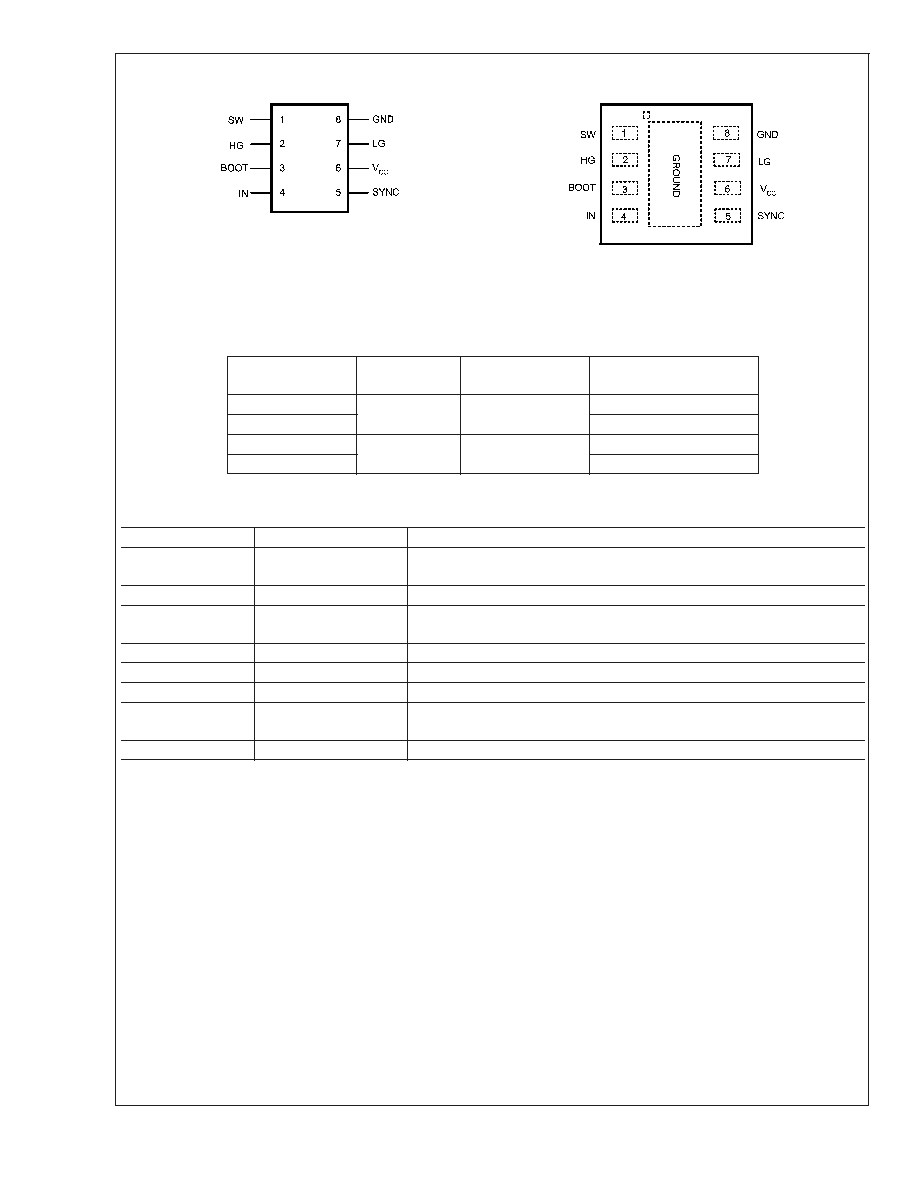
Connection Diagram
20073502
8-Lead SO (NS Package # M08A)
JA
= 172∞C/W
20073506
8-Lead LLP (NS Package # LDC08A)
JA
= 39∞C/W
Ordering Information
Order Number
Size
NSC Package
Drawing
Supplied As
LM2724AM
SO-8
M08A
95 Units/Rail
LM2724AMX
2500 Units/Reel
LM2724ALD
LDC08A
LDC08A
1000 Units/Rail
LM2724ALDX
4500 Units/Reel
Pin Descriptions
Pin
Name
Function
1
SW
Top driver return. Should be connected to the common node of top
and bottom FETs
2
HG
Top gate drive output. Should be connected to the top FET gate.
3
BOOT
Bootstrap. Accepts a bootstrap voltage for powering the high-side
driver
4
IN
Accepts a logic control signal
5
SYNC
Bottom gate enable
6
V
CC
Connect to +5V supply
7
LG
Bottom gate drive output. Should be connected to the bottom FET
gate.
8
GND
Ground
LM2724A
www.national.com
2
Absolute Maximum Ratings
(Note 1)
If Military/Aerospace specified devices are required,
please contact the National Semiconductor Sales Office/
Distributors for availability and specifications.
V
CC
7V
BOOT to SW
7V
BOOT to GND (Note 2)
35V
SW to GND
30V
Junction Temperature
+150∞C
Power Dissipation
(Note 3)
720mW (SO-8)
3.2W (LLP-8)
Storage Temperature
-65∞C to 150∞C
ESD Susceptibility
Human Body Model (Note 4)
2.0 kV
Soldering Time, Temperature
10sec., 300∞C
Operating Ratings
(Note 1)
V
CC
4.3V to 6.8V
Junction Temperature Range
-40∞C to 125∞C
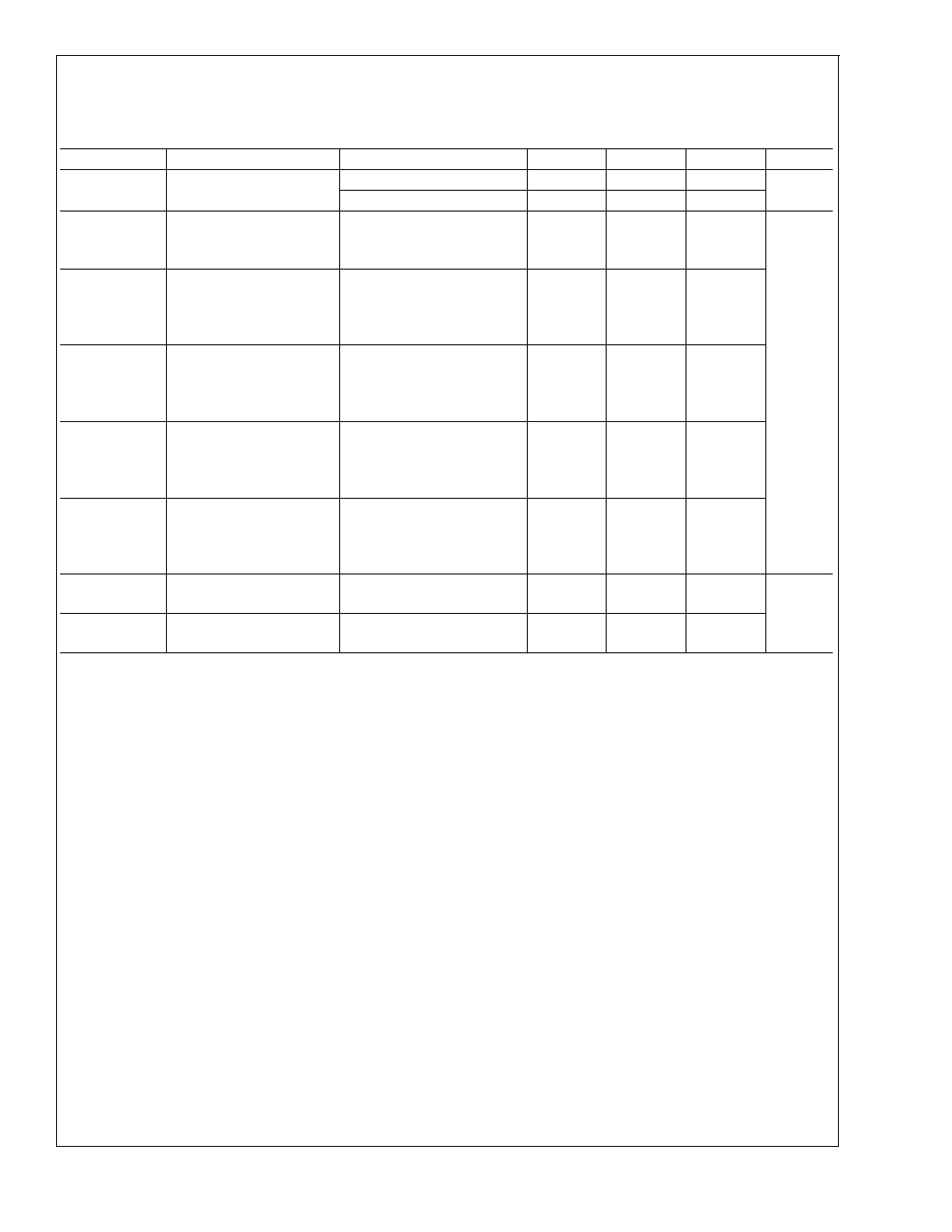
Electrical Characteristics
LM2724A
V
CC
= BOOT = SYNC = 5V, SW = GND = 0V, unless otherwise specified. Typicals and limits appearing in plain type apply for
T
A
= T
J
= +25∞C. Limits appearing in boldface type apply over the entire operating temperature range.
Symbol
Parameter
Condition
Min
Typ
Max
Units
POWER SUPPLY
I
q_op
Operating Quiescent
Current
IN = 0V
145
195
µA
TOP DRIVER
Peak Pull-Up Current
3.0
A
Pull-Up Rds_on
I
BOOT
= I
HG
= 0.3A
1.2
Peak Pull-down Current
-3.2
A
Pull-down Rds_on
I
SW
= I
HG
= 0.3A
0.5
t
4
Rise Time
Timing Diagram, C
LOAD
=
3.3nF
17
ns
t
6
Fall Time
12
ns
t
3
Pull-Up Dead Time
Timing Diagram
19
ns
t
5
Pull-Down Delay
Timing Diagram, from IN
Falling Edge
27
ns
BOTTOM DRIVER
Peak Pull-Up Current
3.2
A
Pull-up Rds_on
I
VCC
= I
LG
= 0.3A
1.1
Peak Pull-down Current
3.2
A
Pull-down Rds_on
I
GND
= I
LG
= 0.3A
0.6
t
8
Rise Time
Timing Diagram, C
LOAD
=
3.3nF
17
ns
t
2
Fall Time
14
ns
t
7
Pull-up Dead Time
Timing Diagram
22
ns
t
1
Pull-down Delay
Timing Diagram
13
ns
LOGIC
V
uvlo_up
V
CC
Under-Voltage-Lock-Out
Upper Threshold
V
CC
rises from 0V toward
5V
4
V
V
uvlo_dn
V
CC
Under-Voltage-Lock-Out
Lower Threshold
VCC falls from 5V toward
0V
2.5
V
V
uvlo_hys
V
CC
Under-Voltage-Lock-Out
Hysteresis
V
CC
falls from 5V toward 0V
0.8
V
V
IH_SYNC
SYNC Pin High Input
55%
V
CC
V
IL_SYNC
SYNC Pin Low Input
25%
I
leak_SYNC
SYNC Pin Leakage
Current
SYNC = 5V, Sink Current
2
µA
SYNC = 0V, Source Current
10
LM2724A
www.national.com
4
Electrical Characteristics
LM2724A
(Continued)
V
CC
= BOOT = SYNC = 5V, SW = GND = 0V, unless otherwise specified. Typicals and limits appearing in plain type apply for
T
A
= T
J
= +25∞C. Limits appearing in boldface type apply over the entire operating temperature range.
Symbol
Parameter
Condition
Min
Typ
Max
Units
I
leak_IN
IN Pin Leakage Current
IN = 0V, Source Current
2
µA
IN = 5V, Sink Current
10
t
on_min1
Minimum Positive Pulse
Width at IN Pin
(Note 5)
160
ns
t
on_min2
Minimum Positive Pulse
Width at IN Pin for HG to
Respond
(Note 6)
45
t
on_min3
Minimum Positive Pulse
Width at IN Pin for LG to
Respond
(Note 7)
10
t
off_min1
Minimum Negative Pulse
Width at IN Pin for LG to
Respond
(Note 8)
40
t
off_min2
Minimum Negative Pulse
Width at IN Pin for HG to
Respond
(Note 9)
5
V
IH_IN
IN High Level Input
Voltage
When IN pin goes high from
0V
55%
V
CC
V
IL_IN
IN Low Level Input
Voltage
When IN pin goes low from
5V
25%
Note 1: Absolute Maximum Ratings are limits beyond which damage to the device may occur. Operating ratings are conditions under which the device operates
correctly. The gaurnteed specifications apply only for the listed test conditions. Some performance characteristics may degrade when the part is not operated under
listed conditions.
Note 2: If BOOT voltage exceeds this value, the ESD structure will degrade.
Note 3: Maximum allowable power dissipation is a function of the maximum junction temperature, T
JMAX
, the junction-to-ambient thermal resistance,
JA
, and the
ambient temperature, T
A
. The maximum allowable power dissipation at any ambient temperature is calculated using: P
MAX
= (T
JMAX
-T
A
) /
JA
. The junction-to-
ambient thermal resistance,
JA
, for LM2724A is 172∞C/W. For a T
JMAX
of 150∞C and T
A
of 25∞C, the maximum allowable power dissipation is 0.7W. The
JA
, for
LM2724A LLP package is 39∞C/W. For a T
JMAX
of 150∞C and T
A
of 25∞C, the maximum allowable power dissipation is 3.2W.
Note 4: ESD machine model susceptibility is 200V.
Note 5: If the positive pulse width at IN pin is below this value but above t
on_min2
, the pulse is internally stretched to t
on_min1
, so the HG width will be a constant
value.
Note 6: If the positive pulse width at IN pin is below this value but above t
on_min3
, then HG stops responding while LG still responds to the pulse.
Note 7: If the positive pulse width at IN pin is below this value, the pulse will be completely ignored. Neither HG or LG will respond to it.
Note 8: If the negative pulse width at IN pin is below this value but above t
off_min2
, then LG stops responding while HG still responds.
Note 9: If the negative pulse width at IN pin is below this value, the pulse will be completely ignored. Neither HG or LG will respond to it.
LM2724A
www.national.com
5