LM27262
Intel CPU Core Voltage Regulator Controller for VRD10
Compatible PCs
General Description
The LM27262 is a versatile synchronous buck voltage regu-
lator controller designed according to the Intel VRD10 Speci-
fication. It's a fixed-frequency voltage-mode control PWM
with average current modulation of the reference voltage to
achieve the desired output impedance. This approach im-
parts a pseudo current mode behavior to the control loop.
The part provides the control for a voltage regulator consist-
ing of either 2-, 3- or 4-phases to provide power to a desktop
CPU. Pulse-by-pulse phase current balancing ensures ac-
curate current sharing. CPU core currents of over 90A can
be supported without requiring significant over design of the
power path. The LM27262 contains a precision 6-bit digital-
to-analog converter (DAC) that uses a VID-code provided by
the CPU to program the desired CPU core voltage. The
regulator output voltage can be dynamically adjusted by
changing the VID-code "on the fly".
The part is intended to provide all the specified functions laid
out in the VRD-10 specification, making it as simple as
possible for the user to realize a fully compliant CPU core
supply for Intel's Pentium
TM
4 and Prescott
TM
processors.
The LM27262 is available in a 48-lead TSSOP package and
in a 48-lead LLP package.
Features
n
Compatible with "VRD10 Voltage Regulation
Specification" for Intel Pentium 4 and Prescott
Processors
n
Supports Intel SpeedStep
TM
technology
(Geyserville-III
TM
), which enables real-time dynamic
switching of the CPU core voltage and the CPU clock
frequency
n
Uses external gate drivers (LM2724) for maximum
layout flexibility and noise immunity
n
Fixed frequency PWM architecture
n
Pin selectable internal or external voltage reference
n
0.5% core voltage set-point accuracy when using
external voltage reference
n
0.9% accurate internal bandgap reference
n
2-, 3- or 4-phase operation
n
Out-of-phase switching reduces input ripple current,
thereby minimizing input capacitor requirements
n
VID-code programmable output voltage range of
0.8375V through 1.6000V
n
User programmable, low loss, load line slope
n
User programmable Standard VID offset
n
User programmable VCORE slew rate
n
5V power rail Under Voltage Lock Out (UVLO)
n
Over Voltage Protection (OVP), Under Voltage
Protection (UVP), and Over Current Protection (OCP) to
defend against potentially catastrophic events
n
User programmable fault latch that can be used to
disable the regulator in the event a power system fault
n
Very fast transient response
n
VID-transition masked PWRGOOD output
n
True-differential current sensing for each phase ensures
accurate load current sharing
n
User programmable cycle-by-cycle current limit
Key Specifications
n
Fast transient response to minimize output capacitor
requirements
n
Shorter design cycles through the use of external gate
drivers for reduced power dissipation, ease of PCB
layout and reduced noise sensitivity
n
Fully integrated solution. All VRD-10 control functions
provided by a single device
n
Accurate current balancing eliminates need to over
design the power path
n
Fixed frequency PWM minimizes EMI issues
n
Low input capacitor requirements due to multi-phase
interleaving
n
Fault latching allows use of smaller power path
components and minimizes the chance of damage to
the load in the event of a fault
n
Only need to buy as many drivers as the design needs
while keeping only one controller in inventory
Applications
n
Server and desktop computer CPU core power supplies
requiring a 2, 3- or 4-phase voltage regulator delivering
up to 100A
n
Transportable notebook computers using desktop CPUs
n
Low cost transportable notebook computers using 2- or
3-phase designs
Pentium
TM
is a trademark of Intel Corporation.
October 2004
LM27262
Intel
CPU
Core
V
oltage
Regulator
Controller
for
VRD10
Compatible
PCs
� 2005 National Semiconductor Corporation
DS200834
www.national.com

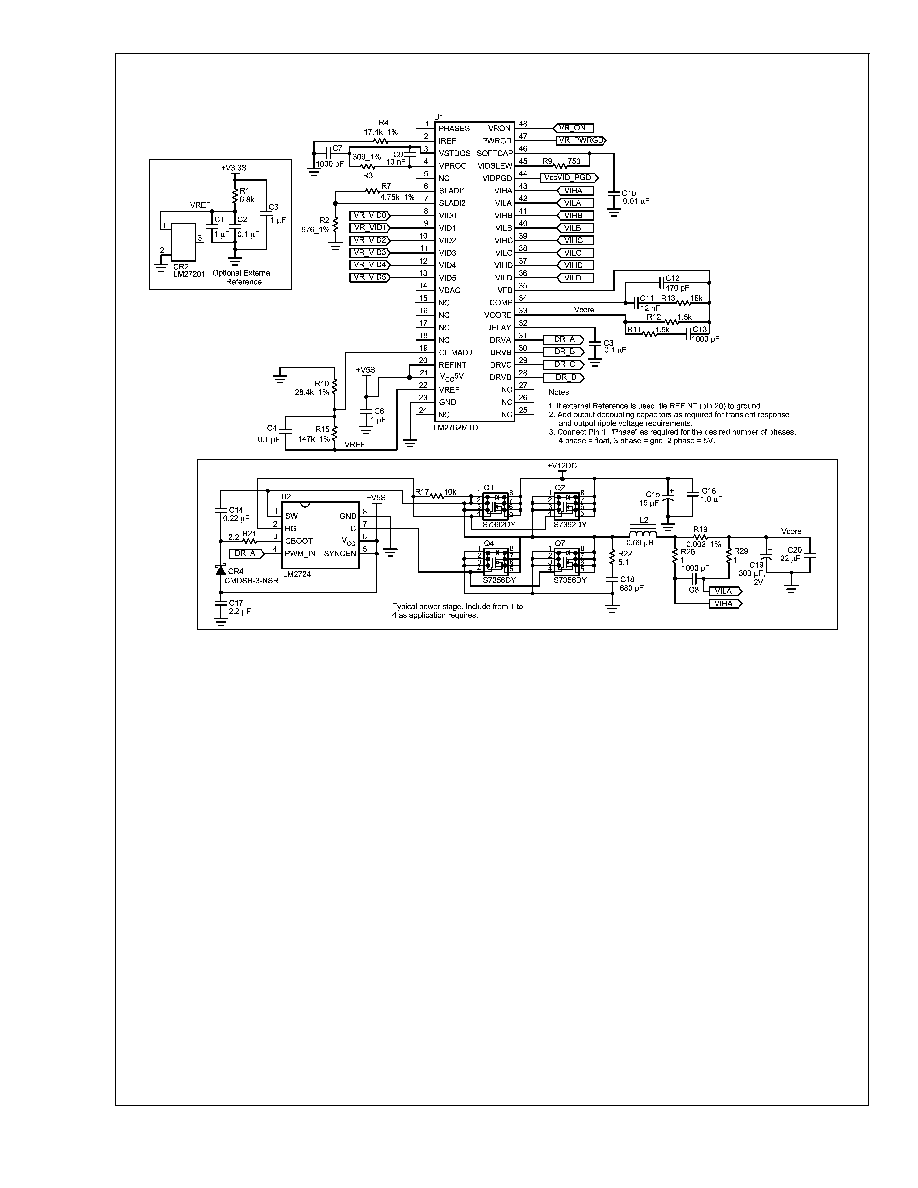
Pin Description
(All pin numbers referred to here correspond to the TSSOP/
LLP package)
Pin 1/44, PHASES: tri-level logic input: HIGH logic level
switches controller into 2-phase operation mode, phases A
and C active. LOW logic level activates 3-phase operation,
phases A, B and C active, OPEN (floating) input activates
4-phase operation
Pin 2/45, IREF: connect a 1% resistor to ground to program
a precision current source for a standard offset voltage,
typically �25mV, across a resistor connected between
VPROG and VSTDOS pins. Recommended current value is
approximately 80�A. Typical resistor value is R = 1.4V /
80�A equals 17.4k.
Pin 3/46, VSTDOS: input; V
VSTDOS
= V
VPROG
� V
OS
. This
pin allows setting a programmable offset voltage (typically
25mV). The offset is programmed via an external 1% resistor
connected between the VPROG and VSTDOS pins. The
offset is the Pin 2 current multiplied by this offset program-
ming resistor.
Pin 4/47, VPROG: output used for programming a standard
offset. Connect a 1% resistor between VPROG and VST-
DOS. VPROG output voltage is the buffered internal DAC
output.
Pin 5/48: No connect pin
Pin 6/1, SLADJ1: load line slope adjustment via external
resistor divider
Pin 7/2, SLADJ2: load line slope adjustment via external
resistor divider
Pin 8 � 13/3-8, VID0-VID5: voltage identification code inputs
Pin 14/9, VDAC: buffered output of onboard DAC. Voltage
determined by VID code.
Pin 15-18/10-13: no connect pin
Pin 19/14, CLIMADJ: output current limit adjustment input
for one phase. For 4-phase operation the current limit is 4x
the single phase current limit, for 3-phase operation it is 3x
the single phase limit, and 2x the single phase current for
2-phase operation
Pin 20/15, REFINT: internal/external voltage reference se-
lection logic input. When logic high, selects internal refer-
ence
Pin 21/16, VCC5V: 5V power supply input to the part.
Should be decoupled to GND pin with a 1uF capacitor.
Pin 22/17, VREF: internal voltage reference output or exter-
nal voltage reference input depending on REFINT input logic
state
Pin 23/18, GND: the chip ground pin. Use for 5V supply
ground connection, Make a single-point ground connection
at this pin.
Pin 24 � 27/19-22: no connect pins
Pin 28-31/23-26: DRIVED-DRIVEA: PWM logic level out-
puts for phases D through A. Not short-circuit protected.
Pin 32/27, DELAY: OVP, UVP and OCP latch-off delay
adjustment pin. A delay programming capacitor is connected
between this pin and ground. This pin disables UVP, OVP
and OCP latch-off when grounded to facilitate debugging
Pin 33/28, VCORE: CPU core voltage rail connection. This
pin is the OVP/UVP sense point.
Pin 34/29, COMP: output of error amplifier. Use for external
loop compensation connection
Pin 35/30, VFB: input of error amplifier. Use for external loop
compensation connection Pin 36/31, VILD: phase D current
sense resistor low-side connection input
Pin 37/32, VIHD: phase D current sense resistor high-side
connection input
Pin 38/33, VILC: phase C current sense resistor low-side
connection input
Pin 39/34, VIHC: phase C current sense resistor high-side
connection input
Pin 40/35, VILB: phase B current sense resistor low-side
connection input
Pin 41/36, VIHB: phase B current sense resistor high-side
connection input
Pin 42/37, VILA: phase A current sense resistor low-side
connection input
Pin 43/38, VIHA: phase A current sense resistor high-side
connection input
Pin 44/39, VIDPGD: VID Power Good Delayed output. Out-
puts a VID_PWRGD signal that is delayed approximately
2msec after receiving an externally supplied active high
signal to VRON. Pin VIDPGD should be connected to the
system's VID_PWRGD input. This delay ensures that Vcore
will power on only after the 6 VID bit signals have settled.
The LM27262 is only enabled after the delay has timed out.
Pin 45/40, VIDSLEW: connect a resistor between this pin
and the SOFTCAP pin to program VCORE slew rates for
VID transitions
Pin 46/41, SOFTCAP: soft start/soft stop capacitor connec-
tion; this output sources charging current to the softstart
capacitor at power on. An internal 50k resistor discharges
the softstart capacitor during power off
Pin 47/42, PWRGD: power good output, open drain, active
high
Pin 48/43, VRON: logic input that turns the switching regu-
lator on and off. If VCC5V is present when the LM27262 is
shutdown then the DRIVEx outputs are active low. VRON
has a 2msec assertion delay. When VRON is de-asserted,
the VID DAC latches the latest VID code and executes
soft-stop. There is no de-assertion delay on VRON.
LLP DAP, SUB: die substrate. The exposed die attach
should be connected to ground potentful.
LM27262
www.national.com
4