LM2731
0.6/1.6 MHz Boost Converters With 22V Internal FET
Switch in SOT-23
General Description
The LM2731 switching regulators are current-mode boost
converters operating at fixed frequencies of 1.6 MHz ("X"
option) and 600 kHz ("Y" option).
The use of SOT-23 package, made possible by the minimal
power loss of the internal 1.8A switch, and use of small
inductors and capacitors result in the industry's highest
power density. The 22V internal switch makes these solu-
tions perfect for boosting to voltages up to 20V.
These parts have a logic-level shutdown pin that can be
used to reduce quiescent current and extend battery life.
Protection is provided through cycle-by-cycle current limiting
and thermal shutdown. Internal compensation simplifies de-
sign and reduces component count.
Switch Frequency
X
Y
1.6 MHz
0.6 MHz
Features
n
22V DMOS FET switch
n
1.6 MHz ("X"), 0.6 MHz ("Y") switching frequency
n
Low R
DS
(ON) DMOS FET
n
Switch current up to 1.8A
n
Wide input voltage range (2.7V≠14V)
n
Low shutdown current (
<
1 µA)
n
5-Lead SOT-23 package
n
Uses tiny capacitors and inductors
n
Cycle-by-cycle current limiting
n
Internally compensated
Applications
n
White LED Current Source
n
PDA's and Palm-Top Computers
n
Digital Cameras
n
Portable Phones and Games
n
Local Boost Regulator
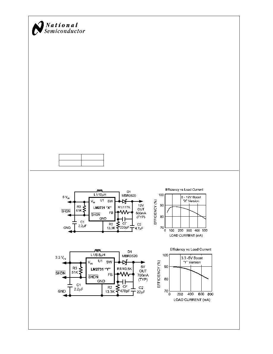
Typical Application Circuit
20059110
20059130
July 2003
LM2731
0.6/1.6
MHz
Boost
Converters
W
ith
22V
Internal
FET
Switch
in
SOT
-23
© 2003 National Semiconductor Corporation
DS200591
www.national.com
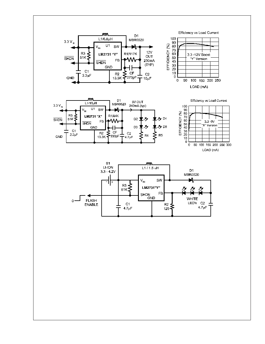
Typical Application Circuit
(Continued)
20059153
20059156
20059155
White LED Flash Application
LM2731
www.national.com
2
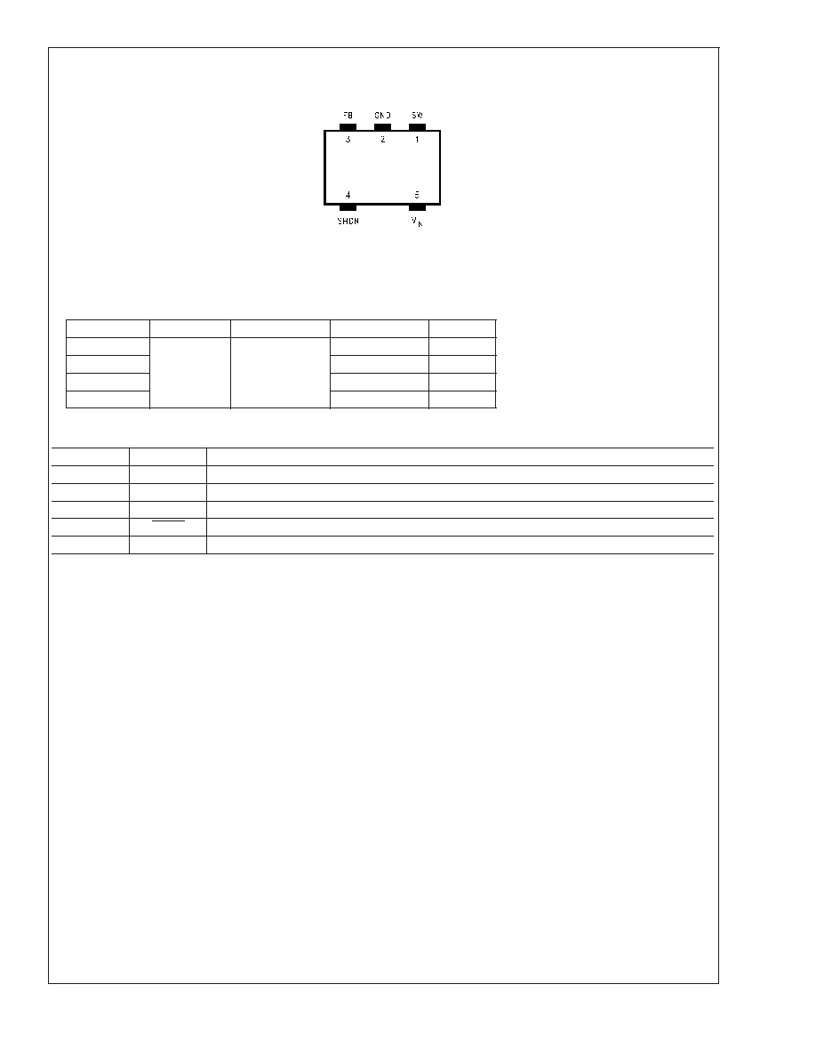
Connection Diagram
Top View
20059111
5-Lead SOT-23 Package
See NS Package Number MF05A
Ordering Information
Order Number Package Type Package Drawing
Supplied As
Package ID
LM2731XMF
SOT23-5
MF05A
1K Tape and Reel
S51A
LM2731XMFX
3K Tape and Reel
S51A
LM2731YMF
1K Tape and Reel
S51B
LM2731YMFX
3K Tape and Reel
S51B
Pin Description
Pin
Name
Function
1
SW
Drain of the internal FET switch.
2
GND
Analog and power ground.
3
FB
Feedback point that connects to external resistive divider.
4
SHDN
Shutdown control input. Connect to Vin if the feature is not used.
5
V
IN
Analog and power input.
LM2731
www.national.com
3
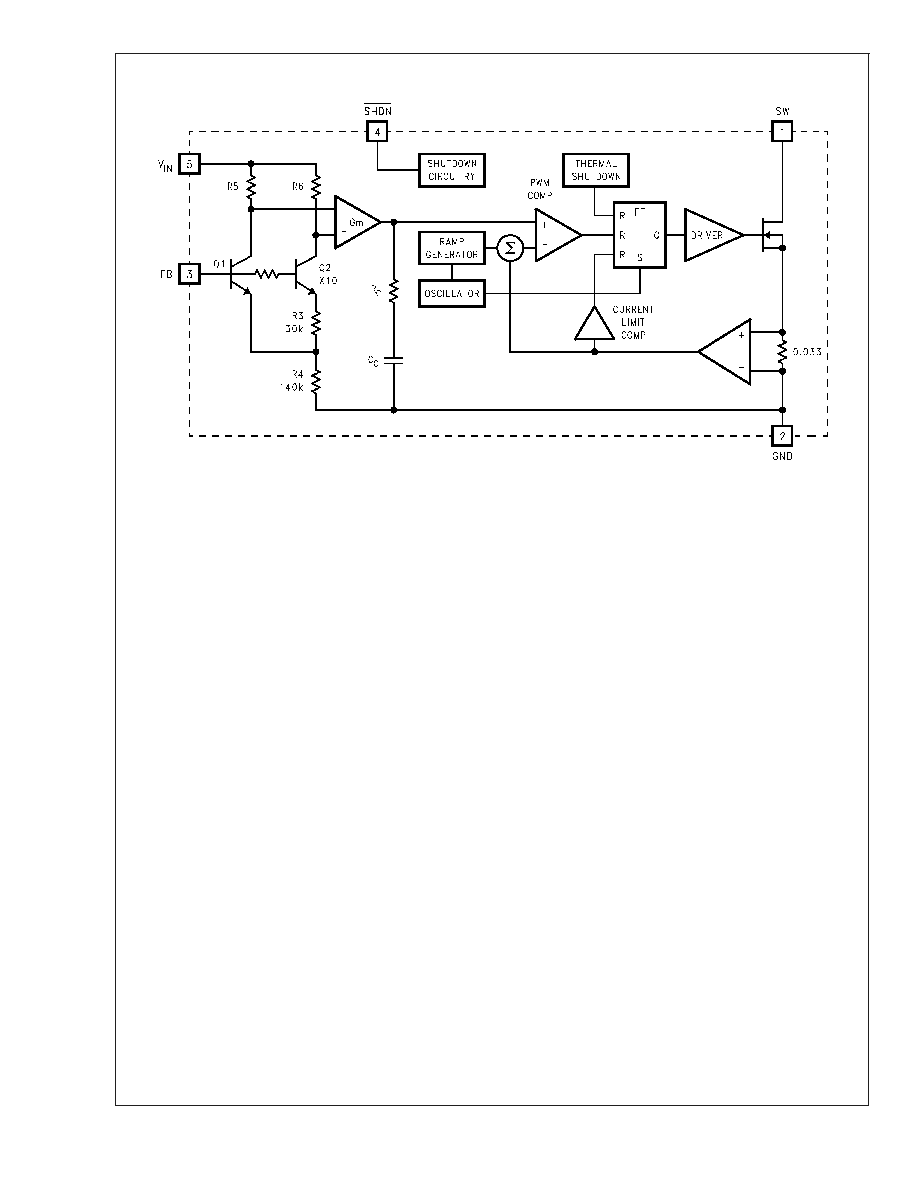
Block Diagram
20059112
Theory of Operation
The LM2731 is a switching converter IC that operates at a
fixed frequency (0.6 or 1.6 MHz) for fast transient response
over a wide input voltage range and incorporates pulse-by-
pulse current limiting protection. Because this is current
mode control, a 33 m
sense resistor in series with the
switch FET is used to provide a voltage (which is propor-
tional to the FET current) to both the input of the pulse width
modulation (PWM) comparator and the current limit ampli-
fier.
At the beginning of each cycle, the S-R latch turns on the
FET. As the current through the FET increases, a voltage
(proportional to this current) is summed with the ramp com-
ing from the ramp generator and then fed into the input of the
PWM comparator. When this voltage exceeds the voltage on
the other input (coming from the Gm amplifier), the latch
resets and turns the FET off. Since the signal coming from
the Gm amplifier is derived from the feedback (which
samples the voltage at the output), the action of the PWM
comparator constantly sets the correct peak current through
the FET to keep the output voltage in regulation.
Q1 and Q2 along with R3 - R6 form a bandgap voltage
reference used by the IC to hold the output in regulation. The
currents flowing through Q1 and Q2 will be equal, and the
feedback loop will adjust the regulated output to maintain
this. Because of this, the regulated output is always main-
tained at a voltage level equal to the voltage at the FB node
"multiplied up" by the ratio of the output resistive divider.
The current limit comparator feeds directly into the flip-flop
that drives the switch FET. If the FET current reaches the
limit threshold, the FET is turned off and the cycle terminated
until the next clock pulse. The current limit input terminates
the pulse regardless of the status of the output of the PWM
comparator.
LM2731
www.national.com
4
Absolute Maximum Ratings
(Note 1)
If Military/Aerospace specified devices are required,
please contact the National Semiconductor Sales Office/
Distributors for availability and specifications.
Storage Temperature Range
-65∞C to +150∞C
Operating Junction
Temperature Range
-40∞C to +125∞C
Lead Temp. (Soldering, 5 sec.)
300∞C
Power Dissipation (Note 2)
Internally Limited
FB Pin Voltage
-0.4V to +6V
SW Pin Voltage
-0.4V to +22V
Input Supply Voltage
-0.4V to +14.5V
Shutdown Input Voltage
(Survival)
-0.4V to +14.5V
J-A
(SOT23-5)
265∞C/W
ESD Rating (Note 3)
Human Body Model
2 kV
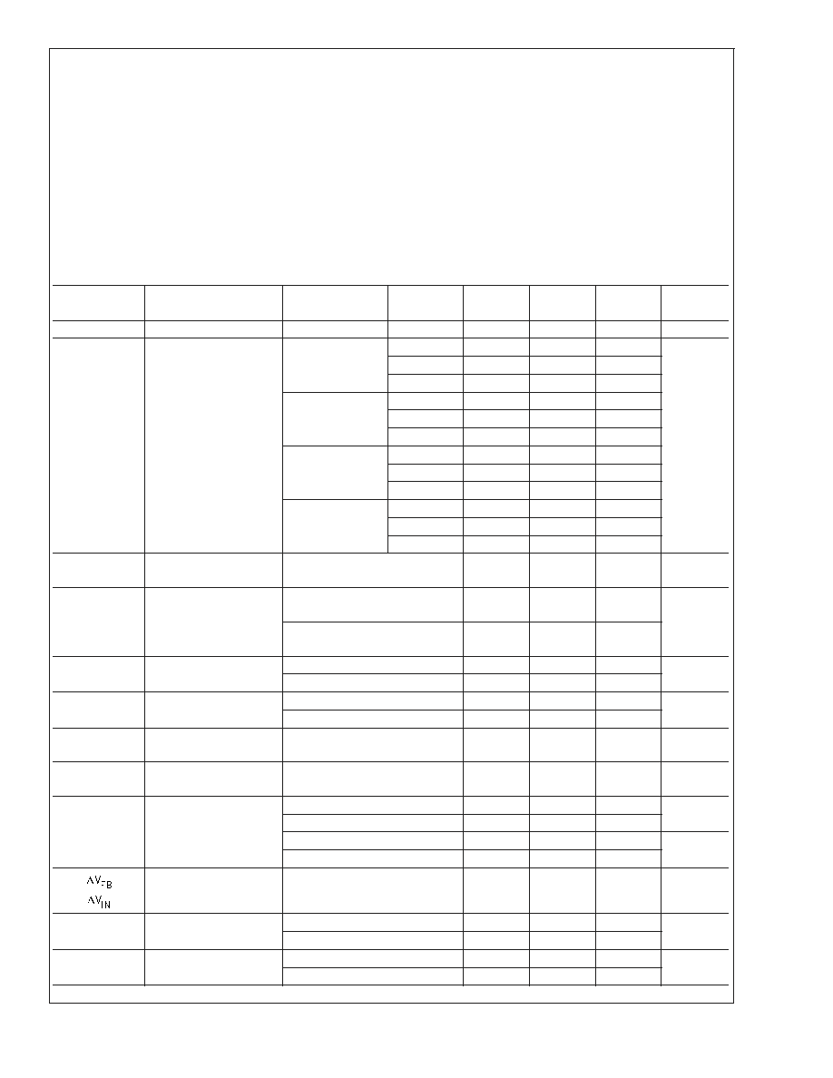
Electrical Characteristics
Limits in standard typeface are for T
J
= 25∞C, and limits in boldface type apply over the full operating temperature range
(-40∞C
T
J
+125∞C). Unless otherwise specified: V
IN
= 5V, V
SHDN
= 5V, I
L
= 0A.
Symbol
Parameter
Conditions
Min
(Note 4)
Typical
(Note 5)
Max
(Note 4)
Units
V
IN
Input Voltage
2.7
14
V
V
OUT (MIN)
Minimum Output Voltage
Under Load
R
L
= 43
X Option
(Note 8)
V
IN
= 2.7V
5.4
7
V
V
IN
= 3.3V
8
10
V
IN
= 5V
13
17
R
L
= 43
Y Option
(Note 8)
V
IN
= 2.7V
8.25
10
V
IN
= 3.3V
10.5
12
V
IN
= 5V
14
16
R
L
= 15
X Option
(Note 8)
V
IN
= 2.7V
3.75
5
V
IN
= 3.3V
5
6.5
V
IN
= 5V
8.75
11
R
L
= 15
Y Option
(Note 8)
V
IN
= 2.7V
5
6
V
IN
= 3.3V
5.5
7.5
V
IN
= 5V
9
11
I
SW
Switch Current Limit
(Note 6)
1.8
1.4
2
A
R
DS
(ON)
Switch ON Resistance
I
SW
= 100 mA
Vin = 5V
260
400
500
m
I
SW
= 100 mA
Vin = 3.3V
300
450
550
SHDN
TH
Shutdown Threshold
Device ON
1.5
V
Device OFF
0.50
I
SHDN
Shutdown Pin Bias
Current
V
SHDN
= 0
0
µA
V
SHDN
= 5V
0
2
V
FB
Feedback Pin Reference
Voltage
V
IN
= 3V
1.205
1.230
1.255
V
I
FB
Feedback Pin Bias
Current
V
FB
= 1.23V
60
500
nA
I
Q
Quiescent Current
V
SHDN
= 5V, Switching "X"
2
3.0
mA
V
SHDN
= 5V, Switching "Y"
1.0
2
V
SHDN
= 5V, Not Switching
400
500
µA
V
SHDN
= 0
0.024
1
FB Voltage Line
Regulation
2.7V
V
IN
14V
0.02
%/V
F
SW
Switching Frequency
(Note 7)
"X" Option
1
1.6
1.85
MHz
"Y" Option
0.40
0.60
0.8
D
MAX
Maximum Duty Cycle
(Note 7)
"X" Option
86
93
%
"Y" Option
92
96
LM2731
www.national.com
5