LM2734Z
Thin SOT23 1A Load Step-Down DC-DC Regulator
General Description
The LM2734Z regulator is a monolithic, high frequency,
PWM step-down DC/DC converter assembled in a 6-pin Thin
SOT23 and LLP non pull back package. It provides all the
active functions to provide local DC/DC conversion with fast
transient response and accurate regulation in the smallest
possible PCB area.
With a minimum of external components and online design
support through WEBENCH
�
TM
, the LM2734Z is easy to
use. The ability to drive 1A loads with an internal 300m
NMOS switch using state-of-the-art 0.5�m BiCMOS technol-
ogy results in the best power density available. The world
class control circuitry allows for on-times as low as 13ns,
thus supporting exceptionally high frequency conversion
over the entire 3V to 20V input operating range down to the
minimum output voltage of 0.8V. Switching frequency is
internally set to 3MHz, allowing the use of extremely small
surface mount inductors and chip capacitors. Even though
the operating frequency is very high, efficiencies up to 85%
are easy to achieve. External shutdown is included, featuring
an ultra-low stand-by current of 30nA. The LM2734Z utilizes
current-mode control and internal compensation to provide
high-performance regulation over a wide range of operating
conditions. Additional features include internal soft-start cir-
cuitry to reduce inrush current, pulse-by-pulse current limit,
thermal shutdown, and output over-voltage protection.
Features
n
Thin SOT23-6 package, or 6 lead LLP package
n
3.0V to 20V input voltage range
n
0.8V to 18V output voltage range
n
1A output current
n
3MHz switching frequency
n
300m
NMOS switch
n
30nA shutdown current
n
0.8V, 2% internal voltage reference
n
Internal soft-start
n
Current-Mode, PWM operation
n
Thermal shutdown
Applications
n
DSL Modems
n
Local Point of Load Regulation
n
Battery Powered Devices
n
USB Powered Devices
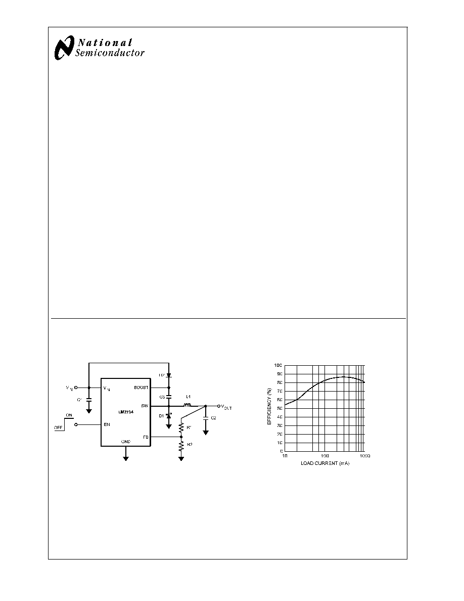
Typical Application Circuit
Efficiency vs Load Current
V
IN
= 5V, V
OUT
= 3.3V
20130301
20130345
WEBENCH
TM
is a trademark of Transim.
March 2005
LM2734Z
Thin
SOT23
1A
Load
Step-Down
DC-DC
Regulator
� 2005 National Semiconductor Corporation
DS201303
www.national.com
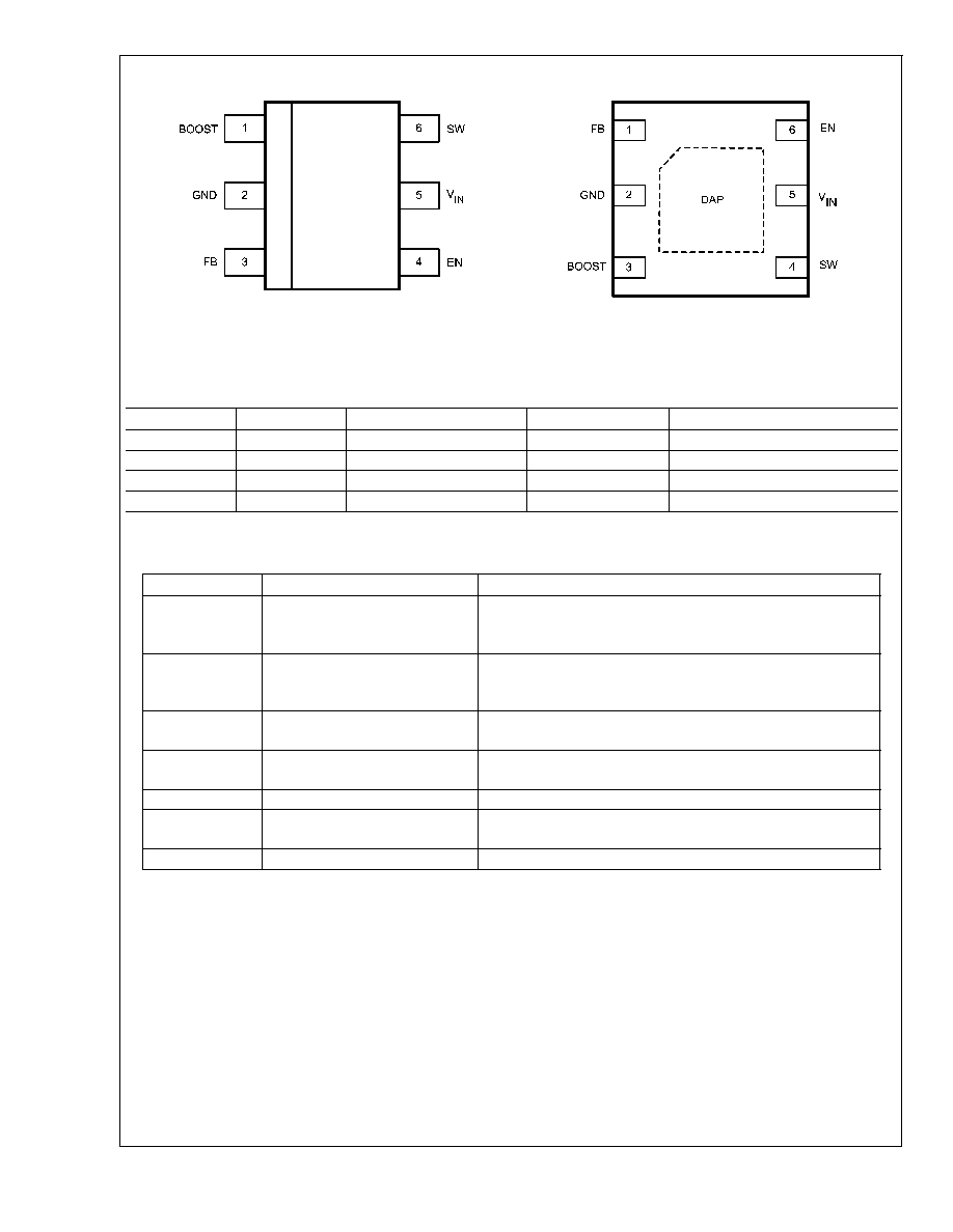
Connection Diagrams
20130305
6-Lead TSOT
NS Package Number MK06A
20130360
6-Lead LLP (3mm x 3mm)
NS Package Number SDE06A
Ordering Information
Order Number
Package Type
NSC Package Drawing
Package Marking
Supplied As
LM2734ZMK
TSOT-6
MK06A
SFTB
1000 Units on Tape and Reel
LM2734ZMKX
TSOT-6
MK06A
SFTB
3000 Units on Tape and Reel
LM2734ZSD
6-Lead LLP
SDE06A
L163B
1000 Units on Tape and Reel
LM2734ZSDX
6-Lead LLP
SDE06A
L163B
4500 Units on Tape and Reel
* Contact the local sales office for the lead-free package.
Pin Description
Pin
Name
Function
1
BOOST
Boost voltage that drives the internal NMOS control switch. A
bootstrap capacitor is connected between the BOOST and SW
pins.
2
GND
Signal and Power ground pin. Place the bottom resistor of the
feedback network as close as possible to this pin for accurate
regulation.
3
FB
Feedback pin. Connect FB to the external resistor divider to set
output voltage.
4
EN
Enable control input. Logic high enables operation. Do not allow
this pin to float or be greater than V
IN
+ 0.3V.
5
V
IN
Input supply voltage. Connect a bypass capacitor to this pin.
6
SW
Output switch. Connects to the inductor, catch diode, and
bootstrap capacitor.
DAP
GND
The Die Attach Pad is internally connected to GND
LM2734Z
www.national.com
2
Absolute Maximum Ratings
(Note 1)
If Military/Aerospace specified devices are required,
please contact the National Semiconductor Sales Office/
Distributors for availability and specifications.
V
IN
-0.5V to 24V
SW Voltage
-0.5V to 24V
Boost Voltage
-0.5V to 30V
Boost to SW Voltage
-0.5V to 6.0V
FB Voltage
-0.5V to 3.0V
EN Voltage
-0.5V to (V
IN
+ 0.3V)
Junction Temperature
150�C
ESD Susceptibility (Note 2)
2kV
Storage Temp. Range
-65�C to 150�C
Soldering Information
Infrared/Convection Reflow (15sec)
220�C
Wave Soldering Lead Temp. (10sec)
260�C
Operating Ratings
(Note 1)
V
IN
3V to 20V
SW Voltage
-0.5V to 20V
Boost Voltage
-0.5V to 25V
Boost to SW Voltage
1.6V to 5.5V
Junction Temperature Range
-40�C to +125�C
Thermal Resistance
JA
(Note 3)
TSOT23�6
118�C/W
Electrical Characteristics
Specifications with standard typeface are for T
J
= 25�C, and those in boldface type apply over the full Operating Tempera-
ture Range (T
J
= -40�C to 125�C). V
IN
= 5V, V
BOOST
- V
SW
= 5V unless otherwise specified. Datasheet min/max specification
limits are guaranteed by design, test, or statistical analysis.
Symbol
Parameter
Conditions
Min
(Note 4)
Typ
(Note 5)
Max
(Note 4)
Units
V
FB
Feedback Voltage
0.784
0.800
0.816
V
V
FB
/
V
IN
Feedback Voltage Line
Regulation
V
IN
= 3V to 20V
0.01
% / V
I
FB
Feedback Input Bias Current
Sink/Source
10
250
nA
UVLO
Undervoltage Lockout
V
IN
Rising
2.74
2.90
V
Undervoltage Lockout
V
IN
Falling
2.0
2.3
UVLO Hysteresis
0.30
0.44
0.62
F
SW
Switching Frequency
2.2
3.0
3.6
MHz
D
MAX
Maximum Duty Cycle
78
85
%
D
MIN
Minimum Duty Cycle
8
%
R
DS(ON)
Switch ON Resistance
V
BOOST
- V
SW
= 3V
(TSOT Package)
300
600
m
V
BOOST
- V
SW
= 3V
(LLP Package)
340
650
m
I
CL
Switch Current Limit
V
BOOST
- V
SW
= 3V
1.2
1.7
2.5
A
I
Q
Quiescent Current
Switching
1.5
2.5
mA
Quiescent Current (shutdown)
V
EN
= 0V
30
nA
I
BOOST
Boost Pin Current
(Switching)
4.25
6
mA
V
EN_TH
Shutdown Threshold Voltage
V
EN
Falling
0.4
V
Enable Threshold Voltage
V
EN
Rising
1.8
I
EN
Enable Pin Current
Sink/Source
10
nA
I
SW
Switch Leakage
40
nA
Note 1: Absolute Maximum Ratings indicate limits beyond which damage to the device may occur. Operating Ratings indicate conditions for which the device is
intended to be functional, but specific performance is not guaranteed. For guaranteed specifications and the test conditions, see Electrical Characteristics.
Note 2: Human body model, 1.5k
in series with 100pF.
Note 3: Thermal shutdown will occur if the junction temperature exceeds 165�C. The maximum power dissipation is a function of T
J(MAX)
,
JA
and T
A
. The
maximum allowable power dissipation at any ambient temperature is P
D
= (T
J(MAX)
� T
A
)/
JA
. All numbers apply for packages soldered directly onto a 3" x 3" PC
board with 2oz. copper on 4 layers in still air. For a 2 layer board using 1 oz. copper in still air,
JA
= 204�C/W.
Note 4: Guaranteed to National's Average Outgoing Quality Level (AOQL).
Note 5: Typicals represent the most likely parametric norm.
LM2734Z
www.national.com
3

Typical Performance Characteristics
All curves taken at V
IN
= 5V, V
BOOST
- V
SW
= 5V, L1 = 2.2 �H
and T
A
= 25�C, unless specified otherwise.
Efficiency vs Load Current
V
OUT
= 5V
Efficiency vs Load Current
V
OUT
= 3.3V
20130336
20130351
Efficiency vs Load Current
V
OUT
= 1.5V
Oscillator Frequency vs Temperature
20130337
20130327
Line Regulation
V
OUT
= 1.5V, I
OUT
= 500mA
Line Regulation
V
OUT
= 3.3V, I
OUT
= 500mA
20130354
20130355
LM2734Z
www.national.com
4
Application Information
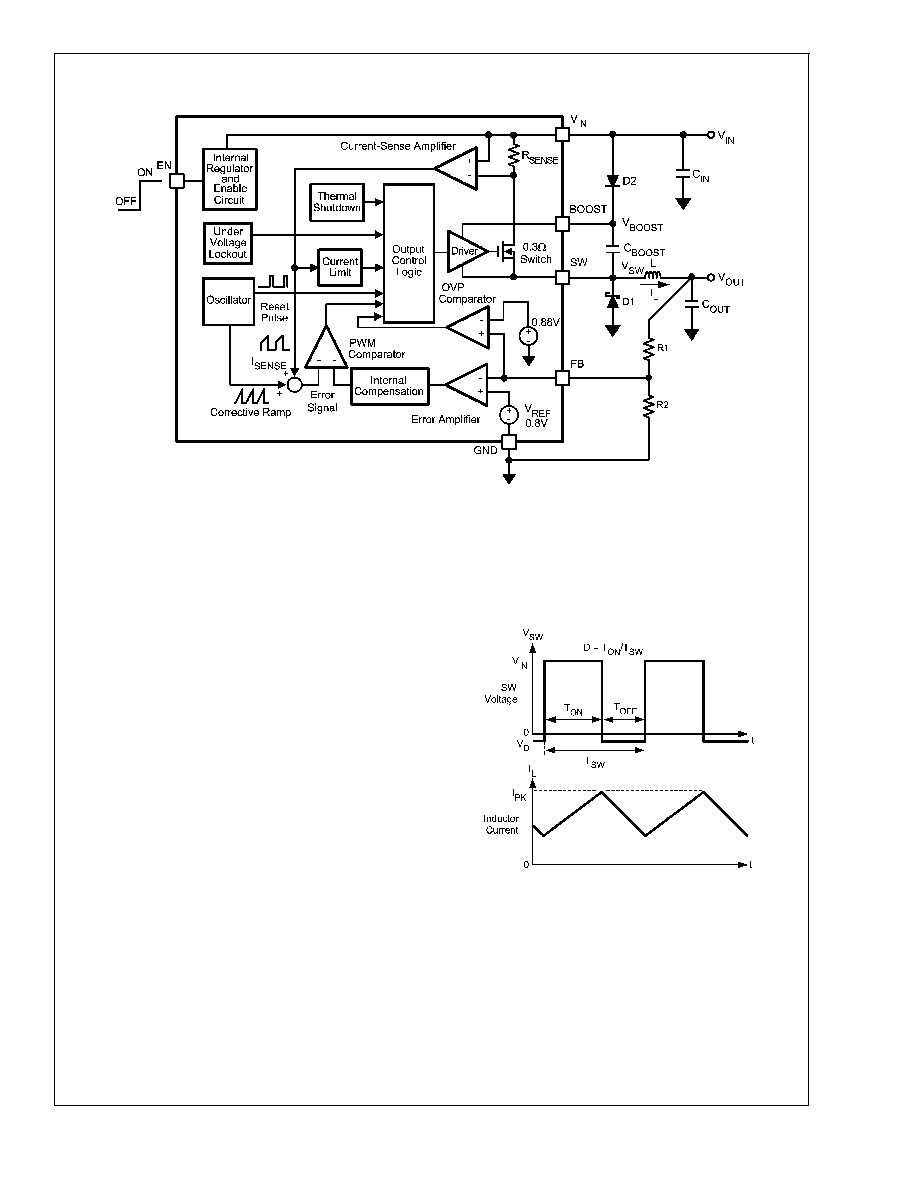
THEORY OF OPERATION
The LM2734Z is a constant frequency PWM buck regulator
IC that delivers a 1A load current. The regulator has a preset
switching frequency of 3MHz. This high frequency allows the
LM2734Z to operate with small surface mount capacitors
and inductors, resulting in a DC/DC converter that requires a
minimum amount of board space. The LM2734Z is internally
compensated, so it is simple to use, and requires few exter-
nal components. The LM2734Z uses current-mode control to
regulate the output voltage.
The following operating description of the LM2734Z will refer
to the Simplified Block Diagram (Figure 1) and to the wave-
forms in Figure 2. The LM2734Z supplies a regulated output
voltage by switching the internal NMOS control switch at
constant frequency and variable duty cycle. A switching
cycle begins at the falling edge of the reset pulse generated
by the internal oscillator. When this pulse goes low, the
output control logic turns on the internal NMOS control
switch. During this on-time, the SW pin voltage (V
SW
) swings
up to approximately V
IN
, and the inductor current (I
L
) in-
creases with a linear slope. I
L
is measured by the current-
sense amplifier, which generates an output proportional to
the switch current. The sense signal is summed with the
regulator's corrective ramp and compared to the error am-
plifier's output, which is proportional to the difference be-
tween the feedback voltage and V
REF
. When the PWM
comparator output goes high, the output switch turns off until
the next switching cycle begins. During the switch off-time,
inductor current discharges through Schottky diode D1,
which forces the SW pin to swing below ground by the
forward voltage (V
D
) of the catch diode. The regulator loop
adjusts the duty cycle (D) to maintain a constant output
voltage.
BOOST FUNCTION
Capacitor C
BOOST
and diode D2 in Figure 3 are used to
generate a voltage V
BOOST
. V
BOOST
- V
SW
is the gate drive
voltage to the internal NMOS control switch. To properly
drive the internal NMOS switch during its on-time, V
BOOST
needs to be at least 1.6V greater than V
SW
. Although the
LM2734Z will operate with this minimum voltage, it may not
have sufficient gate drive to supply large values of output
Block Diagram
20130306
FIGURE 1.
20130307
FIGURE 2. LM2734Z Waveforms of SW Pin Voltage and
Inductor Current
LM2734Z
www.national.com
5