LM2750
Low Noise Switched Capacitor Boost Regulator
General Description
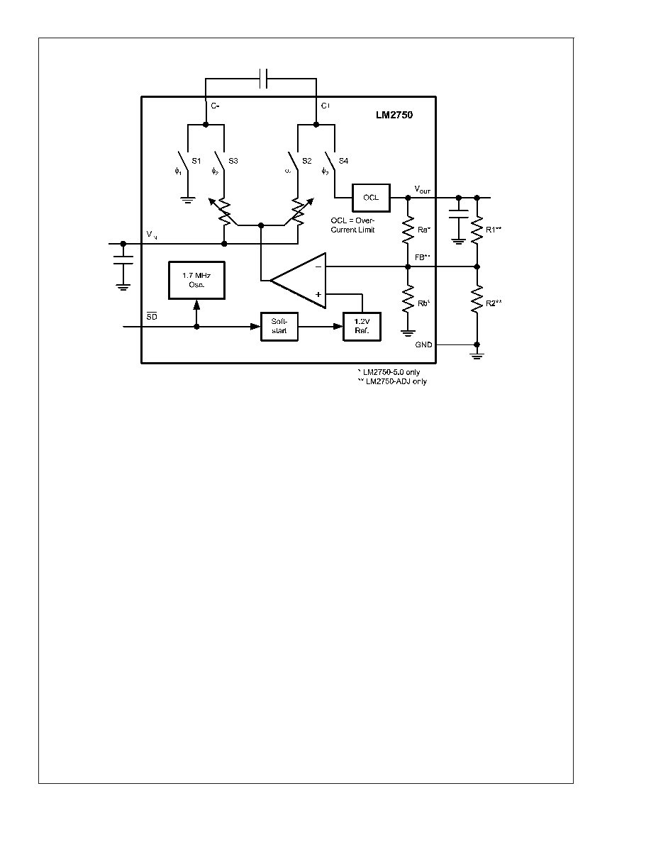
The LM2750 is a regulated switched-capacitor doubler that
produces a low-noise output voltage. The 5.0V output volt-
age option (LM2750-5.0) can supply up to 120mA of output
current over a 2.9V to 5.6V input range, as well as up to
40mA of output current when the input voltage is as low as
2.7V. An adjustable output voltage option with similar output
current capabilities is also available (LM2750-ADJ). The
LM2750 has been placed in National's 10-pin LLP, a pack-
age with excellent thermal properties that keeps the part
from overheating under almost all rated operating conditions
A perfect fit for space-constrained, battery-powered applica-
tions, the LM2750 requires only 3 external components: one
input capacitor, one output capacitor, and one flying capaci-
tor. Small, inexpensive ceramic capacitors are recom-
mended for use. These capacitors, in conjunction with the
1.7MHz fixed switching frequency of the LM2750, yield low
output voltage ripple, beneficial for systems requiring a low-
noise supply. Pre-regulation minimizes input current ripple,
reducing input noise to negligible levels.
A tightly controlled soft-start feature limits inrush currents
during part activation. Shutdown completely disconnects the
load from the input. Output current limiting and thermal
shutdown circuitry protect both the LM2750 and connected
devices in the event of output shorts or excessive current
loads.
Features
n
Inductorless solution: Application requires only 3 small
ceramic capacitors
n
Fixed 5.0V output and adjustable output voltage options
available
n
85% Peak Efficiency
70% Average Efficiency over Li-Ion Input Range
(2.9V-to-4.2V)
n
Output Current up to 120mA with 2.9V
V
IN
5.6V
Output Current up to 40mA with 2.7V
V
IN
2.9V
n
Wide Input Voltage Range: 2.7V to 5.6V
n
Fixed 1.7MHz switching frequency for a low-noise,
low-ripple output signal
n
Pre-regulation minimizes input current ripple, keeping
the battery line (V
IN
) virtually noise-free
n
Tiny LLP package with outstanding power dissipation:
Usually no derating required.
n
Shutdown Supply Current less than 2µA
Applications
n
White and Colored LED-based Display Lighting
n
Cellular Phone SIM cards
n
Audio Amplifier Power Supplies
n
General Purpose Li-Ion-to-5V Conversion
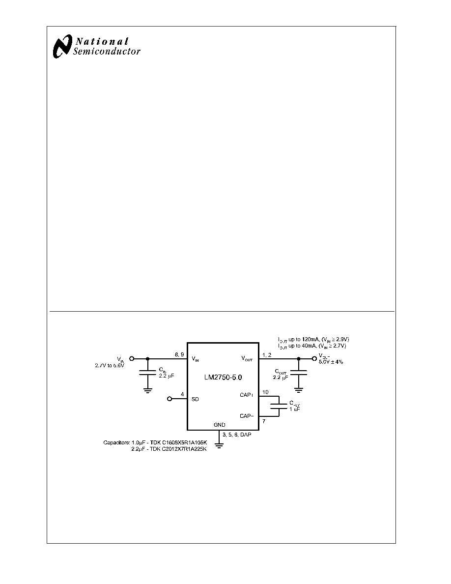
Typical Application Circuit
20035101
July 2004
LM2750
Low
Noise
Switched
Capacitor
Boost
Regulator
© 2004 National Semiconductor Corporation
DS200351
www.national.com
Connection Diagram
LM2750
10-Pin Leadless Leadframe Package (LLP) - 3mm X 3mm
NS Package Number LDA10A
20035102
Top View
Pin Description
Pin #(s)
Pin Name
Description
8, 9
V
IN
Input Voltage - The pins must be connected externally.
1, 2
V
OUT
Output Voltage - These pins must be connected externally.
10
CAP+
Flying Capacitor Positive Terminal
7
CAP-
Flying Capacitor Negative Terminal
4
SD
Active-Low Shutdown Input. A 200k
resistor is connected internally between
this pin and GND to pull the voltage on this pin to 0V, and shut down the part,
when the pin is left floating.
3
LM2750-5.0: GND
This pin must be connected exernally to the ground pins (pins 5, 6, and the
DAP).
LM2750-ADJ: FB
Feedback Pin
5, 6, DAP
GND
Ground - These pins must be connected externally.
Ordering Information
Output Voltage
Option
Ordering
Information
Package Marking
Supplied as
5.0
LM2750LD-5.0
S002B
1000 Units, Tape and Reel
5.0
LM2750LDX-5.0
S002B
4500 Units, Tape and Reel
Adjustable
LM2750LD-ADJ
S003B
1000 Units, Tape and Reel
Adjustable
LM2750LDX-ADJ
S003B
4500 Units, Tape and Reel
LM2750
www.national.com
2
Absolute Maximum Ratings
(Notes 1, 2)
If Military/Aerospace specified devices are required,
please contact the National Semiconductor Sales Office/
Distributors for availability and specifications.
V
IN
Pin: Voltage to Ground
-0.3V to 6V
SD Pin: Voltage to GND
-0.3V to
(V
IN
+0.3V)
Junction Temperature (T
J-MAX-ABS
)
150°C
Continuous Power Dissipation
Internally Limited
(Note 3)
Storage Temperature Range
-65°C to 150°C
Maximum Lead Temperature
260°C
(Soldering, 5 sec.)
ESD Rating (Note 4)
Human-body model:
Machine model
2 kV
100V
Operating Ratings
(Notes 1, 2)
LM2750-5.0 Input Voltage Range
2.7V to 5.6V
LM2750-ADJ Input Voltage Range
3.8V
V
OUT
4.9V:
2.7V to (V
OUT
+0.7V)
4.9V
V
OUT
5.2V:
2.7V to 5.6V
LM2750-ADJ Output Voltage Range
3.8V to 5.2V
Recommended Output Current
2.9V
V
IN
5.6V
0 to 120mA
2.7V
V
IN
2.9V
0 to 40mA
Junction Temperature (T
J
) Range
-40°C to 125°C
Ambient Temperature (T
A
) Range
-40°C to 85°C
(Note 5)
Thermal Information
Junction-to-Ambient Thermal
Resistance, LLP-10
55°C/W
Package (
JA
) (Note 6)
Electrical Characteristics
(Notes 2, 7)
Typical values and limits in standard typeface apply for T
J
= 25
o
C. Limits in boldface type apply over the operating junction
temperature range. Unless otherwise specified: 2.9V
V
IN
5.6V, V
OUT
= 5.0V (LM2750-ADJ), V(SD) = V
IN
, C
FLY
= 1µF, C
IN
= 2 x 1µF, C
OUT
= 2 x 1µF (Note 8).
Symbol
Parameter
Conditions
Min
Typ
Max
Units
V
OUT
Output Voltage
(LM2750-5.0)
2.9V
V
IN
5.6V,
I
OUT
120mA
4.80
(-4%)
5.0
5.20
(+4%)
V
(%)
2.7V
V
IN
2.9V,
I
OUT
40mA
4.80
(-4%)
5.0
5.20
(+4%)
I
Q
Operating Supply Current
I
OUT
= 0mA,
V
IH(MIN)
V(SD) V
IN
5
10
12
mA
I
SD
Shutdown Supply Current
V(SD) = 0V
2
µA
V
FB
Feedback Pin Voltage
(LM2750-ADJ)
V
IN
= 3.1V
1.170
1.232
1.294
V
I
FB
Feedback Pin Input Current
(LM2750-ADJ)
V
FB
= 1.4V
1
nA
V
R
Output Ripple
C
OUT
= 10µF, I
OUT
= 100mA
4
mVp-p
C
OUT
= 2.2µF, I
OUT
= 100mA
15
E
PEAK
Peak Efficiency
(LM2750-5.0)
V
IN
= 2.7V, I
OUT
= 40mA
87
%
V
IN
= 2.9V, I
OUT
= 120mA
85
E
AVG
Average Efficiency over Li-Ion
Input Range
(LM2750-5.0)
(Note 10)
V
IN
Range: 2.9V - 4.2V,
I
OUT
= 120mA
70
%
V
IN
Range: 2.9V - 4.2V,
I
OUT
= 40mA
67
f
SW
Switching Frequency
1.0
1.7
MHz
t
ON
V
OUT
Turn-On Time
V
IN
= 3.0V, I
OUT
= 100mA,
(Note 9)
0.5
ms
I
LIM
Current Limit
V
OUT
shorted to GND
300
mA
Shutdown Pin (SD) Characteristics
V
IH
Logic-High SD Input
1.3
V
IN
V
V
IL
Logic-Low SD Input
0
0.4
V
I
IH
SD Input Current (Note 11)
1.3V
V(SD) V
IN
15
50
µA
I
IL
SD Input Current
V(SD) = 0V
-1
1
µA
LM2750
www.national.com
3
Electrical Characteristics
(Notes 2, 7) (Continued)
Typical values and limits in standard typeface apply for T
J
= 25
o
C. Limits in boldface type apply over the operating junction
temperature range. Unless otherwise specified: 2.9V
V
IN
5.6V, V
OUT
= 5.0V (LM2750-ADJ), V(SD) = V
IN
, C
FLY
= 1µF, C
IN
= 2 x 1µF, C
OUT
= 2 x 1µF (Note 8).
Symbol
Parameter
Conditions
Min
Typ
Max
Units
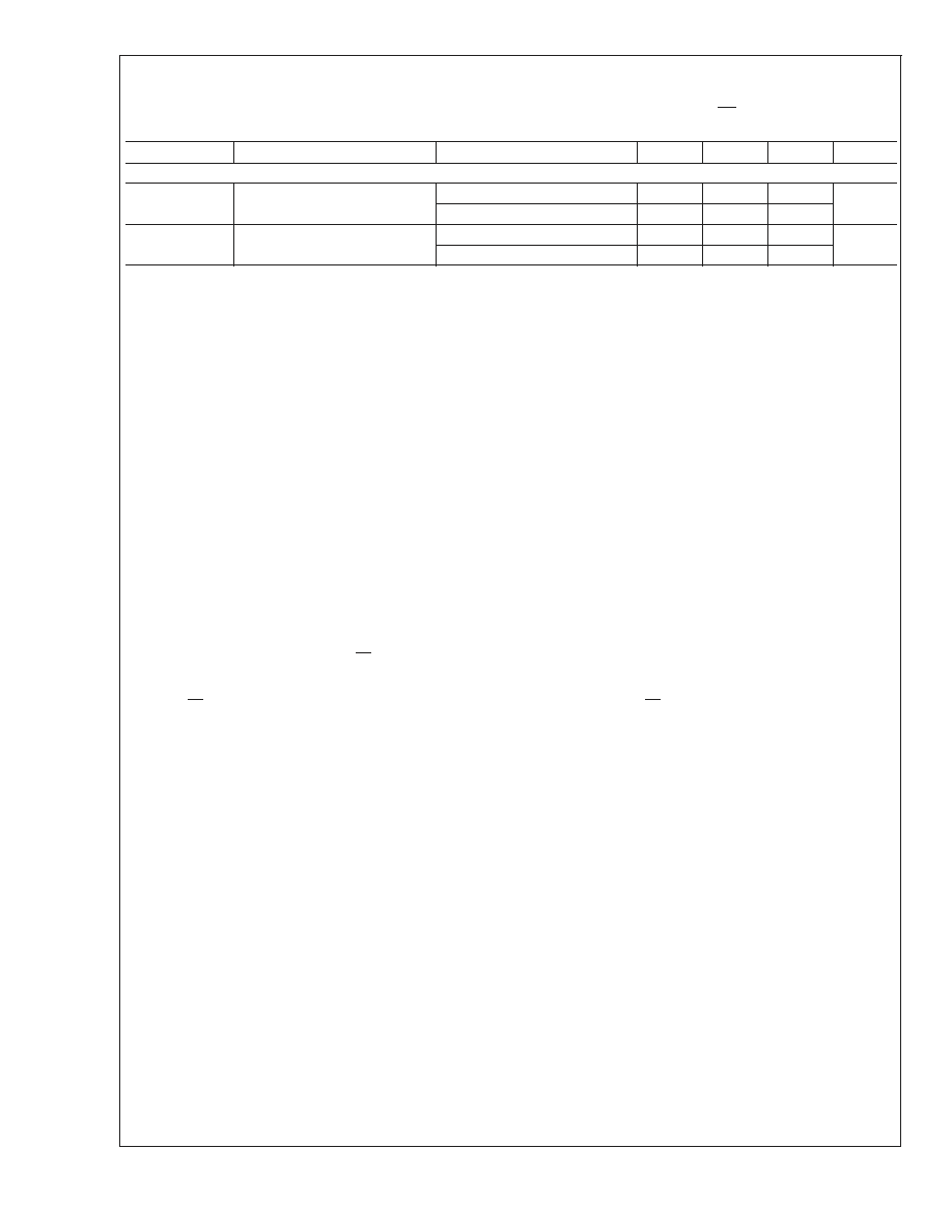
Capacitor Requirements
C
IN
Required Input
Capacitance(Note 12)
I
OUT
60mA
1.0
µF
60mA
I
OUT
120mA
2.0
C
OUT
Required Output
Capacitance(Note 12)
I
OUT
60mA
1.0
µF
60mA
I
OUT
120mA
2.0
Note 1: Absolute Maximum Ratings indicate limits beyond which damage to the component may occur. Operating Ratings are conditions under which operation of
the device is guaranteed. Operating Ratings do not imply guaranteed performance limits. For guaranteed performance limits and associated test conditions, see the
Electrical Characteristics tables.
Note 2: All voltages are with respect to the potential at the GND pin.
Note 3: Thermal shutdown circuitry protects the device from permanent damage. Thermal shutdown engages at T
J
=150°C (typ.) and disengages at T
J
=135°C (typ.).
Note 4: The Human body model is a 100 pF capacitor discharged through a 1.5 k
resistor into each pin. MIL-STD-883 3015.7. The machine model is a 200pF
capacitor discharged directly into each pin.
Note 5: Maximum ambient temperature (T
A-MAX
) is dependent on the maximum operating junction temperature (T
J-MAX-OP
= 125
o
C), the maximum power
dissipation of the device in the application (P
D-MAX
), and the junction-to ambient thermal resistance of the part/package in the application (
JA
), as given by the
following equation: T
A-MAX
= T
J-MAX-OP
- (
JA
x P
D-MAX
). Maximum power dissipation of the LM2750 in a given application can be approximated using the following
equation: P
D-MAX
= (V
IN-MAX
x I
IN-MAX
) - (V
OUT
x I
OUT-MAX
) = [V
IN-MAX
x ((2 x I
OUT-MAX
) + 5mA)] - (V
OUT
x I
OUT-MAX
). In this equation, V
IN-MAX
, I
IN-MAX
, and
I
OUT-MAX
are the maximum voltage/current of the specific application, and not necessarily the maximum rating of the LM2750.
The maximum ambient temperature rating of 85
o
C is determined under the following application conditions:
JA
= 55
o
C/W, P
D-MAX
= 727mW (achieved when
V
IN-MAX
= 5.5V and I
OUT-MAX
= 115mA, for example). Maximum ambient temperature must be derated by 1.1
o
C for every increase in internal power dissipation of
20mW above 727mW (again assuming that
JA
= 55
o
C/W in the application). For more information on these topics, please refer to Application Note 1187: Leadless
Leadframe Package (LLP) and the Power Efficiency and Power Dissipation section of this datasheet.
Note 6: Junction-to-ambient thermal resistance (
JA
) is taken from a thermal modeling result, performed under the conditions and guidelines set forth in the JEDEC
standard JESD51-7. The test board is a 4 layer FR-4 board measuring 102mm x 76mm x 1.6mm with a 2 x 1 array of thermal vias. The ground plane on the board
is 50mm x 50mm. Thickness of copper layers are 36µm/18µm /18µm/36µm (1.5oz/1oz/1oz/1.5oz). Ambient temperature in simulation is 22°C, still air. Power
dissipation is 1W.
The value of
JA
of the LM2750 in LLP-10 could fall in a range as wide as 50
o
C/W to 150
o
C/W (if not wider), depending on PCB material, layout, and environmental
conditions. In applications where high maximum power dissipation exists (high V
IN
, high I
OUT
), special care must be paid to thermal dissipation issues. For more
information on these topics, please refer to Application Note 1187: Leadless Leadframe Package (LLP) and the Layout Recommendations section of this
datasheet.
Note 7: Min and Max limits are guaranteed by design, test, or statistical analysis. Typical numbers are not guaranteed, but do represent the most likely norm.
Note 8: C
FLY
, C
IN
, and C
OUT
: Low-ESR Surface-Mount Ceramic Capacitors (MLCCs) used in setting electrical characteristics
Note 9: Turn-on time is measured from when SD signal is pulled high until the output voltage crosses 90% of its final value.
Note 10: Efficiency is measured versus V
IN
, with V
IN
being swept in small increments from 3.0V to 4.2V. The average is calculated from these measurements
results. Weighting to account for battery voltage discharge characteristics (V
BAT
vs. Time) is not done in computing the average.
Note 11: SD Input Current (I
IH
) is due to a 200k
(typ.) pull-down resistor connected internally between the SD pin and GND.
Note 12: Limit is the minimum required output capacitance to ensure proper operation. This electrical specification is guaranteed by design.
LM2750
www.national.com
4