LM2751
Regulated 2X, 1.5X Switched Capacitor White LED Driver
General Description
The LM2751 is a constant frequency switched capacitor
charge pump with regulated output voltage options of 4.5V,
and 5.0V. Over the input voltage range of 2.8V to 5.5V the
LM2751 provides up to 150mA of output current and requires
only four low-cost ceramic capacitors.
The LM2751 provides excellent efficiency without the use of
an inductor by operating the charge pump in a gain of 3/2 or
2. The proper gain for maintaining regulation is chosen so
that efficiency is maximized over the input voltage range.
LM2751 uses constant frequency pre-regulation to minimize
conducted noise on the input and provide a predictable
switching frequency. The switching frequency is program-
mable to 725kHz, 300kHz, 37kHz, or 9.5kHz.
LM2751 is available in a 10-pin Leadless Leadframe No-
Pullback Package: LLP-10.
Features
n
Regulated Output Options: 4.5V, 5.0V
n
Output Voltage Regulated within 3%
n
Peak Efficiency Over 90%
n
150mA (4.5V) or 80mA (5.0V) Output Current Capability
n
Input Voltage Range: 2.8V to 5.5V
n
Low Input and Output Voltage Ripple
n
<
1�A Typical Shutdown Current
n
Small Solution Size - NO INDUCTOR
n
Programmable 725kHz, 300kHz, 37kHz, or 9.5kHz
Switching Frequencies
n
10-pin LLP No-Pullback Package: 3mm x 3mm x 0.8mm
Applications
n
White LED Display Backlights
n
White LED Keypad Backlights
n
General Purpose 2x, 1.5x Regulated Charge Pump
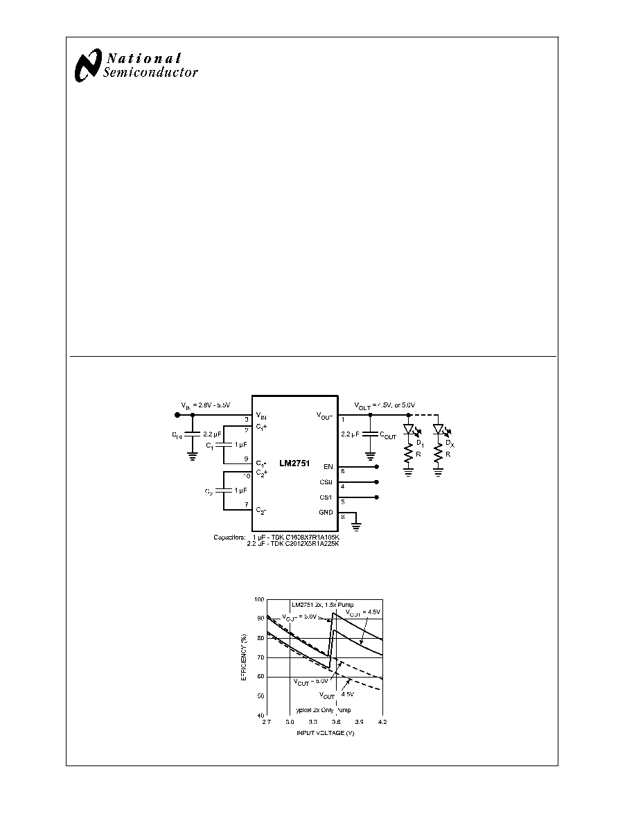
Typical Application Circuit
20112101
LM2751 2x/1.5x Efficiency vs.
2x Charge Pump Effciency
20112128
April 2005
LM2751
Regulated
2X,
1.5X
Switched
Capacitor
White
LED
Driver
� 2005 National Semiconductor Corporation
DS201121
www.national.com
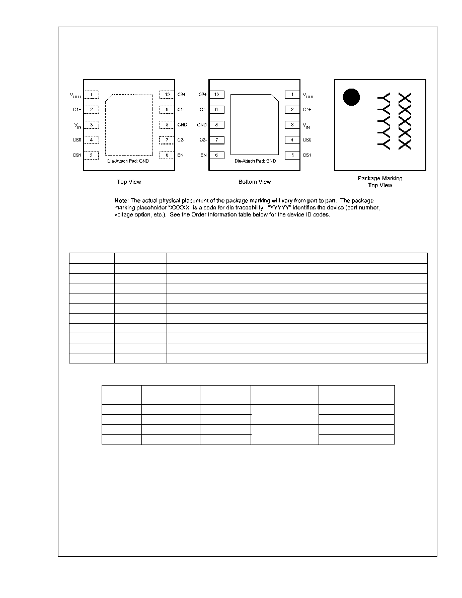
Connection Diagram
10-pin Leadless Leadframe Package (LLP-10) No Pullback
3mm x 3mm x 0.8mm
NS Package Number SDA10A
20112102
Pin Descriptions
Pin #
Name
Description
1
V
OUT
Pre-Regulated Output.
2
C
1+
Flying Capacitor C1 Connection.
3
V
IN
Input Supply Range: 2.8V to 5.5V.
4
CS0
Frequency Select Input 0.
5
CS1
Frequency Select Input 1.
6
EN
Enable Pin Logic Input.
7
C
2-
Flying Capacitor C2 Connection.
8
GND
Ground.
9
C
1-
Flying Capacitor C1 Connection.
10
C
2+
Flying Capacitor C2 Connection.
Ordering Information
Version
Voltage Option
Order Number
Package Marking
Supplied As Tape and
Reel
A
5.0V
LM2751SD-A
XXXXX
YYYYY = L145B
1000 Units
A
5.0V
LM2751SDX-A
4500 Units
B
4.5V
LM2751SD-B
XXXXX
YYYYY = L146B
1000 Units
B
4.5V
LM2751SDX-B
4500 Units
LM2751
www.national.com
2
Absolute Maximum Ratings
(Notes 1, 2)
If Military/Aerospace specified devices are required,
please contact the National Semiconductor Sales Office/
Distributors for availability and specifications.
V
IN
Pin
-0.3V to 6.0V
EN, CS0, CS1 Pins
-0.3V to (V
IN
+0.3)
w/ 6.0V max
Continuous Power Dissipation
(Note 3)
Internally Limited
Junction Temperature
(T
J-MAX-ABS
)
150�C
Storage Temperature Range
-65�C to 150�C
Maximum Lead Temperature
265�C
(Soldering, 10sec.)
ESD Rating (Note 4)
Human-body model:
Machine model:
2kV
200V
Operating Ratings
(Notes 1, 2)
Input Voltage Range
2.8V to 5.5V
EN, CS0, CS1 Input Voltage Range
0V to V
IN
Junction Temperature (T
J
) Range
-40�C to 115�C
Ambient Temperature (T
A
) Range
-40�C to 85�C
(Note 5)
Recommended Maximum Load Current
Version
Freq. = 725kHz
150mA
B
Freq. = 300kHz
120mA
Freq. = 37kHz
40mA
Freq. = 9.5kHz
10mA
Version
Freq. = 725kHz
80mA
A
Freq. = 300kHz
60mA
Freq. = 37kHz
16mA
Freq. = 9.5kHz
4mA
Thermal Properties
Junction-to-Ambient Thermal
Resistance, LLP-10
55�C/W
Package (
JA
) (Note 6)
Electrical Characteristics
(Notes 2, 7)
Limits in standard typeface are for T
A
= 25
o
C. Limits in boldface type apply over the full operating ambient temperature range
(-40�C
T
A
+85�C) . Unless otherwise noted, specifications apply to the LM2751 Typical Application Circuit (pg. 1) with: V
IN
= 3.6V, V(EN) = V
IN,
CS0 = CS1 = V
IN
, C
1
= C
2
= 1.0�F, C
IN
= C
OUT
= 2.2�F (Note 8).
Symbol
Parameter
Conditions
Min
Typ
Max
Units
V
OUT
Output Voltage
Version A, 2.8V
V
IN
5.5V,
Freq. = 300kHz, 725kHz, T
A
= 25�C
I
OUT
= 0 to 60mA
4.850
(-3%)
5.0
5.150
(+3%)
V
Version A, 2.8V
V
IN
5.5V,
Freq. = 300kHz, I
OUT
= 0 to 60mA
Freq. = 725kHz, I
OUT
= 0 to 80mA
4.775
(-4.5%)
5.225
(+4.5%)
Version B, 2.8V
V
IN
5.5V,
Freq. = 300kHz, 725kHz, T
A
= 25�C
I
OUT
= 0 to 120mA
4.343
(-3.5%)
4.5
4.658
(+3.5%)
Version B, 2.8V
V
IN
5.5V,
Freq. = 300kHz, I
OUT
= 0 to 120mA
Freq. = 725kHz, I
OUT
= 0 to 150mA
4.275
(-5%)
4.725
(+5%)
V
R
Output Ripple
2.8V
V
IN
5.5V
I
OUT
= 60mA
8
mV
I
Q
Quiescent Current
Freq. = 9.5kHz, I
OUT
= 0mA, V
IN
= 3.7V
425
600
�A
Freq. = 37kHz, I
OUT
= 0mA, V
IN
= 3.7V
450
640
Freq. = 300kHz, I
OUT
= 0mA, V
IN
= 3.7V
700
900
Freq. = 725kHz, I
OUT
= 0mA, V
IN
= 3.7V
1000
1500
I
SD
Shutdown Supply Current
V(EN) = 0V
0.77
1.3
�A
V(EN) = 0V, T
A
= 85�C
1.0
E
Efficiency
I
OUT
= 80mA (Version A, 5.0V)
Freq. = 300kHz, 725kHz
92
%
I
OUT
= 150mA (Version B, 4.5V)
Freq. = 300kHz, 725kHz
83
LM2751
www.national.com
3
Electrical Characteristics
(Notes 2, 7) (Continued)
Limits in standard typeface are for T
A
= 25
o
C. Limits in boldface type apply over the full operating ambient temperature range
(-40�C
T
A
+85�C) . Unless otherwise noted, specifications apply to the LM2751 Typical Application Circuit (pg. 1) with: V
IN
= 3.6V, V(EN) = V
IN,
CS0 = CS1 = V
IN
, C
1
= C
2
= 1.0�F, C
IN
= C
OUT
= 2.2�F (Note 8).
Symbol
Parameter
Conditions
Min
Typ
Max
Units
fsw
Switching Frequency
CS0 = High, CS1 = Low
2.8V
V
IN
5.5V
6.7
(-30%)
9.5
12.3
(+30%)
kHz
CS0 = Low, CS1 = Low
2.8V
V
IN
5.5V
26
(-30%)
37
48
(+30%)
CS0 = Low, CS1 = High
2.8V
V
IN
5.5V
210
(-30%)
300
390
(+30%)
CS0 = High, CS1 = High
2.8V
V
IN
5.5V
508
(-30%)
725
942
(+30%)
V
IH
Logic Input High
Input Pins: EN, CS0, CS1
2.8V
V
IN
5.5V
1.00
V
IN
V
V
IL
Logic Input Low
Input Pins: EN, CS0, CS1
2.8V
V
IN
5.5V
0
.30
V
I
IH
Logic Input High Current
Input Pins: CS0, CS1
V(CSx) = 1.8V
10
nA
Input Pin: EN
V(EN) = 1.8V(Note 9)
2
�A
I
IL
Logic Input Low Current
Input Pins: EN, CS0, CS1
V(EN, CSx) = 0V
10
nA
V
G
Gain Transition Voltage
(Version A, B)
1.5X to 2X
3.50
V
2X to 1.5X
3.58
Hysteresis
40
80
150
mV
I
SC
Short Circuit Output
Current
V
OUT
= 0V
250
mA
t
ON
V
OUT
Turn-On Time
(Note 10)
300
�s
Note 1: Absolute Maximum Ratings indicate limits beyond which damage to the component may occur. Operating Ratings are conditions under which operation of
the device is guaranteed. Operating Ratings do not imply guaranteed performance limits. For guaranteed performance limits and associated test conditions, see the
Electrical Characteristics tables.
Note 2: All voltages are with respect to the potential at the GND pin.
Note 3: Internal thermal shutdown circuitry protects the device from permanent damage. Thermal shutdown engages at T
J
=150�C (typ.) and disengages at
T
J
=140�C (typ.).
Note 4: The Human body model is a 100 pF capacitor discharged through a 1.5k
resistor into each pin. The machine model is a 200pF capacitor discharged
directly into each pin. MIL-STD-883 3015.7
Note 5: In applications where high power dissipation and/or poor package thermal resistance is present, the maximum ambient temperature may have to be
derated. Maximum ambient temperature (T
A-MAX
) is dependent on the maximum operation junction temperature (T
J-MAX-OP
= 115
o
C), the maximum power
dissipation of the device in the application (P
D-MAX
), and the junction-to ambient thermal resistance of the part/package in the application (
JA
), as given by the
following equation: T
A-MAX
= T
J-MAX-OP
- (
JA
x P
D-MAX
).
Note 6: Junction-to-ambient thermal resistance (
JA
) is taken from a thermal modeling result, performed under the conditions and guidelines set forth in the JEDEC
standard JESD51-7. The test board is a 4 layer FR-4 board measuring 102mm x 76mm x 1.6mm with a 2 x 1 array of thermal vias. The ground plane on the board
is 50mm x 50mm. Thickness of copper layers are 36�m/18�m /18�m/36�m (1.5oz/1oz/1oz/1.5oz). Ambient temperature in simulation is 22
o
C, still air. Power
dissipation is 1W.
The value of
JA
of the LM2751 in LLP-10 could fall in a range as wide as 50
o
C/W to 150
o
C/W (if not wider), depending on PWB material, layout, and environmental
conditions. In applications where high maximum power dissipation exists (high V
IN
, high I
OUT
), special care must be paid to thermal dissipation issues. For more
information on these topics, please refer to Application Note 1187: Leadless Leadframe Package (LLP) and the Power Efficiency and Power Dissipation
section of this datasheet.
Note 7: Min and Max limits are guaranteed by design, test, or statistical analysis. Typical numbers are not guaranteed, but represent the most likely norm.
Note 8: C
IN
, C
OUT
, C
1
, and C
2
: Low-ESR Surface-Mount Ceramic Capacitors (MLCCs) used in setting electrical characteristics.
Note 9: EN Logic Input High Current (I
IH
) is due to a 1M
(typ.) pull-down resistor connected internally between the EN pin and GND.
Note 10: Turn-on time is measured from when the EN signal is pulled high until the output voltage on V
OUT
crosses 90% of its final value.
LM2751
www.national.com
4

Block Diagram
20112103
LM2751
www.national.com
5