 | ÐлекÑÑоннÑй компоненÑ: LM2754SQX | СкаÑаÑÑ:  PDF PDF  ZIP ZIP |
Äîêóìåíòàöèÿ è îïèñàíèÿ www.docs.chipfind.ru
LM2754
800mA Switched Capacitor Flash LED Driver with
Time-Out Protection
General Description
The LM2754 is an integrated low noise, high current
switched capacitor DC/DC converter with four regulated cur-
rent sinks. The device is optimized for driving 1 to 4 high
power white LEDs in parallel with a maximum current of
800mA. Maximum efficiency is achieved over the input volt-
age range by actively selecting the proper gain based on the
LED forward voltage and current requirements.
Two external low power resistors set the desired current for
Torch and Flash modes. The TX pin allows the device to be
forced into Torch mode during a Flash pulse, allowing for
synchronization between the RF power amplifier pulse and
Flash/Torch modes. To protect the device and Flash LEDs,
internal Time-Out circuitry turns off the LM2754 in case of a
faulty prolonged Flash mode. Internal soft-start circuitry lim-
its the amount of inrush current during start-up.
The LM2754 is available in a small 24-pin thermally en-
hanced LLP package.
Features
n
Up to 800mA Output Current
n
Wide Operating Input Voltage Range: 2.8V to 5.5V
n
Drives 1, 2, 3 or 4 LEDs in Parallel
n
Ability to Disable One Current Sink Via the SEL Pin to
Accommodate 3-LED Flash Modules
n
Time-Out Circuitry Limits Flash Duration to 1 Second
n
TX Input Ensures Synchronization with RF Power
Amplifier Pulse
n
Adaptive 1x, 1.5x and 2x Gains for Maximum Efficiency
n
1MHz Constant Frequency Operation
n
Output Current Limit
n
True Shutdown Output Disconnect
n
<
1µA Shutdown Current
n
Internal Soft-Start Limits Inrush Current
n
No Inductor Required
n
Total Solution Size without LED
<
28mm
2
n
Low Profile 24-Pin LLP Package (4mm x 4mm x 0.8mm)
Applications
n
Camera Flash in Mobile Phones
n
Flash for Digital Cameras
n
Supplies for DSP's, Microprocessors, Memory, MP3
Players, Pagers, Other Portable Devices
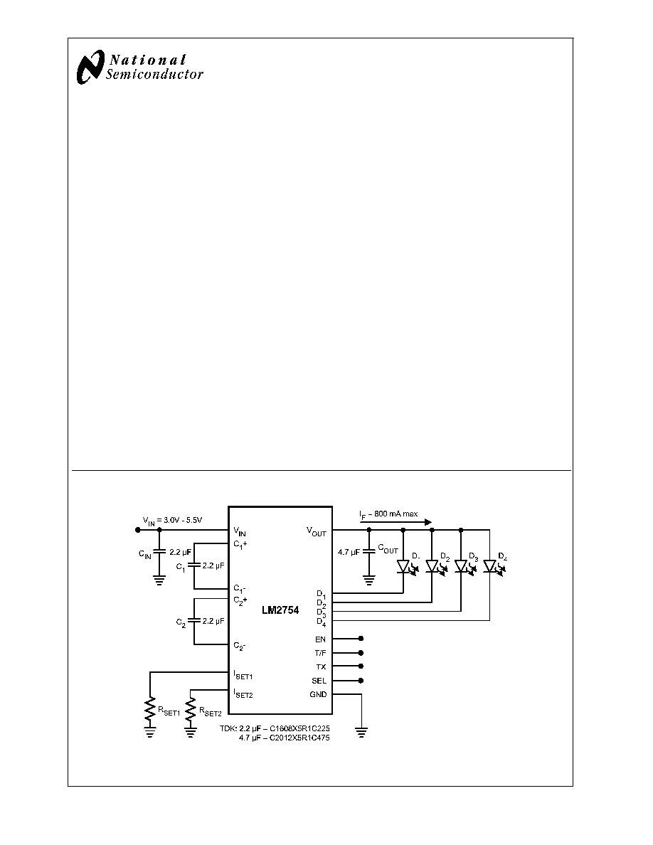
Typical Application Circuit
20202801
September 2006
LM2754
800mA
Switched
Capacitor
Flash
LED
Driver
with
T
ime-Out
Protection
© 2006 National Semiconductor Corporation
DS202028
www.national.com
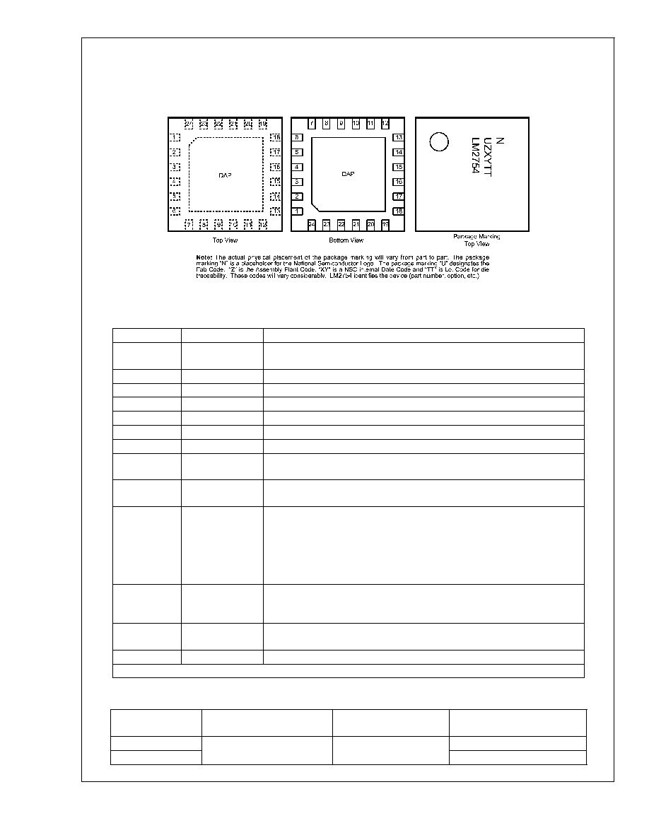
Connection Diagram
LM2754
24-pin No-Pullback Leadless Leadframe Package (LLP-24)
4mm x 4mm x 0.8mm
NS Package Number SQA24A
20202802
Pin Descriptions
Pin
Name
Description
23,24
V
INSW
Input Voltage Connection for Switch Array. Pins 23 and 24 are connected
internally on the die. Connect V
IN
and V
INSW
pins together.
22
V
IN
Input Voltage Connection. Connect V
IN
and V
INSW
pins together.
8
V
OUT
Output Voltage. Connect to LED Anodes.
12, 13, 14, 15
D1, D2, D3, D4*
Regulated Current Sink Inputs. (* See SEL PIN description)
1, 2, 7, 5
C
1
+, C
1
-, C
2
+, C
2
- Flying Capacitor Connections.
3
GND
SW
Switch Array Ground Connection. Connect GND and GND
SW
pins together.
9, 16, 17
GND
Ground Connection. Connect GND and GND
SW
pins together.
21
EN
Enable Control Pin. Logic High = Normal Operation in Torch Mode.
Logic Low = Device Shut-Down. (See Note)
20
T/F
Torch/Flash Control Pin. Logic High = Flash Mode. Logic Low = Torch Mode.
Device must be enabled for Torch or Flash to operate. (See Note)
10, 11
I
SET1
, I
SET2
Current Set Resistor Connections. Connect 1% resistors to ground to set the
desired current through the LEDs. LED current is approximated by the
equation: 800 x (1.25V ÷ R). This equation corresponds to the current through
one current sink. Total LED current is equal to the sum of currents through all
current sinks connected to the LED. The equation used for Torch (I
SET1
) and
Flash (I
SET2
) resistors are the same.
19
TX
RF PA synchronization control pin. Logic High = Force Torch Mode. Logic Low
= Normal Operation. (See Applications Information section for the full
operational description) (See Note)
18
SEL
D
4
Control Pin. Logic Low = Normal 4-LED Operation. Logic High = Disable
D
4
LED Input. Connect D
4
to V
OUT
when not used. (See Note)
4, 6
No Connect
Do not connect to any node.
Note: EN, T/F, TX, and SEL pins each have a 500k
resistor connected internally to GND
Ordering Information
Order Number
Package Description
Package Marking
Supplied as Tape and Reel
(Units)
LM2754SQ
No-Pullback
LLP-24
UZXYTT
LM2754
1000
LM2754SQX
4500
LM2754
www.national.com
2
Absolute Maximum Ratings
(Notes 1, 2)
If Military/Aerospace specified devices are required,
please contact the National Semiconductor Sales Office/
Distributors for availability and specifications.
V
IN
, V
OUT
pins
-0.3V to 6.0V
EN, T/F, TX, SEL pins
-0.3V to (V
IN
+ 0.3V)
w/ 6.0V max
Continuous Power Dissipation
(Note 3)
Internally Limited
Junction Temperature
(T
J-MAX-ABS
)
150°C
Storage Temperature Range
-65°C to 150°C
Lead Temp. (Soldering, 5 sec.)
260°C
ESD Rating (Note 4)
Human Body Model
2kV
Operating Ratings
(Notes 1, 2)
Input Voltage (V
IN
)
2.8V to 5.5V
Junction Temperature Range (T
J
)
-40°C to +125°C
Ambient Temperature Range (T
A
)
(Note 5)
-40°C to +85 °C
Thermal Information
Junction-to-Ambient Thermal Resistance,
LLP-24 Package (
JA
)
(Note 6)
42°C/W
Electrical Characteristics
(Notes 2, 7)
Limits in standard typeface are for T
J
= 25°C, and limits in boldface type apply over the full operating junction temperature
range (-40°C to +125 °C). Unless otherwise noted, specifications apply to the LM2754 Typical Application Circuit (pg.1) with
V
(IN, INSW)
= 3.6V, V
EN
= 1.8V, V
T/F
= 0V, V
TX
= 0V, V
SEL
= 0V, C
IN
= C
1
= C
2
= 2.2µF, C
OUT
= 4.7µF. (Note 8)
Symbol
Parameter
Conditions
Min
Typ
Max
Units
V
SETx
I
SETx
Pin Voltage
R
SETx
= 20k
-3.5%
1.244
+3.5%
V
I
Dx
/I
SETx
LED Current to Set Current
Ratio (Note 11)
I
Dx
= 50mA to 100mA
-7%
795
+7%
mA/mA
I
Dx
= 200mA
-11.5%
820
+11.5%
V
HR
Current Sink Headroom
Voltage (Note 10)
I
Dx
= 200mA
550
mV
I
Dx
= 50mA
150
V
OUT
Output Voltage
1x Mode, I
Dx
= 0mA
4.7
V
1.5x Mode, I
Dx
= 0mA
4.7
2x Mode, I
Dx
= 0mA
5.1
R
OUT
Output Impedance
1x Mode
0.25
1.5x Mode
1.3
2x Mode
1.5
I
Q
Quiescent Supply Current
1x Mode, I
Dx
= 0mA
0.7
mA
1.5x Mode, I
Dx
= 0mA
3.4
2x Mode, I
Dx
= 0mA
6.3
8
I
SD
Shutdown Supply Current
V
EN
= 0V
0.1
1
µA
f
SW
Switching Frequency
0.7
1
1.3
MHz
V
IH
Logic Input High
Input Pins: EN, T/F, TX, SEL
1.2
V
V
IL
Logic Input Low
Input Pins: EN, T/F, TX, SEL
0.4
I
IH
Logic Input High Current
(Note 9)
V
(EN, T/F, TX, SEL)
= 1.8V
4
µA
I
IL
Logic Input Low Current
(Note 9)
V
(EN, T/F, TX, SEL)
= 0V
0.5
µA
Note 1: Absolute Maximum Ratings indicate limits beyond which damage to the component may occur. Operating Ratings are conditions under which operation of
the device is guaranteed. Operating Ratings do not imply guaranteed performance limits. For guaranteed performance limits and associated test conditions, see the
Electrical Characteristics tables.
Note 2: All voltages are with respect to the potential at the GND pin.
Note 3: Internal thermal shutdown circuitry protects the device from permanent damage. Thermal shutdown engages at T
J
=150°C (typ.) and disengages at T
J
=
120°C (typ.).
Note 4: The Human-body model is a 100 pF capacitor discharged through a 1.5k
resistor into each pin.
Note 5: In applications where high power dissipation and/or poor package thermal resistance is present, the maximum ambient temperature may have to be
derated. Maximum ambient temperature (T
A-MAX
) is dependent on the maximum operation junction temperature (T
J-MAX-OP
= 125
o
C), the maximum power
dissipation of the device in the application (P
D-MAX
), and the junction-to ambient thermal resistance of the part/package in the application (
JA
), as given by the
following equation: T
A-MAX
= T
J-MAX-OP
- (
JA
x P
D-MAX
).
Note 6: Junction-to-ambient thermal resistance (
JA
) is taken from a thermal modeling result, performed under the conditions and guidelines set forth in the JEDEC
standard JESD51-7. The test board is a 4 layer FR-4 board measuring 102mm x 76mm x 1.6mm. The 2 imbedded copper layers cover roughly the same area as
the board. Thickness of copper layers are 70µm/35µm/35µm/70µm (2oz/1oz/1oz/2oz). Thermal vias are placed between the die attach pad in the 1st copper layer
LM2754
www.national.com
3
Electrical Characteristics
(Notes 2, 7)
(Continued)
and the 2nd copper layer. Ambient temperature in simulation is 22°C, still air. Power dissipation is 1W.
The value of
JA
of the LM2754 in LLP-24 could fall in a range as wide as 35
o
C/W to 150
o
C/W (if not wider), depending on PWB material, layout, and environmental
conditions. In applications where high maximum power dissipation exists (high V
IN
, high Gain, high I
OUT
), special care must be paid to thermal dissipation issues.
For more information on these topics, please refer to Application Note 1187: Leadless Leadframe Package (LLP) and the Power Efficiency and Power
Dissipation section of this datasheet..
Note 7: Min and Max limits are guaranteed by design, test, or statistical analysis. Typical numbers are not guaranteed, but do represent the most likely norm.
Note 8: C
IN
, C
OUT
, C
1
, C
2
: Low-ESR Surface-Mount Ceramic Capacitors (MLCCs) used in setting electrical characteristics
Note 9: There is a 500k
resistor connected internally between each logic pin (EN, T/F, TX, SEL) and GND.
Note 10: Headroom Voltage (V
HR
) is the voltage across the current sinks (V
Dx
) at which the current falls to 95% of the nominal programmed current. V
HR
is
measured from V
Dx
to GND. If the headroom voltage requirement is not met, LED current regulation will be compromised.
Note 11: I
Dx
/I
SETx
Ratio was tested with the Charge Pump in a gain of 1x.
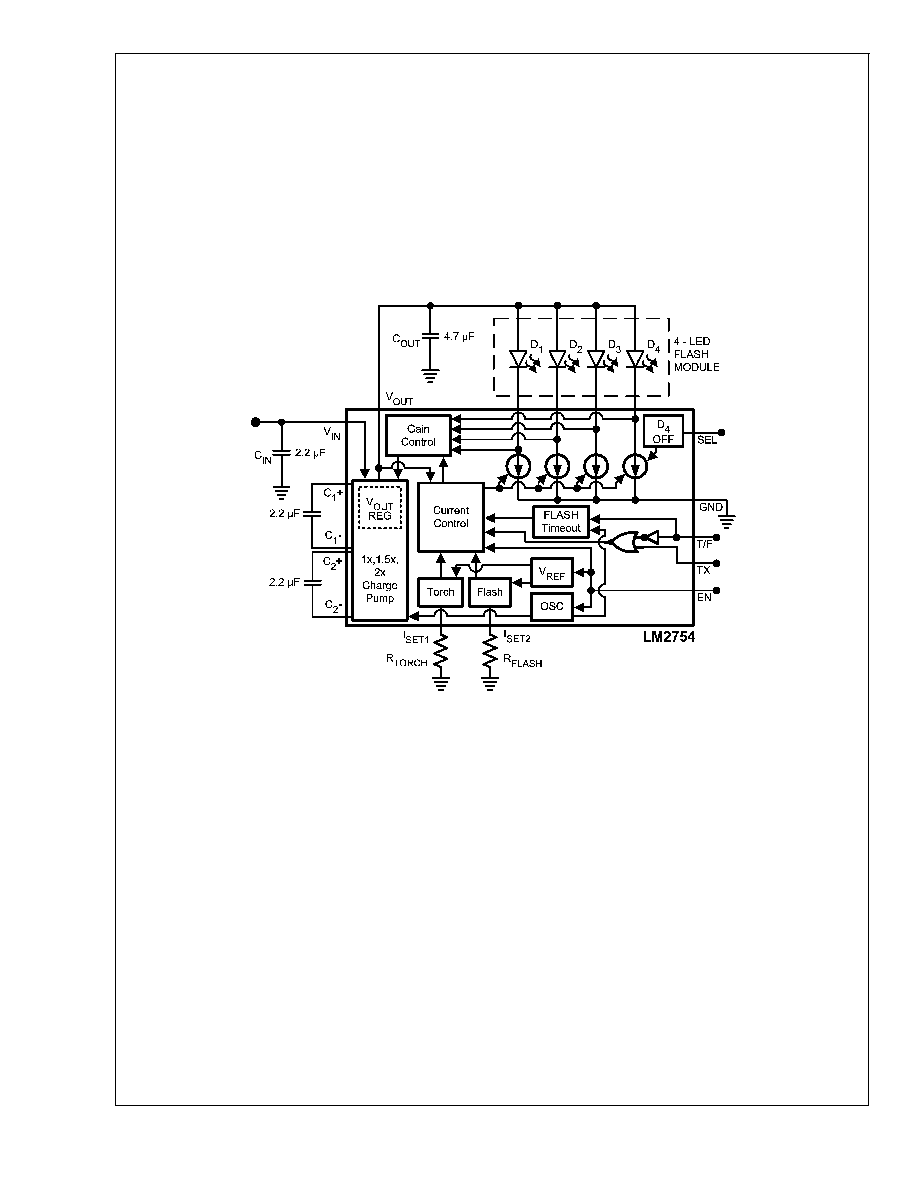
Block Diagram
20202803
LM2754
www.national.com
4
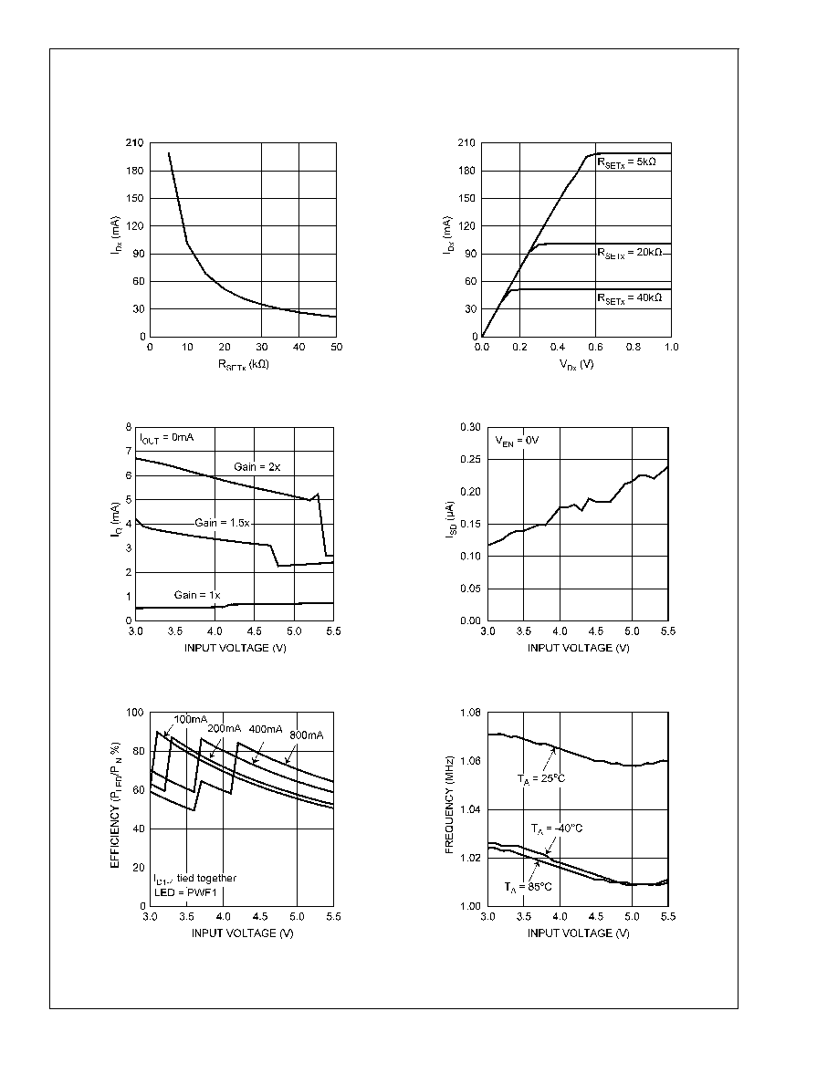
Typical Performance Characteristics
Unless otherwise specified: T
A
= 25°C, V
Dx
= 1V, V
(IN, INSW)
=
3.6V, V
EN
= V
IN
, V
T/F
= V
TX
= V
SEL
= 0V, C
IN
= C
1
= C
2
= 2.2µF, C
OUT
= 4.7µF. Capacitors are low-ESR multi-layer ceramic
capacitors (MLCC's).
Dx Current vs. R
SET
Dx Current vs. Headroom Voltage
20202804
20202805
Quiescent Current vs. Input Voltage
Shutdown Current vs. Input Voltage
20202806
20202807
Efficiency vs. Input Voltage
Oscillator Frequency vs. Input Voltage
20202808
20202809
LM2754
www.national.com
5
Document Outline