LM2787
Low Noise Regulated Switched Capacitor Voltage
Inverter in micro SMD
General Description
The LM2787 CMOS Negative Regulated Switched Capacitor
Voltage Inverter delivers a very low noise adjustable output
for an input voltage in the range of +2.7V to +5.5V. Four low
cost capacitors are used in this circuit to provide up to 10mA
of output current. The regulated output for the LM2787 is
adjustable between -1.5V and -5.2V. The LM2787 operates
at 260 kHz (typical) switching frequency to reduce output
resistance and voltage ripple. With an operating current of
only 400 µA (charge pump power efficiency greater than
90% with most loads) and 0.05 µA typical shutdown current,
the LM2787 provides ideal performance for cellular phone
power amplifier bias and other low current, low noise nega-
tive voltage needs. The device comes in small 8-Bump micro
SMD and thin micro SMD packages.
Features
n
Inverts and regulates the input supply voltage
n
Small 8-Bump micro SMD and thin micro SMD
packages
n
91% typical charge pump power efficiency at 10mA
n
Low output ripple
n
Shutdown lowers Quiescent current to 0.05 µA (typical)
Applications
n
Wireless Communication Systems
n
Cellular Phone Power Amplifier Biasing
n
Interface Power Supplies
n
Handheld Instrumentation
n
Laptop Computers and PDA's
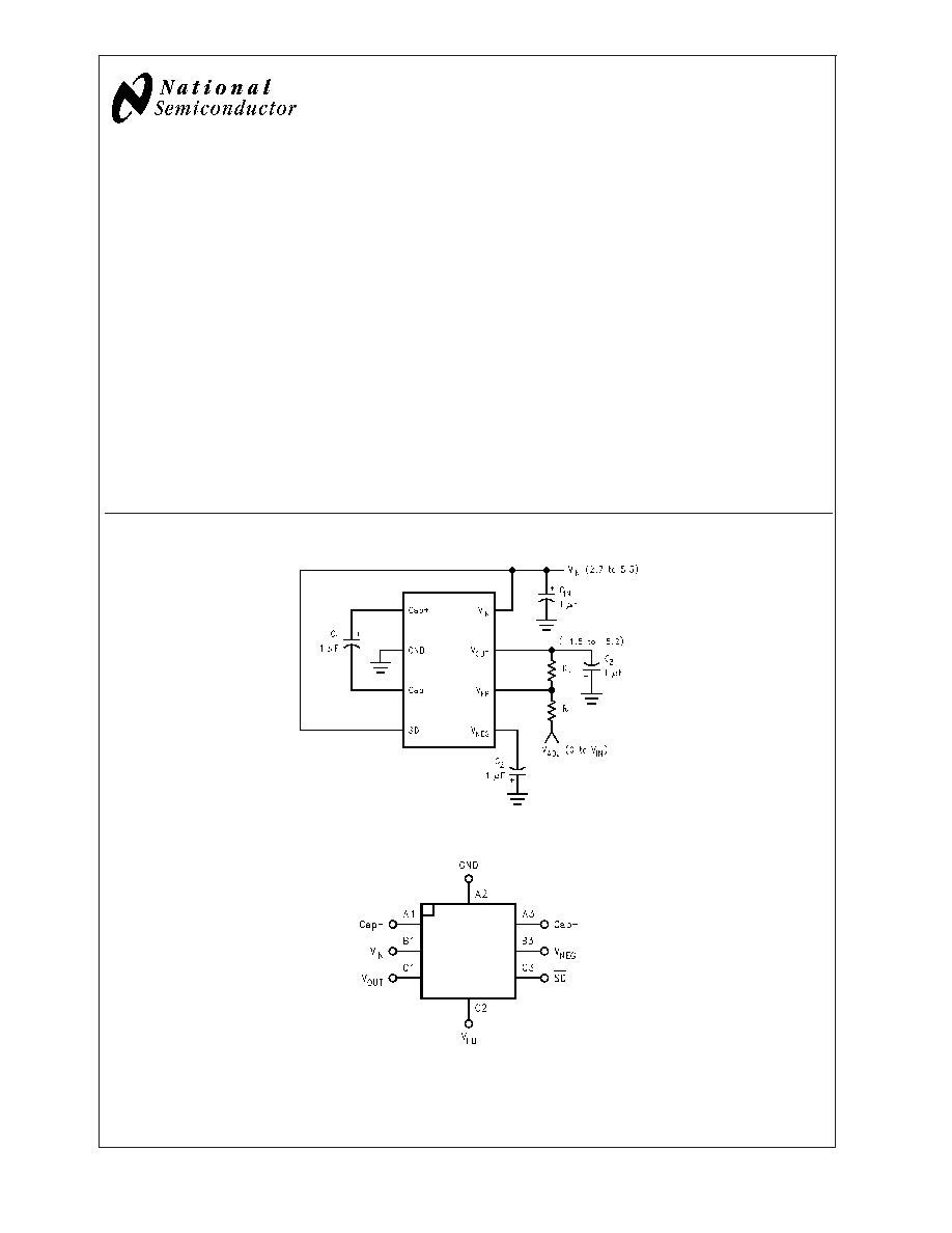
Typical Application Circuit and Connection Diagram
10131325
8-Bump micro SMD (Top View)
10131302
April 2003
LM2787
Low
Noise
Regulated
Switched
Capacitor
V
oltage
Inverter
in
micro
SMD
© 2003 National Semiconductor Corporation
DS101313
www.national.com
Ordering Information
micro SMD
Device Order Number
Package Number
Package Marking
*
Supplies As
LM2787BP
BPA08CCB
S8
Tape and Reel (250 units/reel)
LM2787BPX
BPA08CCB
S8
Tape and Reel (3000 units/reel)
Thin micro SMD
Device Order Number
Package Number
Package Marking
*
Supplies As
LM2787TP
TPA08CCA
S8
Tape and Reel (250 units/reel)
LM2787TPX
TPA08CCA
S8
Tape and Reel (3000 units/reel)
Note: * The small physical size of the micro SMD package does not allow for
the full part number marking. Devices will be marked with the desig-
nation shown in the column Package Marking.
Pin Descriptions
Pin No.
Name
Function
A1
Cap+
Positive terminal for C
1
.
B1
V
IN
Positive power supply input.
C1
V
OUT
Regulated negative output voltage.
C2
V
FB
Feedback input. Connect V
FB
to an external resistor divider between V
OUT
and a positive
adjust voltage V
ADJ
(0
V
ADJ
V
IN
). DO NOT leave unconnected.
C3
SD
Active low, logic-level shutdown input.
B3
V
NEG
Negative unregulated output voltage.
A3
Cap-
Negative terminal for C
1
.
A2
GND
Ground.
LM2787
www.national.com
2
Absolute Maximum Ratings
(Note 1)
If Military/Aerospace specified devices are required,
please contact the National Semiconductor Sales Office/
Distributors for availability and specifications.
Supply Voltage (V
IN
to GND or GND
to OUT)
+ 5.8V
SD
(GND - 0.3V) to
(V
IN
+ 0.3V)
V
NEG
and V
OUT
Continuous Output
Current
10mA
V
OUT
Short-Circuit Duration to GND
(Note 2)
1 sec.
Continuous Power Dissipation (T
A
=
25∞C) (Note 3)
600mW
T
JMAX
(Note 3)
150∞C
JA
(Note 3)
220∞C/W
Operating Input Voltage Range
2.7V to 5.5V
Operating Output Current Range
0mA to 10mA
Operating Ambient
-40∞C to 85∞C
Temp. Range
Operating Junction Temp. Range
-40∞C to 110∞C
Storage Temperature
-65∞C to 150∞C
Lead Temp. (Soldering, 10 sec.)
300∞C
ESD Rating (Note 4)
2kV
Electrical Characteristics
Limits with standard typeface apply for T
J
= 25∞C, and limits in boldface type apply over the full temperature range. Unless
otherwise specified V
IN
= 3.6V, C
1
= C
2
= C
3
= 1µF.
Symbol
Parameter
Conditions
Min
Typ
Max
Units
I
Q
Supply Current
Open Circuit, No Load
400
950
µA
I
SD
Shutdown Supply Current
0.05
1
µA
F
SW
Switching Frequency
(Note 5)
V
IN
= 3.6V
140
260
450
kHz
POWER
Power Efficiency at V
NEG
I
L
= 3.6mA
I
L
= 10mA
94
91
%
T
START
Start Up time
120
600
µs
R
NEG
Output Resistance to V
NEG
(Note 6)
30
V
R
Output Voltage Ripple
(Note 7)
I
L
=2.5mA, V
OUT
= -2.7V
I
L
= 10mA, V
OUT
= -3.8V
1
mV
V
FB
Feedback Pin Reference
Voltage
I
L
= 2.5mA (Note 8)
-1.25
-1.20
-1.15
V
V
OUT
Adjustable Output Voltage
5.5V
V
IN
2.7V, 2.5mA I
L
5.5V
V
IN
3.0V, 10mA I
L
0mA
- (V
IN
-0.3V)
- (V
IN
-1.2V)
V
Load Regulation
0 to 10mA, V
OUT
= - 2.4V
5
mV/mA
Line Regulation
5.5V
V
IN
2.7V, I
L
= 2.5mA
1
mV/V
V
IH
Shutdown Pin Input Voltage
High
5.5V
V
IN
2.7V
2.4
V
V
IL
Shutdown Pin Input Voltage
Low
5.5V
V
IN
2.7V
0.8
V
Note 1: Absolute Maximum Ratings indicate limits beyond which damage to the device may occur. Electrical specifications do not apply when operating the device
beyond its rated operating conditions.
Note 2: OUT may be shorted to GND for one second without damage. However, shorting OUT to V
IN
may damage the device and must be avoided. Also, for
temperatures above T
A
= 85∞C, OUT must not be shorted to GND or V
IN
or device may be damaged.
Note 3: The maximum power dissipation must be de-rated at elevated temperatures and is limited by T
JMAX
(maximum junction temperature), T
A
(ambient
temperature) and
JA
(junction-to-ambient thermal resistance). The maximum power dissipation at any temperature is:
PDiss
MAX
= (T
JMAX
-- T
A
)/
JA
up to the value listed in the Absolute Maximum Ratings.
Note 4: Rating is for the human body model, a 100pF capacitor discharged through a 1.5 k
resistor into each pin.
Note 5: The output switches operate at one half the oscillator frequency, f
OSC
= 2f
SW
.
Note 6: Current drawn from V
NEG
pin decreases power efficiency and will increase output voltage ripple.
Note 7: In the test circuit, capacitors C
1
, C
2
, and C
3
are 1µF, 0.30
maximum ESR capacitors. Capacitors with higher ESR will increase output resistance, increase
output voltage ripple, and reduce efficiency.
Note 8: The feedback resistors R1 and R2 are 200k
resistors.
LM2787
www.national.com
3
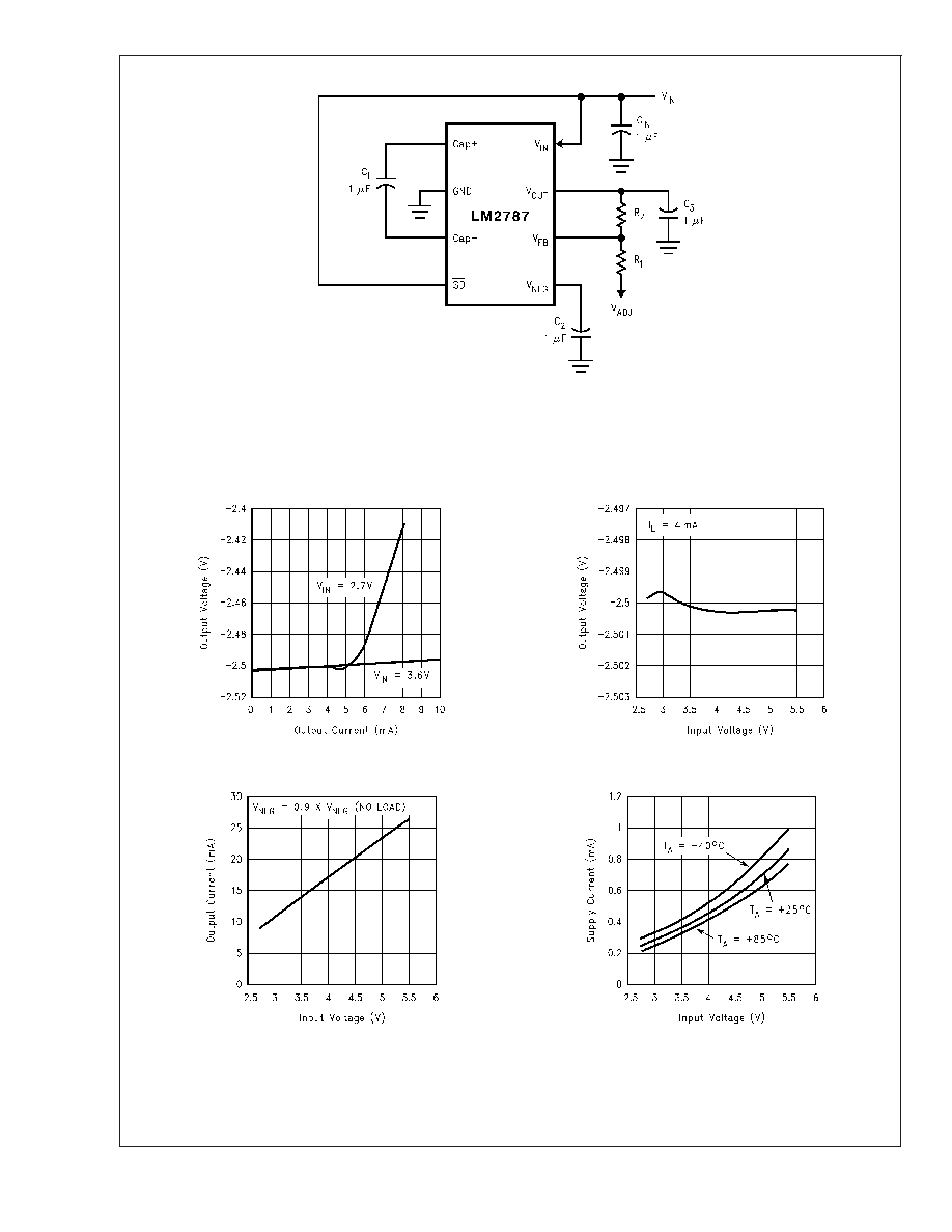
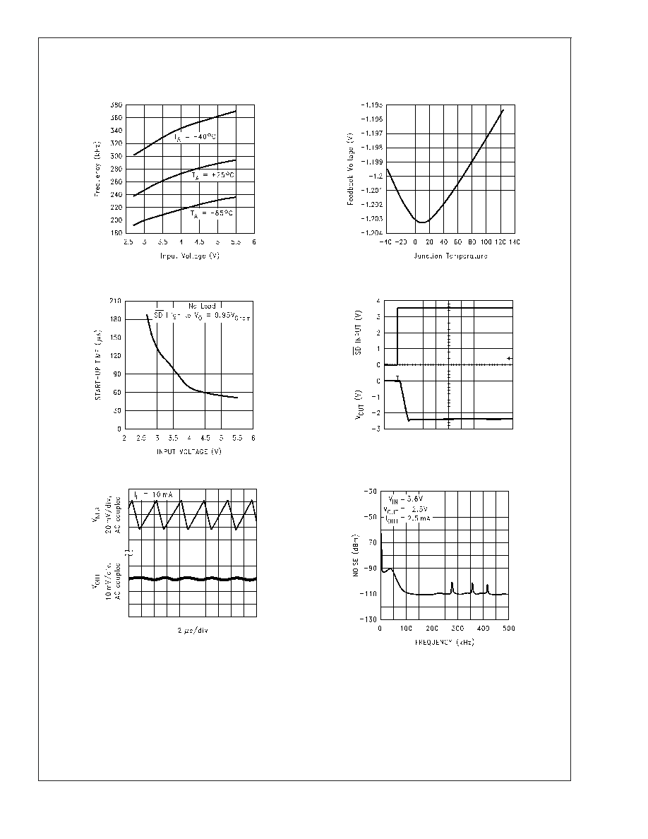
Typical Performance Characteristics
Unless otherwise specified, T
A
= 25∞C, V
OUT
= -2.5V.
Output Voltage vs. Output Current
Output Voltage vs. Input Voltage
10131305
10131306
Maximum V
NEG
Current vs. Input Voltage
No Load Supply Current vs. Input Voltage
10131308
10131309
10131326
FIGURE 1. Standard Application Circuit
LM2787
www.national.com
4