LM2791
Current Regulated Switched Capacitor LED Driver with
Analog Brightness Control
General Description
The LM2791 is a CMOS charge-pump voltage doubler and
regulator that provides two regulated current sources. The
LM2791 is designed to drive two white (or blue) LEDs with
matched currents (within
±
0.3%) to produce balanced light
sources for display backlights. They accept an input voltage
range from 3V to 5.8V and maintain a constant current
determined by an external set resistor.
The LM2791 delivers up to 36mA of load current to accom-
modate two high forward voltage (typically white) LEDs. The
switching frequency is 450kHz (min.) to keep the conducted
noise spectrum away from sensitive frequencies within por-
table RF devices.
In the LM2791, brightness is controlled by applying a voltage
between GND and 3.0V to the BRGT pin. The LM2791 is
available in active high or low shutdown versions. The shut-
down pin reduces the operating current to 1µA (max.).
The LM2791 is available in a 10 pin leadless leadframe
(LLP) CSP package.
Features
n
Output matching of
±
0.3%
n
Drives up to two LED's
n
3V to 5.8V Input Voltage
n
Up to 36mA output current
n
Soft start limits inrush current
n
Analog brightness control
n
Separate shutdown input
n
Very small solution size - no inductor
n
0.7mA typical operating current
n
1µA (max.) shutdown current
n
450kHz switching frequency (min.)
n
Linear regulation generates predictable noise spectrum
n
LLP-10 package: 3mm X 3mm X 0.8mm
Applications
n
White LED Display Backlights
n
White LED Keypad Backlights
n
1-Cell Li-Ion battery-operated equipment including
PDAs, hand-held PCs, cellular phones
n
Flat Panel Dispalys
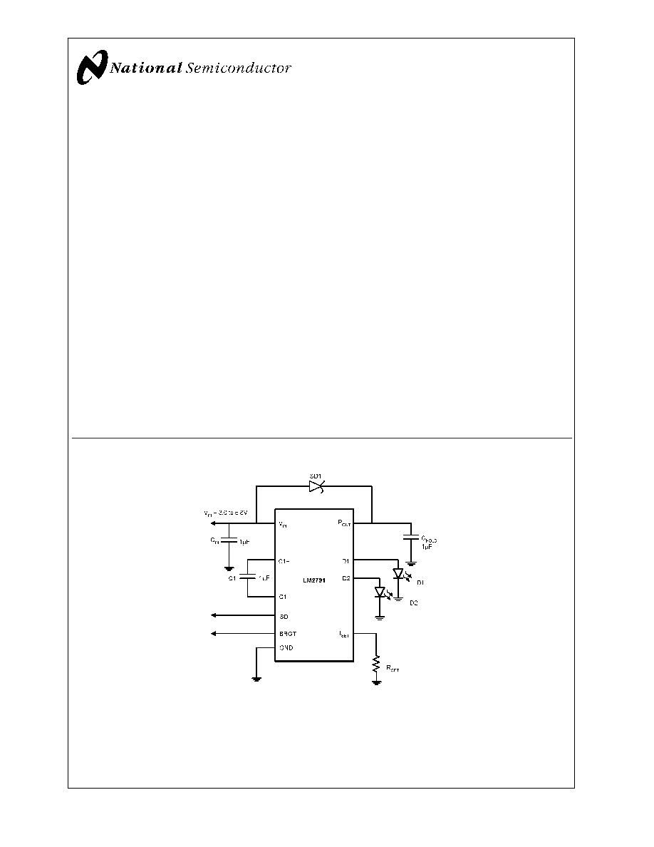
Basic Application Circuit
20018301
July 2002
LM2791
Current
Regulated
Switched
Capacitor
LED
Driver
with
Analog
Brightness
Control
© 2002 National Semiconductor Corporation
DS200183
www.national.com
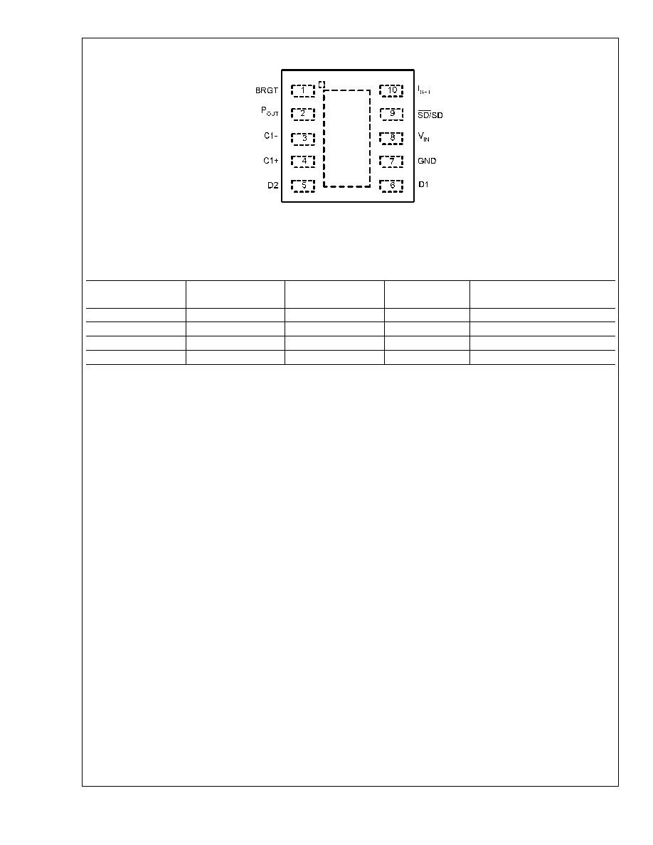
Connection Diagram
20018303
Top View
10-Lead LLP
Ordering Information
Order Number
Shutdown Polarity
NSC Package
Drawing
Package
Marking
Supplied As
LM2791LD-L
Active Low
LLP-10
SNB
1000 Units, Tape and Reel
LM2791LDX-L
Active Low
LLP-10
SNB
4500 Units, Tape and Reel
LM2791LD-H
Active High
LLP-10
SLB
1000 Units, Tape and Reel
LM2791LDX-H
Active High
LLP-10
SLB
4500 Units, Tape and Reel
LM2791
www.national.com
2
Pin Description
Pin
Name
Function
1
BRGT
Variable voltage input controls output current.
2
P
OUT
Charge pump output.
3
C1-
Connect this pin to the negative terminal of C1.
4
C1+
Connect this pin to the positive terminal of C1.
5
D2
Current source outputs. Connect directly to LED.
6
D1
Current source outputs. Connect directly to LED.
7
GND
Power supply ground input.
8
V
IN
Power supply voltage input.
9
SD/SD
Shutdown input. Device operation is inhibited when pin is asserted.
10
I
SET
Current Sense Input. Connect resistor to ground to set constant current through LED.
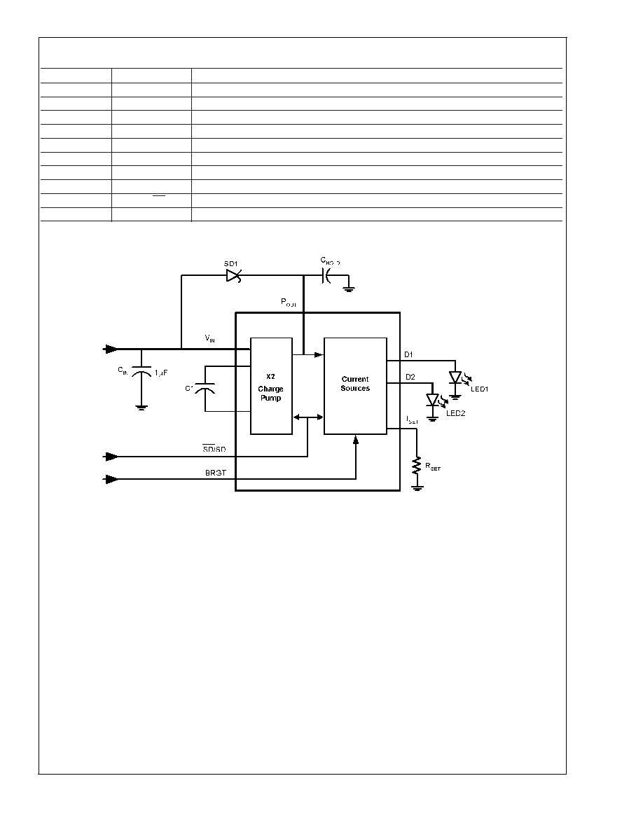
Block Diagram
20018302
LM2791
www.national.com
3
Absolute Maximum Ratings
(Note 1)
If Military/Aerospace specified devices are required,
please contact the National Semiconductor Sales Office/
Distributors for availability and specifications.
V
IN
-0.3 to 6V
BRGT, SD
-0.3 to (V
IN
+0.2V)
Power Dissipation(Note 2)
400 mW
T
JMAX
(Note 2)
150∞C
JA
(Note 7)
55∞C/W
Storge Temperature
-65∞C to +100∞C
Lead Temp. (Soldering, 5 sec.)
260∞C
ESD Rating
Human Body Model
2KV
Machine Model
200V
Operating Conditions
Input Voltage (V
IN
)
3.0V to 5.8V
BRGT
0 to 3.0V
Ambient Temperature (T
A
)
-30∞C to +85∞C
Junction Temperature (T
J
)
-30∞C to +100∞C
Electrical Characteristics
Limits in standard typeface are for T
J
= 25∞C and limits in boldface type apply over the full Operating Temperature Range.
Unless otherwise specified, C
1
= C
IN
= C
HOLD
= 1 µF, V
IN
= 3.6V, V
DIODE
= 3.6V, R
SET
= 332
, BRGT pin = 0V.
Symbol
Parameter
Conditions
Min
Typ
Max
Units
I
DX
Diode Current at ID1,2
V
IN
= 3V, R
SET
= 270
16.5
18
mA
Available Current at Output Dx
V
IN
= 3V
14.5
V
IN
= 3.3V
12.8
15.1
17.7
V
IN
= 3.6V
13.3
15.7
18.4
V
IN
= 4.4V
16.8
I
Dx
Load Regulation at Output Dx
V
IN
=3.6V
V
DX
=3.0V
V
DX
=4.0V
16
15.4
mA
I
DX
Line Regulation of Dx Output
Current
3.3V
V
IN
4.4V
V
DX
= 3.6V
15.7
mA
I
D-MATCH
Current Matching Between Any
Two Outputs
3.0V
V
IN
4.4V
V
D1
, V
D2
= 3.6V
0.3
%
I
Q
Quiescent Supply Current
3.0V
V
IN
4.4V, Active, No
Load Current
0.7
2
mA
I
SD
Shutdown Supply Current
3.0V
V
IN
5.5V, Shutdown at
85∞C
0.1
0.3
1
µA
V
IH
SD Input Logic High
3.0V
V
IN
5.5V, (Note 5)
0.8V
IN
V
V
IL
SD Input Logic Low
3.0V
V
IN
5.5V, (Note 5)
0.2V
IN
V
I
LEAK-SD
SD Input Leakage Current
0V
V
SD
V
IN
0.1
µA
R
BRGT
BRGT Input Resistance
250
k
I
SET
I
SET
Pin Output Current
I
Dx
/25
mA
f
SW
Switching Frequency (Note 4)
3.0V
V
IN
4.4V
450
650
850
kHz
t
START
Startup Time(Note 6)
I
Dx
= 90% steady state
10
µs
Note 1: Absolute maximum ratings indicate limits beyond which damage to the device may occur. Electrical specifications do not apply when operating the device
beyond its rated operating conditions.
Note 2: D1 and D2 may be shorted to GND without damage. P
OUT
may be shorted to GND for 1sec without damage.
Note 3: In the test circuit, all capacitors are 1.0µF, 0.3
maximum ESR capacitors. Capacitors with higher ESR will increase output resistance, reduce output
voltage and efficiency.
Note 4: The output switches operate at one half of the oscillator frequency, f
OSC
= 2f
SW
.
Note 5: The interanl thresholds of the shutdown bar are set at about 40% of V
IN
.
Note 6: This electrical specification is guaranteed by design.
Note 7: For more inforamtion regarding the LLP package, please refer to National Semiconductor Application note AN1187
LM2791
www.national.com
4

Typical Performance Characteristics
Unless otherwise specified, C1 = C
IN
, C
HOLD
= 1uF, V
IN
= 3.6V,
V
DIODE
= 3.6V, BRGT pin =0V, R
SET
= 330
Supply Current at No Load
Supply Current vs Supply Voltage
20018305
20018312
SD-Threshold
I
DIODE
vs V
DIODE
20018308
20018310
Diode Current vs. Temperature
I
DIODE
vs R
Set
20018320
20018311
LM2791
www.national.com
5