LM27951
White LED Adaptive 1.5X/1X Switched Capacitor Current
Driver
General Description
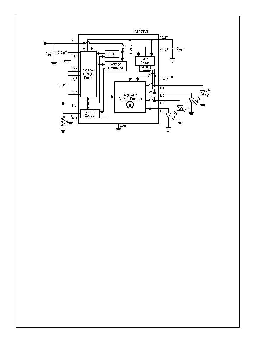
The LM27951 is a switched capacitor white-LED driver ca-
pable of driving up to 4 LEDs with 30mA through each LED.
Its 4 tightly regulated current sources ensure excellent LED
current and brightness matching. LED drive current is pro-
grammed by an external sense resistor. The LM27951 oper-
ates over an input voltage range from 3.0V to 5.5V and
requires only four low-cost ceramic capacitors.
The LM27951 provides excellent efficiency without the use
of an inductor by operating the charge pump in a gain of 3/2,
or in a gain of 1. Maximum efficiency is achieved over the
input voltage range by actively selecting the proper gain
based on the LED forward voltage requirements.
The LM27951 uses constant frequency pre-regulation to
minimize conducted noise on the input. It has a fixed 750kHz
switching frequency optimized for portable applications. The
LM27951 consumes less than 1µA of supply current when
shut down.
The LM27951 is available in a 14-pin No-Pullback Leadless
Leadframe Package: LLP-14.
Features
n
Drives up to 4 LEDs with up to 30mA each
n
Regulated current sources with 0.2%(typ.) matching
n
3/2x, 1x Gain transition based on LED V
F
n
Peak Efficiency Over 85%
n
Input Voltage Range: 3.0V to 5.5V
n
PWM Brightness Control
n
Very Small Solution Size - NO INDUCTOR
n
Fixed 750kHz Switching Frequency
n
<
1µA Shutdown Current
n
14-pin LLP Package: 4.0mm X 3.0mm X 0.8mm
Applications
n
White LED Display Backlights
n
White LED Keypad Backlights
n
General Purpose LED Lighting
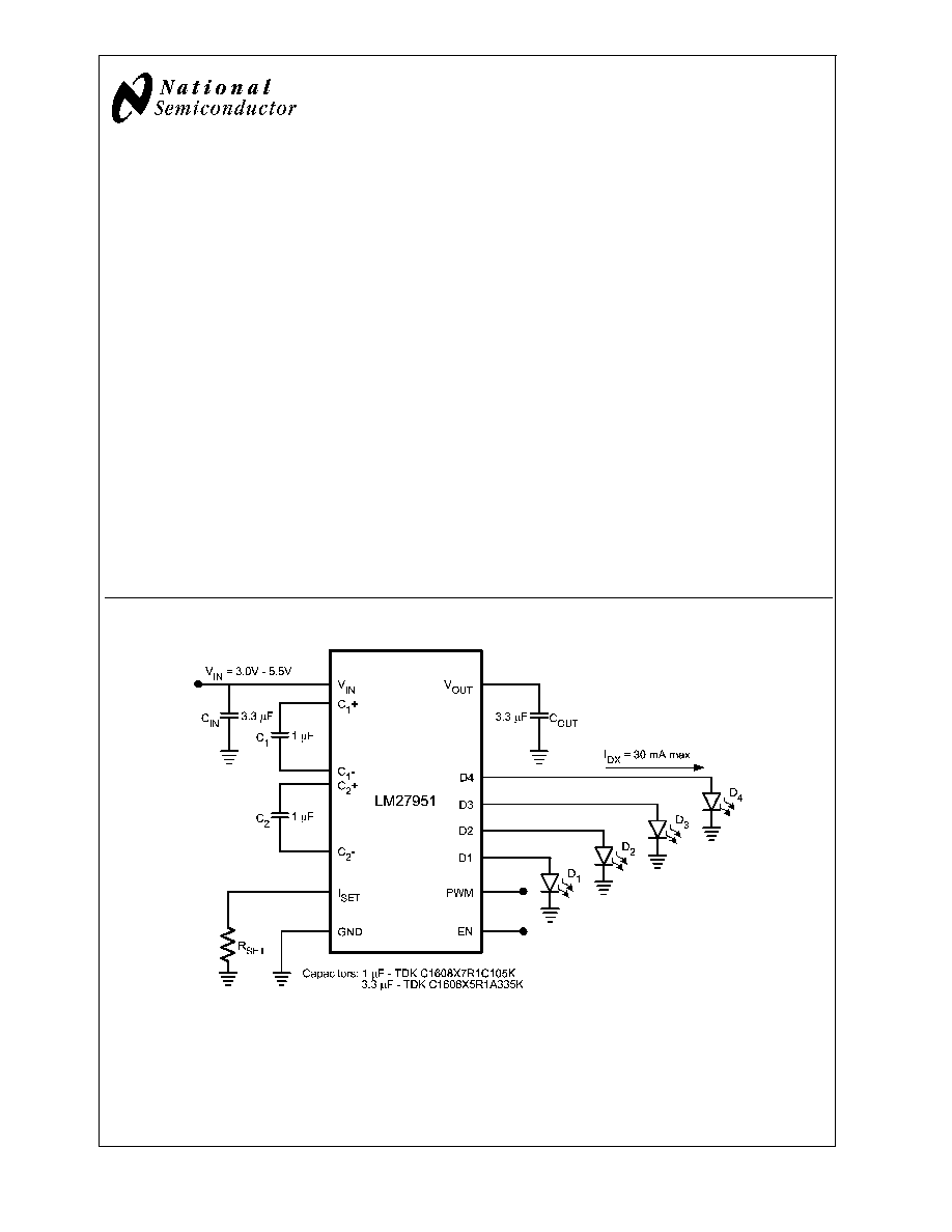
Typical Application Circuit
20171701
November 2005
LM27951
White
LED
Adaptive
1.5X/1X
Switched
Capacitor
Current
Driver
© 2005 National Semiconductor Corporation
DS201717
www.national.com
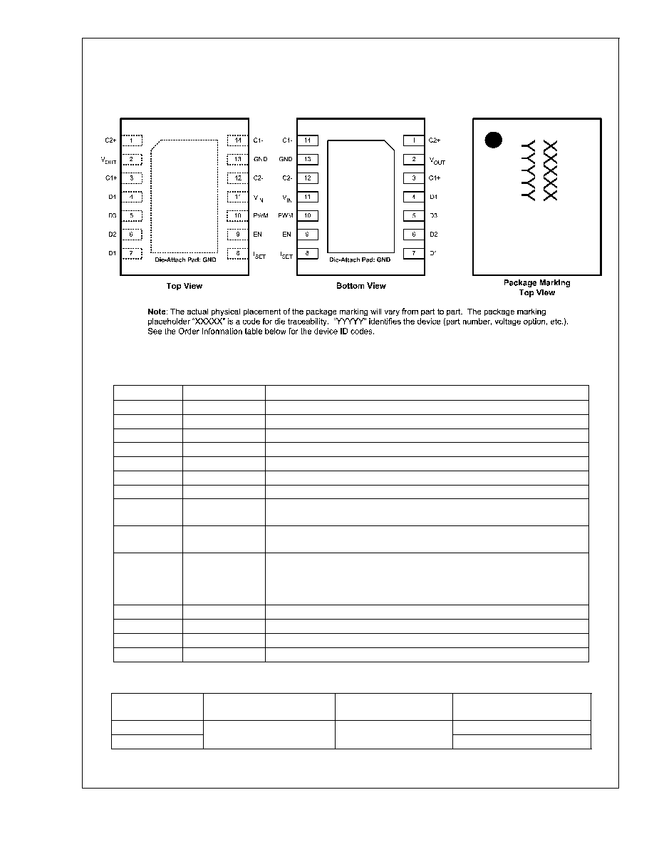
Connection Diagram
LM27951
14-pin No-Pullback Leadless Leadframe Package (LLP-14)
4mm x 3mm x 0.8mm
NS Package Number SDA14A
20171702
Pin Descriptions
Pin
Name
Description
1
C2+
Flying Capacitor C2 Connection
2
V
OUT
Pre-Regulated Charge Pump Output
3
C1+
Flying Capacitor C1 Connection
4
D4
Regulated Current Source Output.
5
D3
Regulated Current Source Output.
6
D2
Regulated Current Source Output.
7
D1
Regulated Current Source Output.
8
I
SET
Current Set Input. Placing a resistor (R
SET
) between this pin and GND sets
the LED current for all the LEDs. LED Current = 200 x (1.25V ÷ R
SET
).
9
EN
Enable Logic Input Pin. Logic Low = Shut Down, Logic High = Enabled. There
is a 150k
(typ.) resistor connected internally between the EN pin and GND.
10
PWM
Current Source Modulation Logic Input Pin. Logic Low = Off, Logic High = On.
Applying a Pulse Width Modulated (PWM) signal to this pin allows the
regulated current sources to be modulated without shutting down the internal
Charge Pump and the V
OUT
node.
11
V
IN
Input Supply Range: 3.0V to 5.5V.
12
C2-
Flying Capacitor C2 Connection.
13
GND
Power Supply Ground Connection.
14
C1-
Flying Capacitor C1 Connection.
Ordering Information
Order Number
Package Description
Package Marking
Supplied as Tape and Reel
(Units)
LM27951SD
No-Pullback
LLP-14
XXXXX = ¢Z¢2¢X
YYYYY = D006B
1000
LM27951SDX
4500
LM27951
www.national.com
2
Absolute Maximum Ratings
(Notes 1, 2)
If Military/Aerospace specified devices are required,
please contact the National Semiconductor Sales Office/
Distributors for availability and specifications.
V
IN
-0.3V to 6.0V
EN, PWM
-0.3V to (V
IN
+ 0.3V)
w/ 6.0V max
Continuous Power Dissipation
(Note 3)
Internally Limited
Junction Temperature
(T
J-MAX-ABS
)
150°C
Storage Temperature Range
-65°C to 150°C
Lead Temp. (Soldering, 5 sec.)
260°C
ESD Rating (Note 4)
Human Body Model
2kV
Operating Ratings
(Notes 2, 7)
Input Voltage V
IN
3.0V to 5.5V
LED Voltage Range
2.5V to 3.9V
Junction Temperature Range (T
J
)
-40°C to +115°C
Ambient Temperature Range (T
A
)
(Note 5)
-40°C to +85 °C
Thermal Information
Junction-to-Ambient Thermal Resistance,
LLP-14 Package (
JA
)
(Note 6)
45°C/W
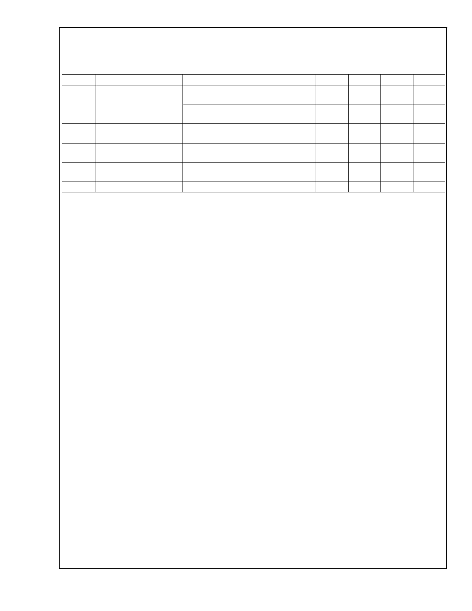
Electrical Characteristics
(Notes 2, 7)
Limits in standard typeface are for T
A
= 25°C, and limits in boldface type apply over the full operating junction temperature
range (-40°C to +85 °C). Unless otherwise noted, specifications apply to the LM27951 Typical Application Circuit (pg.1) with V
IN
= 3.6V, V(EN) = 1.8V, V(PWM) = 1.8V, 4 LEDs, V
DX
= 3.6V, C
IN
= C
OUT
= 3.3µF, C
1
= C
2
= 1µF, R
SET
= 12.5k
(Note 8)
Symbol
Parameter
Conditions
Min
Typ
Max
Units
I
DX
LED Current Regulation
3.0V
V
IN
5.5V
R
SET
= 12.5k
I
VOUT
= 0mA
18.4
(-8%)
20
21.6
(+8%)
mA
3.0V
V
IN
5.5V
R
SET
= 8.32k
I
VOUT
= 0mA
30
3.0V
V
IN
5.5V
R
SET
= 24.9k
I
VOUT
= 0mA
10
I
D-MATCH
LED Current Matching
(Note 9)
R
SET
= 8.32k
0.2
1.5
%
I
Q
Quiescent Supply Current
D
(1-4)
= OPEN
R
SET
= OPEN
1.5
1.9
mA
I
SD
Shutdown Supply Current
3.0V
V
IN
5.5V
V(EN) = 0V
0.1
1
µA
V
SET
I
SET
Pin Voltage
3.0V
V
IN
5.5V
1.25
V
I
DX
/ I
SET
Output Current to Current
Set Ratio
200
V
HR
Current Source Voltage
Headroom Requirement
(Note 10)
I
DX
= 95% I
DX
(nom.)
R
SET
= 8.32k
(I
DX
nom. = 30mA)
360
mV
I
DX
= 95% I
DX
(nom.)
R
SET
= 12.5k
(I
DX
nom. = 20mA)
240
f
SW
Switching Frequency
525
(-30%)
750
975
(+30%)
kHz
V
IH
Logic Input High
Input Pins: EN, PWM
3.0V
V
IN
5.5V
1.0
V
IN
V
V
IL
Logic Input Low
Input Pins: EN, PWM
3.0V
V
IN
5.5V
0
0.4
LM27951
www.national.com
3
Electrical Characteristics
(Notes 2, 7)
(Continued)
Limits in standard typeface are for T
A
= 25°C, and limits in boldface type apply over the full operating junction temperature
range (-40°C to +85 °C). Unless otherwise noted, specifications apply to the LM27951 Typical Application Circuit (pg.1) with V
IN
= 3.6V, V(EN) = 1.8V, V(PWM) = 1.8V, 4 LEDs, V
DX
= 3.6V, C
IN
= C
OUT
= 3.3µF, C
1
= C
2
= 1µF, R
SET
= 12.5k
(Note 8)
Symbol
Parameter
Conditions
Min
Typ
Max
Units
I
IH
Logic Input High Current
Input Pin: PWM
V(PWM) = 1.8V
10
nA
Input Pin: EN
V(EN) = 1.8V (Note 11)
12
µA
I
IL
Logic Input Low Current
Input Pins: EN, PWM
V(EN, PWM) = 0V
10
nA
R
OUT
Charge Pump Output
Resistance (Note 12)
3.3
V
GDX
1x to 3/2x Gain Transition
Voltage Threshold on V
DX
V
DX
Falling
500
mV
t
ON
Startup Time
I
DX
= 90% steady state
330
µs
Note 1: Absolute Maximum Ratings indicate limits beyond which damage to the component may occur. Operating Ratings are conditions under which operation of
the device is guaranteed. Operating Ratings do not imply guaranteed performance limits. For guaranteed performance limits and associated test conditions, see the
Electrical Characteristics tables.
Note 2: All voltages are with respect to the potential at the GND pin.
Note 3: Internal thermal shutdown circuitry protects the device from permanent damage. Thermal shutdown engages at T
J
=150°C (typ.) and disengages at T
J
=
140°C (typ.).
Note 4: The Human-body model is a 100 pF capacitor discharged through a 1.5k
resistor into each pin.
Note 5: In applications where high power dissipation and/or poor package thermal resistance is present, the maximum ambient temperature may have to be
derated. Maximum ambient temperature (T
A-MAX
) is dependent on the maximum operation junction temperature (T
J-MAX-OP
= 115
o
C), the maximum power
dissipation of the device in the application (P
D-MAX
), and the junction-to ambient thermal resistance of the part/package in the application (
JA
), as given by the
following equation: T
A-MAX
= T
J-MAX-OP
- (
JA
x P
D-MAX
).
Note 6: Junction-to-ambient thermal resistance (
JA
) is taken from a thermal modeling result, performed under the conditions and guidelines set forth in the JEDEC
standard JESD51-7. The test board is a 4 layer FR-4 board measuring 102mm x 76mm x 1.6mm with a 2 x 1 array of thermal vias. The ground plane on the board
is 50mm x 50mm. Thickness of copper layers are 36µm/18µm /18µm/36µm (1.5oz/1oz/1oz/1.5oz). Ambient temperature in simulation is 22°C, still air. Power
dissipation is 1W.
The value of
JA
of the LM27951 in LLP-14 could fall in a range as wide as 45
o
C/W to 150
o
C/W (if not wider), depending on PWB material, layout, and environmental
conditions. In applications where high maximum power dissipation exists (high V
IN
, high I
OUT
), special care must be paid to thermal dissipation issues. For more
information on these topics, please refer to Application Note 1187: Leadless Leadframe Package (LLP) and the Power Efficiency and Power Dissipation
section of this datasheet..
Note 7: Min and Max limits are guaranteed by design, test, or statistical analysis. Typical numbers are not guaranteed, but do represent the most likely norm.
Note 8: C
IN
, C
OUT
, C
1
, C
2
: Low-ESR Surface-Mount Ceramic Capacitors (MLCCs) used in setting electrical characteristics
Note 9: LED Current Matching is based on two calculations: [(I
MAX
- I
AVG
) ÷ I
AVG
] and [(I
AVG
- I
MIN
) ÷ I
AVG
]. I
MAX
and I
MIN
are the highest and lowest respective
Dx currents, and I
AVG
is the average Dx current of all four current sources. The largest number of the two calculations (worst case) is considered the matching figure
for the part. The typical specification provided is the most likely norm of the matching figure for all parts.
Note 10: Headroom Voltage = V
DX
to GND. If headroom voltage requirement is not met, LED current regulation will be compromised.
Note 11: EN Logic Input High Current (I
IH
) is due to a 150k
(typ.) pull-down resistor connected internally between the EN and GND pins.
Note 12: The open loop output resistance (R
OUT
) models all voltage losses in the charge pump. R
OUT
can be used to estimate the voltage at the charge pump
output V
OUT
and the maximum current capability of the device under low V
IN
and high I
OUT
conditions, beyond what is specified in the electrical specifications table:
V
OUT
= (G x V
IN
) - (R
OUT
x I
OUT
). In the equation, G is the charge pump gain mode, and I
OUT
is the total output current (sum of all active Dx current sources and
all current drawn from V
OUT
).
Note 13: Turn-on time is measured from when the EN signal is pulled high until the output voltage on V
OUT
crosses 90% of its final value.
LM27951
www.national.com
4