 | –≠–ª–µ–∫—Ç—Ä–æ–Ω–Ω—ã–π –∫–æ–º–ø–æ–Ω–µ–Ω—Ç: LM27952 | –°–∫–∞—á–∞—Ç—å:  PDF PDF  ZIP ZIP |
LM27952
White LED Adaptive 1.5X/1X Switched Capacitor Current
Driver
General Description
The LM27952 is a switched capacitor white-LED driver ca-
pable of driving up to 4 LEDs with 30mA through each LED.
Its 4 tightly regulated current sinks ensure excellent LED
current and brightness matching. LED drive current is pro-
grammed by an external sense resistor. The LM27952 oper-
ates over an input voltage range from 3.0V to 5.5V and
requires only four low-cost ceramic capacitors.
The LM27952 provides excellent efficiency without the use
of an inductor by operating the charge pump in a gain of 3/2,
or in a gain of 1. Maximum efficiency is achieved over the
input voltage range by actively selecting the proper gain
based on the LED forward voltage requirements.
The LM27952 uses constant frequency pre-regulation to
minimize conducted noise on the input. It has a fixed 750kHz
switching frequency optimized for portable applications. The
LM27952 consumes less than 1µA of supply current when
shut down.
The LM27952 is available in a 14-pin No-Pullback Leadless
Leadframe Package: LLP-14.
Features
n
Drives up to 4 LEDs with up to 30mA each
n
Regulated current sources with 0.2%(typ.) matching
n
3/2x, 1x Gain transition based on LED V
F
n
Peak Efficiency Over 85%
n
Input Voltage Range: 3.0V to 5.5V
n
PWM Brightness Control
n
Very Small Solution Size - NO INDUCTOR
n
Fixed 750kHz Switching Frequency
n
<
1µA Shutdown Current
n
14-pin LLP Package: 4.0mm X 3.0mm X 0.8mm
Applications
n
White LED Display Backlights
n
White LED Keypad Backlights
n
General Purpose LED Lighting
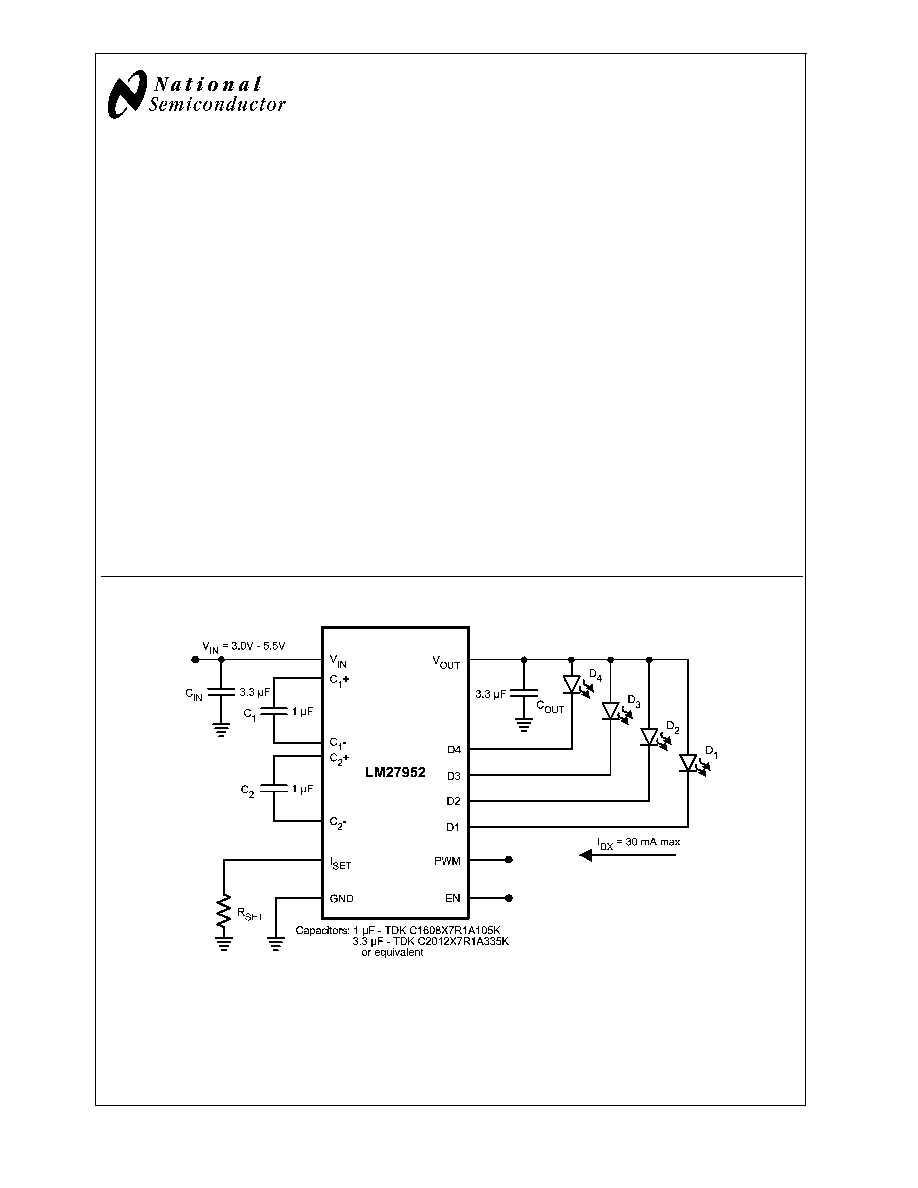
Typical Application Circuit
20148001
May 2005
LM27952
White
LED
Adaptive
1.5X/1X
Switched
Capacitor
Current
Driver
© 2005 National Semiconductor Corporation
DS201480
www.national.com
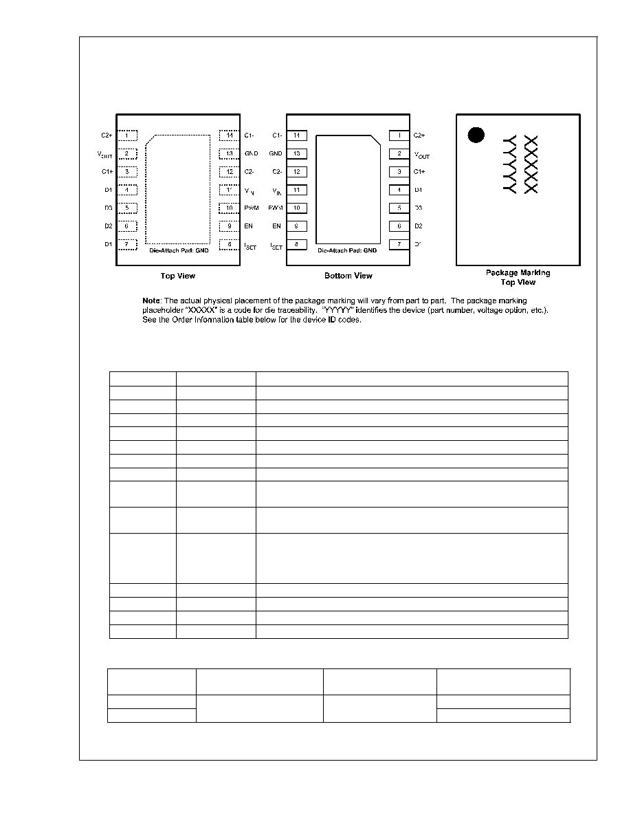
Connection Diagram
LM27952
14-pin No-Pullback Leadless Leadframe Package (LLP-14)
4mm x 3mm x 0.8mm
NS Package Number SDA14A
20148002
Pin Description
Pin
Name
Description
1
C2+
Flying Capacitor C2 Connection
2
V
OUT
Pre-Regulated Charge Pump Output
3
C1+
Flying Capacitor C1 Connection
4
D4
Regulated Current Sink Input.
5
D3
Regulated Current Sink Input.
6
D2
Regulated Current Sink Input.
7
D1
Regulated Current Sink Input.
8
I
SET
Current Set Input. Placing a resistor (R
SET
) between this pin and GND sets
the LED current for all the LEDs. LED Current = 200 x (1.25V ˜ R
SET
).
9
EN
Enable Logic Input Pin. Logic Low = Shut Down, Logic High = Enabled. There
is a 150k
(typ.) resistor connected internally between the EN pin and GND.
10
PWM
Current Sink Modulation Logic Input Pin. Logic Low = Off, Logic High = On.
Applying a Pulse Width Modulated (PWM) signal to this pin allows the
regulated current sinks to be modulated without shutting down the internal
Charge Pump and the V
OUT
node.
11
V
IN
Input Supply Range: 3.0V to 5.5V.
12
C2-
Flying Capacitor C2 Connection.
13
GND
Power Supply Ground Connection.
14
C1-
Flying Capacitor C1 Connection.
Ordering Information
Order Number
Package Description
Package Marking
Supplied as Tape and Reel
(Units)
LM27952SD
No-Pullback
LLP-14
XXXXX
YYYYY = D005B
1000
LM27952SDX
4500
LM27952
www.national.com
2

Absolute Maximum Ratings
(Notes 1, 2)
If Military/Aerospace specified devices are required,
please contact the National Semiconductor Sales Office/
Distributors for availability and specifications.
V
IN
-0.3V to 6.0V
EN, PWM
-0.3V to (V
IN
+ 0.3V)
w/ 6.0V max
Continuous Power Dissipation
(Note 3)
Internally Limited
Junction Temperature
(T
J-MAX-ABS
)
150∞C
Storage Temperature Range
-65∞C to 150∞C
Lead Temp. (Soldering, 5 sec.)
260∞C
ESD Rating (Note 4)
Human Body Model
2kV
Operating Ratings
(Notes 2, 7)
Input Voltage V
IN
3.0V to 5.5V
LED Voltage Range
2.5V to 3.9V
Junction Temperature Range (T
J
)
-40∞C to +115∞C
Ambient Temperature Range (T
A
)
(Note 5)
-40∞C to +85 ∞C
Thermal Information
Junction-to-Ambient Thermal Resistance,
LLP-14 Package (
JA
)
(Note 6)
45∞C/W
Electrical Characteristics
(Notes 2, 7)
Limits in standard typeface are for T
A
= 25∞C, and limits in boldface type apply over the full operating junction temperature
range (-40∞C to +85 ∞C). Unless otherwise noted, specifications apply to the LM27952 Typical Application Circuit (pg.1) with V
IN
= 3.6V, V(EN) = 1.8V, V(PWM) = 1.8V, 4 LEDs, V
DX
= 0.45V, C
IN
= C
OUT
= 3.3µF, C
1
= C
2
= 1µF, R
SET
= 12.5k
(Note 8)
Symbol
Parameter
Conditions
Min
Typ
Max
Units
I
DX
LED Current Regulation
3.0V
V
IN
5.5V
R
SET
= 12.5k
I
VOUT
= 0mA
19.32
(-8%)
21
22.68
(+8%)
mA
3.0V
V
IN
5.5V
R
SET
= 8.32k
I
VOUT
= 0mA
31
3.0V
V
IN
5.5V
R
SET
= 24.9k
I
VOUT
= 0mA
11
I
D-MATCH
LED Current Matching
(Note 9)
R
SET
= 8.32k
0.2
1
%
I
Q
Quiescent Supply Current
D
(1-4)
= OPEN
R
SET
= OPEN
1.3
1.7
mA
I
SD
Shutdown Supply Current
3.0V
V
IN
5.5V
V(EN) = 0V
0.1
1
µA
V
SET
I
SET
Pin Voltage
3.0V
V
IN
5.5V
1.25
V
I
DX
/ I
SET
Output Current to Current
Set Ratio
200
V
HR
Current Sink Voltage
Headroom Requirement
(Note 10)
I
DX
= 95% I
DX
(nom.)
R
SET
= 8.32k
(I
DX
nom. = 31mA)
360
mV
I
DX
= 95% I
DX
(nom.)
R
SET
= 12.5k
(I
DX
nom. = 21mA)
240
f
SW
Switching Frequency
525
(-30%)
750
975
(+30%)
kHz
V
IH
Logic Input High
Input Pins: EN, PWM
3.0V
V
IN
5.5V
1.0
V
IN
V
V
IL
Logic Input Low
Input Pins: EN, PWM
3.0V
V
IN
5.5V
0
0.4
LM27952
www.national.com
3

Electrical Characteristics
(Notes 2, 7)
(Continued)
Limits in standard typeface are for T
A
= 25∞C, and limits in boldface type apply over the full operating junction temperature
range (-40∞C to +85 ∞C). Unless otherwise noted, specifications apply to the LM27952 Typical Application Circuit (pg.1) with V
IN
= 3.6V, V(EN) = 1.8V, V(PWM) = 1.8V, 4 LEDs, V
DX
= 0.45V, C
IN
= C
OUT
= 3.3µF, C
1
= C
2
= 1µF, R
SET
= 12.5k
(Note 8)
Symbol
Parameter
Conditions
Min
Typ
Max
Units
I
IH
Logic Input High Current
Input Pin: PWM
V(PWM) = 1.8V
10
nA
Input Pin: EN
V(EN) = 1.8V (Note 11)
12
µA
I
IL
Logic Input Low Current
Input Pins: EN, PWM
V(EN, PWM) = 0V
10
nA
R
OUT
Charge Pump Output
Resistance (Note 12)
3.3
V
GDX
1x to 3/2x Gain Transition
Voltage Threshold on V
DX
V
DX
Falling
450
mV
t
ON
Startup Time
I
DX
= 90% steady state
330
µs
Note 1: Absolute Maximum Ratings indicate limits beyond which damage to the component may occur. Operating Ratings are conditions under which operation of
the device is guaranteed. Operating Ratings do not imply guaranteed performance limits. For guaranteed performance limits and associated test conditions, see the
Electrical Characteristics tables.
Note 2: All voltages are with respect to the potential at the GND pin.
Note 3: Internal thermal shutdown circuitry protects the device from permanent damage. Thermal shutdown engages at T
J
=150∞C (typ.) and disengages at T
J
=
140∞C (typ.).
Note 4: The Human-body model is a 100 pF capacitor discharged through a 1.5k
resistor into each pin.
Note 5: In applications where high power dissipation and/or poor package thermal resistance is present, the maximum ambient temperature may have to be
derated. Maximum ambient temperature (T
A-MAX
) is dependent on the maximum operation junction temperature (T
J-MAX-OP
= 115
o
C), the maximum power
dissipation of the device in the application (P
D-MAX
), and the junction-to ambient thermal resistance of the part/package in the application (
JA
), as given by the
following equation: T
A-MAX
= T
J-MAX-OP
- (
JA
x P
D-MAX
).
Note 6: Junction-to-ambient thermal resistance (
JA
) is taken from a thermal modeling result, performed under the conditions and guidelines set forth in the JEDEC
standard JESD51-7. The test board is a 4 layer FR-4 board measuring 102mm x 76mm x 1.6mm with a 2 x 1 array of thermal vias. The ground plane on the board
is 50mm x 50mm. Thickness of copper layers are 36µm/18µm /18µm/36µm (1.5oz/1oz/1oz/1.5oz). Ambient temperature in simulation is 22∞C, still air. Power
dissipation is 1W.
The value of
JA
of the LM27952 in LLP-14 could fall in a range as wide as 45
o
C/W to 150
o
C/W (if not wider), depending on PWB material, layout, and environmental
conditions. In applications where high maximum power dissipation exists (high V
IN
, high I
OUT
), special care must be paid to thermal dissipation issues. For more
information on these topics, please refer to Application Note 1187: Leadless Leadframe Package (LLP) and the Power Efficiency and Power Dissipation
section of this datasheet..
Note 7: Min and Max limits are guaranteed by design, test, or statistical analysis. Typical numbers are not guaranteed, but do represent the most likely norm.
Note 8: C
IN
, C
OUT
, C
1
, C
2
: Low-ESR Surface-Mount Ceramic Capacitors (MLCCs) used in setting electrical characteristics
Note 9: LED Current Matching is based on two calculations: [(I
MAX
- I
AVG
) ˜ I
AVG
] and [(I
AVG
- I
MIN
) ˜ I
AVG
]. I
MAX
and I
MIN
are the highest and lowest respective
Dx currents, and I
AVG
is the average Dx current of all four current sinks. The largest number of the two calculations (worst case) is considered the matching figure
for the part. The typical specification provided is the most likely norm of the matching figure for all parts.
Note 10: Headroom Voltage = V
DX
to GND. If headroom voltage requirement is not met, LED current regulation will be compromised.
Note 11: EN Logic Input High Current (I
IH
) is due to a 150k
(typ.) pull-down resistor connected internally between the EN and GND pins.
Note 12: The open loop output resistance (R
OUT
) models all voltage losses in the charge pump. R
OUT
can be used to estimate the voltage at the charge pump
output V
OUT
and the maximum current capability of the device under low V
IN
and high I
OUT
conditions, beyond what is specified in the electrical specifications table:
V
OUT
= (G x V
IN
) - (R
OUT
x I
OUT
). In the equation, G is the charge pump gain mode, and I
OUT
is the total output current (sum of all active Dx current sinks and all
current drawn from V
OUT
).
Note 13: Turn-on time is measured from when the EN signal is pulled high until the output voltage on V
OUT
crosses 90% of its final value.
LM27952
www.national.com
4

Application Information
CIRCUIT DESCRIPTION
The LM27952 is an adaptive 1.5x/1x CMOS charge pump,
optimized for driving white LEDs used in backlighting small-
format displays. It provides four constant current inputs ca-
pable of sinking up to 30mA through each LED. The well-
matched current sinks ensure the current through all the
LEDs are virtually identical, providing a uniform brightness
across the entire display.
Each LED is driven from V
OUT
and connected to one of the
four current sinks. LED drive current is programmed by
connecting a resistor, R
SET
, to the current set pin, I
SET
. LED
brightness is adjusted by applying a Pulse Width Modulated
(PWM) signal to the dedicated PWM input pin.
CHARGE PUMP
The input to the 1.5x/1x charge pump is connected to the V
IN
pin, and the loosely regulated output of the charge pump is
connected to the V
OUT
pin. The recommended input voltage
range of the LM27952 is 3.0V to 5.5V. The device's loosely-
regulated charge pump has both open loop and closed loop
modes of operation. When the device is in open loop, the
voltage at V
OUT
is equal to the gain times the voltage at the
input. When the device is in closed loop, the voltage at V
OUT
is loosely regulated to 4.5V (typ.). The charge pump gain
transitions are actively selected to maintain regulation based
on LED forward voltage and load requirements. This allows
the charge pump to stay in the most efficient gain (1x) over
as much of the input voltage range as possible, reducing the
power consumed from the battery.
SOFT START
The LM27952 contains internal soft-start circuitry to limit
input inrush currents when the part is enabled. Soft start is
implemented internally with a controlled turn-on of the inter-
nal voltage reference. Due to the soft-start circuitry, startup
time of the LM27952 is approximately 330µs (typ.).
ENABLE AND PWM PINS
The LM27952 has 2 logic control pins. Both pins are active-
high logic (HIGH = ON). There is an internal pull-down
resistor (150k
typ.) connected between the enable pin (EN)
and GND. There is no pull-up or pull-down connected to the
Pulse Width Modulated (PWM) pin.
The EN pin is the master enable pin for the part. When the
voltage on this pin is low (
<
0.4V), the part is in shutdown
mode. In this mode, all internal circuitry is OFF and the part
consumes very little supply current (
<
1µA typ.). When the
voltage on the EN pin is high (
>
1.0V), the part will activate
the charge pump and regulate the output voltage to its
nominal value.
The PWM pin serves as a dedicated logic input for LED
brightness control. When the voltage on this pin is low
(
<
0.4V), the current sinks will be turned off and no current
will flow through the LEDs. When the voltage on this pin is
high (
>
1.0V), the currents sinks will turn on and regulate to
the current level set by the resistor connected to the I
SET
pin.
SETTING LED CURRENTS
The current through the four LEDs connected to D
1-4
can be
set to a desired level simply by connecting an appropriately
sized resistor (R
SET
) between the I
SET
pin of the LM27952
and GND. The LED currents are proportional to the current
that flows out of the I
SET
pin and are a factor of 200 times
greater than the I
SET
current. The feedback loop of an inter-
nal amplifier sets the voltage of the I
SET
pin to 1.25V (typ.).
The statements above are simplified in the equations below:
I
Dx
= 200 x(V
SET
/ R
SET
)
R
SET
= 200 x (1.25V / I
Dx
)
ADJUSTING LED BRIGHTNESS (PWM control)
Perceived LED brightness can be adjusted using a PWM
control signal on the LM27952 PWM logic input pin, turning
the current sources ON and OFF at a rate faster than per-
ceptible by the eye. When this is done, the total brightness
perceived is proportional to the duty cycle (D) of the PWM
signal (D = the percentage of time that the LED is on in every
PWM cycle). A simple example: if the LEDs are driven at
15mA each with a PWM signal that has a 50% duty cycle,
perceived LED brightness will be about half as bright as
compared to when the LEDs are driven continuously with
15mA.
The minimum recommended PWM frequency is 100Hz. Fre-
quencies below this may be visibly noticeable as flicker or
blinking. The maximum recommended PWM frequency is
1kHz. Frequencies above this may cause interference with
internal current driver circuitry and/or noise in the audible
range. Due to the regulation control loop, the maximum
frequency and minimum duty cycle applied to the PWM pin
should be chosen such that the minimum ON time is no less
than 30µs in duration. If a PWM signal is applied to the EN
pin instead, the maximum frequency and minimum duty
cycle should be chosen to accommodate both the LM27952
startup time (330µs typ.) and the 30µs control loop delay.
The preferred method to adjust brightness is to keep the
master EN voltage ON continuously and apply a PWM signal
to the dedicated PWM input pin. The benefit of this type of
connection can be best understood with a contrary example.
When a PWM signal is connected to the master enable (EN)
pin, the charge pump repeatedly turns on and off. Every time
the charge pump turns on, there is an inrush of current as the
capacitances, both internal and external, are recharged. This
inrush current results in a current spike and a voltage dip at
the input of the part. By only applying the PWM signal to
PWM logic input pin, the charge pump continuously stays
on, resulting in much lower input noise.
In cases where a PWM signal must be connected to the EN
pin, measures can be taken to reduce the magnitude of the
charge-pump turn-on transient response. More input capaci-
tance, series resistors and/or ferrite beads may provide ben-
efits. If the current spikes and voltage dips can be tolerated,
connecting the PWM signal to the EN pin does provide a
benefit of lower supply current consumption. When the PWM
signal to the EN pin is low, the LM27952 will be shutdown
and input current will only be a few micro-amps. This results
in a lower time-averaged input current than the prior sugges-
tion, where EN is kept on continuously.
MAXIMUM OUTPUT CURRENT, MAXIMUM LED
VOLTAGE, MINIMUM INPUT VOLTAGE
The LM27952 can drive 4 LEDs at 30mA each from an input
voltage as low as 3.0V, so long as the LEDs have a forward
voltage of 3.5V or less (room temperature).
The statement above is a simple example of the LED drive
capabilities of the LM27952. The statement contains key
application parameters required to validate an LED-drive
design using the LM27952: LED current (I
LED
), number of
active LEDs (N), LED forward voltage (V
LED
), and minimum
input voltage (V
IN-MIN
).
LM27952
www.national.com
5