LM27961
Dual-Display White LED Driver with 3/2x Switched
Capacitor Boost
General Description
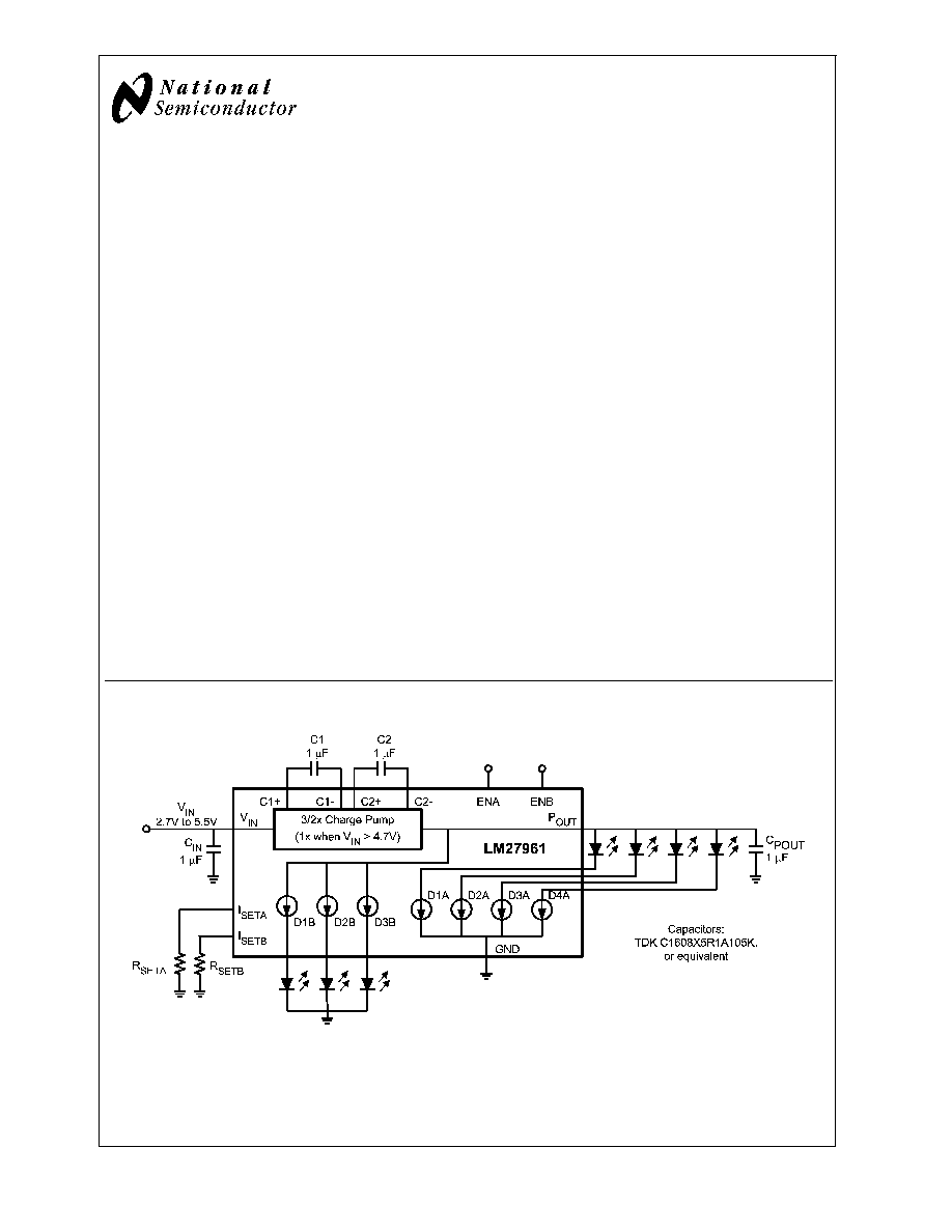
The LM27961 is a charge-pump-based white-LED driver that
is ideal for mobile phone display backlighting. It is intended
to drive 4 LEDs for a main phone display backlight and 3
LEDs for a sub-display backlight. Regulated internal current
sources deliver excellent current and brightness matching in
all LEDs.
The LED driver current sources are split into two indepen-
dently controlled groups. The primary group (Group A) can
be used to backlight a main phone display with up to 4 LEDs.
The low-side current drivers of Group A accommodate
common-anode-type LEDs. The second group (Group B)
can backlight a secondary display with up to 3 LEDs. The
high-side current drivers of Group B accommodate common-
cathode-type LEDs. Both Group A and Group B can also
drive standard two-terminal LEDs, and provide other general
lighting functions (keypad lighting, fun lighting, etc). The
brightness of the two LED groups can be adjusted indepen-
dently with external resistors.
The LM27961 works off an extended Li-Ion input voltage
range (2.7V to 5.5V). Voltage boost is achieved with a high-
efficiency 3/2x-gain charge pump.
The LM27961 is available in National's chip-scale 18-bump
micro SMD package.
Features
n
Drives 4 Individual Common-Anode LEDs with up to
20mA each for a Main Display Backlight
n
Drives 3 Individual Common-Cathode LEDs with up to
20mA each for a Sub-Display Backlight
n
Independent Resistor-Programmable Current Setting
n
Excellent Current and Brightness Matching
n
High-Efficiency 3/2x Charge Pump
n
Extended Li-Ion Input: 2.7V to 5.5V
n
PWM Brightness Control: 100Hz - 1kHz
n
18-bump Thin Micro SMD Package:
(2.1mm x 2.4mm x 0.6mm)
Applications
n
Mobile Phone Display Lighting
n
Mobile Phone Keypad Lighting
n
PDAs
n
General LED Lighting
Typical Application Circuit
20127901
November 2004
LM27961
Dual-Display
White
LED
Driver
with
3/2x
Switched
Capacitor
Boost
© 2004 National Semiconductor Corporation
DS201279
www.national.com
Connection Diagram
18-Bump Thin Micro SMD Package, Large Bump
NS Package Number TLA18
20127902
Pin Description
Pin #s
Pin Names
Pin Descriptions
C1
V
IN
Input voltage. Input range: 2.7V to 5.5V.
D2
GND
Ground
A3
P
OUT
Charge pump output. Approximately 1.5xV
IN
A1, B2, A5, E1
C1+, C1-, C2+,
C2-
Flying capacitor connections.
D6, E5, D4, E3
D1A, D2A, D3A,
D4A
LED Outputs - Group A
C5, B4, C3
D1B, D2B, D3B
LED Outputs - Group B
B6
EN-A
Enable for Group-A LEDs (current outputs). Logic input.
High = Group-A LEDs ON. Low = Group A LEDs OFF.
Pulsing this pin with a PWM signal (100Hz-1kHz) can be used to dim LEDs.
A7
EN-B
Enable for Group-B LEDs (current outputs). Logic input.
High = Group-B LEDs ON. Low = Group B LEDs OFF.
Pulsing this pin with a PWM signal (100Hz-1kHz) can be used to dim LEDs.
E7
I
SETA
Placing a resistor (R
SETA
) between this pin and GND sets the LED current for
Group A LEDs. LED Current = 100 x (1.25V ˜ R
SETA
).
C7
I
SETB
Placing a resistor (R
SETB
) between this pin and GND sets the LED current for
Group B LEDs. LED Current = 100 x (1.25V ˜ R
SETB
).
Operational States
ENA
ENB
Mode of Operation
L
L
Shutdown
H
L
Enabled. Group A LEDs ON. Group B LEDs OFF
L
H
Enabled. Group B LEDs ON. Group A LEDs OFF
H
H
Invalid for normal operation
Ordering Information
Order Information
Package
Supplied As
LM27961TL
TLA18 Micro SMD
250 Units, Tape & Reel
LM27961TLX
3000 Units, Tape & Reel
LM27961
www.national.com
2
Absolute Maximum Ratings
(Notes 1, 2)
If Military/Aerospace specified devices are required,
please contact the National Semiconductor Sales Office/
Distributors for availability and specifications.
V
IN
pin voltage
-0.3V to 7.1V
ENA, ENB pin voltages
-0.3V to (V
IN
+0.3V)
w/ 6.0V max
I
Dxx
Pin Voltages
-0.3V to
(V
POUT
+0.3V)
w/ 6.0V max
Continuous Power Dissipation
(Note 3)
Internally Limited
Junction Temperature (T
J-MAX
)
150
o
C
Storage Temperature Range
-65
o
C to +150
o
C
Maximum Lead Temperature
(Soldering, 10 sec.)
265
o
C
ESD Rating (Note 4)
Human Body Model - I
Dxx
Pins:
Human Body Model - All other Pins:
Machine Model - I
Dxx
Pins:
Machine Model - All Other Pins:
1.0kV
2.0kV
100V
200V
Operating Rating
(Notes 1, 2)
Input Voltage Range
2.7V to 5.5V
Junction Temperature (T
J
) Range
-30∞C to +125∞C
Ambient Temperature (T
A
) Range
(Note 5)
-30∞C to +85∞C
Thermal Properties
Juntion-to-Ambient Thermal
Resistance (
JA
), (Note 6)
100∞C/W
Electrical Characteristics
(Notes 2, 7)
Limits in standard typeface are for T
J
= 25∞C, and limits in boldface type apply over the full operating temperature range. Un-
less otherwise specified: V
IN
= 3.6V; V
DxA
= 0.6V; V
DxB
= 3.6V; ENA = 1.5V and ENB = GND, or ENA = GND and ENB =
1.5V; R
SETA
= R
SETB
= 8.35k
; C
IN
, C
1
, C
2
, and C
POUT
= 1µF. Specifications related to output current(s) and current setting
pins (I
Dxx
and I
SETx
) apply to both Group A and Group B. (Note 8)
Symbol
Parameter
Condition
Min
Typ
Max
Units
I
Dxx
Output Current Regulation
3.0V
V
IN
4.2V, and V
IN
= 5.5V
0.45V
V
DxA
3.8V or
2.5V
V
DxB
3.8V;
R
SET
= 8.35k
13.5
(-10%)
15
16.5
(+10%)
mA
(%)
3.0V
V
IN
5.5V;
0.6V
V
DxA
3.8V or
2.5V
V
DxB
3.8V;
R
SET
= 6.25k
20
mA
3.0V
V
IN
5.5V;
0.3V
V
DxA
3.8V or
2.5V
V
DxB
3.8V;
R
SET
= 12.5k
10
mA
2.7V
V
IN
3.0V;
0.45V
V
DxA
3.8V or
2.5V
V
DxB
3.8V;
R
SET
= 8.35k
15
mA
I
Dxx-MATCH
Current Matching Between Any
Two Group A Outputs or Group
B Outputs
V
IN
= 3.0V (Note 9)
0.6
%
I
Q
Quiescent Supply Current
2.7V
V
IN
4.2V;
No Load Current,
ENA or ENB = ON
4.4
6.75
mA
I
SD
Shutdown Supply Current
2.7V
V
IN
5.5V,
ENA and ENB = OFF
2.3
5
µA
V
SET
I
SET
Pin Voltage
2.7V
V
IN
5.5V
1.25
V
I
Dxx
/I
SET
Output Current to Current Set
Ratio
100
LM27961
www.national.com
3
Electrical Characteristics
(Notes 2, 7) (Continued)
Limits in standard typeface are for T
J
= 25∞C, and limits in boldface type apply over the full operating temperature range. Un-
less otherwise specified: V
IN
= 3.6V; V
DxA
= 0.6V; V
DxB
= 3.6V; ENA = 1.5V and ENB = GND, or ENA = GND and ENB =
1.5V; R
SETA
= R
SETB
= 8.35k
; C
IN
, C
1
, C
2
, and C
POUT
= 1µF. Specifications related to output current(s) and current setting
pins (I
Dxx
and I
SETx
) apply to both Group A and Group B. (Note 8)
Symbol
Parameter
Condition
Min
Typ
Max
Units
R
OUT
Charge Pump Output Resistance
(Note 10)
V
IN
= 3.0V
2.7
V
HR
Current Source Headroom
Voltage Requirement (Note 11)
I
Dxx
= 95% X I
Dxx
(nom)
R
SET
= 8.35k
(I
Dxx
(nom)
15mA)
320
mV
f
SW
Switching Frequency
3.0V
V
IN
4.2V
375
500
625
kHz
t
START
Start-up Time
I
Dx
= 90% steady state
350
µs
1.5x/1x
Charge pump gain cross-over:
Gain = 1.5 when V
IN
is below
threshold. Gain = 1 when V
IN
is
above threshold.
1.5x to 1x Threshold
4.75
V
1x to 1.5x Threshold
4.55
V
Logic Pin Specifications: EN, ENA, ENB
V
IL
Input Logic Low
2.7V
V
IN
5.5V
0
0.5
V
V
IH
Input Logic High
2.7V
V
IN
5.5V
1.1
V
IN
V
I
LEAK
Input Leakage Current
V
ENx
= 0V
0.1
µA
V
ENx
= 3V (Note 12)
10
Note 1: Absolute Maximum Ratings indicate limits beyond which damage to the component may occur. Operating Ratings are conditions under which operation of
the device is guaranteed. Operating Ratings do not imply guaranteed performance limits. For guaranteed performance limits and associated test conditions, see the
Electrical Characteristics tables.
Note 2: All voltages are with respect to the potential at the GND pin.
Note 3: Internal thermal shutdown circuitry protects the device from permanent damage. Thermal shutdown engages at T
J
= 160∞C (typ.) and disengages at T
J
=
120∞C (typ.). The thermal shutdown function is guaranteed by design.
Note 4: The Human body model is a 100pF capacitor discharged through a 1.5k
resistor into each pin. The machine model is a 200pF capacitor discharged
directly into each pin. MIL-STD-883 3015.7
Note 5: In applications where high power dissipation and/or poor package thermal resistance is present, the maximum ambient temperature may have to be
derated. Maximum ambient temperature (T
A-MAX
) is dependent on the maximum operating junction temperature (T
J-MAX-OP
= 125∞C), the maximum power
dissipation of the device in the application (P
D-MAX
), and the junction-to ambient thermal resistance of the part/package in the application (
JA
), as given by the
following equation: T
A-MAX
= T
J-MAX-OP
≠ (
JA
x P
D-MAX
).
Note 6: Junction-to-ambient thermal resistance is highly dependent on application and board layout. In applications where high maximum power dissipation exists,
special care must be paid to thermal dissipation issues in board design.
Note 7: Min and Max limits are guaranteed by design, test, or statistical analysis. Typical numbers are not guaranteed, but do represent the most likely norm.
Note 8: C
IN
, C
POUT
, C
1
, and C
2
: Low-ESR Surface-Mount Ceramic Capacitors (MLCCs) used in setting electrical characteristics
Note 9: For the two groups of outputs on a part (Group A and Group B), the following are determined: the maximum output current in the group (MAX), the minimum
output current in the group (MIN), and the average output current of the group (AVG). For each group, two matching numbers are calculated: (MAX-AVG)/AVG and
(AVG-MIN)/AVG. The largest number of the two (worst case) is considered the matching figure for the group. The matching figure for a given part is considered to
be the highest matching figure of the two groups. The typical specification provided is the most likely norm of the matching figure for all parts.
Note 10: Output resistance (R
OUT
) models all voltage losses in the charge pump. R
OUT
can be used to estimate the voltage at the charge pump output (P
OUT
):
V
Pout
= (1.5 x V
IN
) ≠ (R
OUT
x I
OUT
). In the equation, I
OUT
is the total output current: the sum of all active Dxx output currents and all current drawn from P
OUT
. The
equation applies when the charge pump is operating with a gain of 3/2 (V
IN
4.75V typ.).
Note 11: Headroom voltage: V
HR
= V
Pout
≠ V
LEDx
. If headroom voltage requirement is not met, LED current regulation will be compromised.
Note 12: There is a 300k
(typ.) pull-down resistor connected internally between each enable pin (ENA, ENB) and GND.
LM27961
www.national.com
4
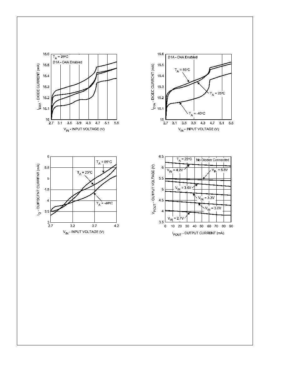
Typical Performance Characteristics
Unless otherwise specified: V
IN
= 3.6V; V
LEDxA
= 3.6V; V
LEDxB
= 3.6V; ENA = V
IN
and ENB = GND, or ENA = GND and ENB = V
IN
; R
SETA
= R
SETB
= 8.35k
; C
IN
, C
1
, C
2
, and C
POUT
=
1µF.
LED Current (D1A, D2A,D3A, D4A)
vs. Input Voltage
LED Current (DxA) vs. Input Voltage
20127904
20127905
Quiescent Current vs. Input Voltage,
Charge Pump Output Voltage
vs. Output Current
20127906
20127907
LM27961
www.national.com
5