LM27964
White LED Driver System with I2C Compatible
Brightness Control
General Description
The LM27964 is a charge-pump-based white-LED driver that
is ideal for mobile phone display backlighting. The LM27964
can drive up to 6 LEDs in parallel along with multiple keypad
LEDs, with a total output current up to 180mA. Regulated
internal current sources deliver excellent current matching in
all LEDs.
The LED driver current sources are split into two indepen-
dently controlled groups. The primary group (4 LEDs) can be
used to backlight the main phone display and the second
group (2 LEDs) can be used to backlight a secondary dis-
play. A single Keypad LED driver can power up to 16 keypad
LEDs with a current of 5mA each. The LM27964 has an I
2
C
compatible interface that allows the user to independently
control the brightness on each bank of LEDs.
The LM27964 works off an extended Li-Ion input voltage
range (2.7V to 5.5V). The device provides excellent effi-
ciency without the use of an inductor by operating the charge
pump in a gain of 3/2, or in Pass-Mode. The proper gain for
maintaining current regulation is chosen, based on LED
forward voltage, so that efficiency is maximized over the
input voltage range.
The LM27964 is available in National's small 24-pin Lead-
less Leadframe Package (LLP-24).
Features
n
87% Peak LED Drive Efficiency
n
0.2% Current Matching between Current Sinks
n
Drives 6 LEDs with up to 30mA per LED in two distinct
groups, for backlighting two displays (main LCD and sub
LCD)
n
Dedicated Keypad LED Driver with up to 80mA of drive
current
n
Independent Resistor-Programmable Current Settings
n
I
2
C Compatible Brightness Control Interface
n
Adaptive 1x- 3/2x Charge Pump
n
Extended Li-Ion Input: 2.7V to 5.5V
n
Small low profile industry standard leadless package,
LLP 24 : (4mm x 4mm x 0.8mm)
n
LM27964SQ-I LED PWM frequency = 10kHz,
LM27964SQ-A LED PWM frequency = 23kHz
Applications
n
Mobile Phone Display Lighting
n
Mobile Phone Keypad Lighting
n
PDAs Backlighting
n
General LED Lighting
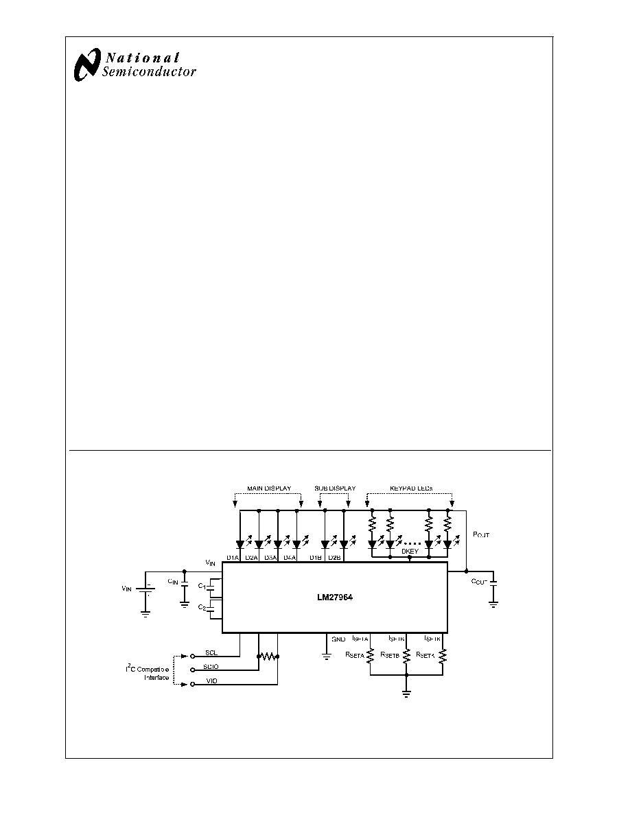
Typical Application Circuit
20138101
October 2005
LM27964
White
LED
Driver
System
with
I
2
C
Compatible
Brightness
Control
� 2005 National Semiconductor Corporation
DS201381
www.national.com
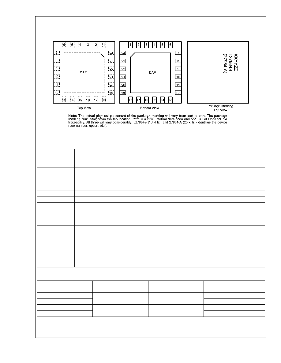
Connection Diagram
24 Pin Quad LLP Package
NS Package Number SQA24A
20138102
Pin Descriptions
Pin #s
Pin Names
Pin Descriptions
24
V
IN
Input voltage. Input range: 2.7V to 5.5V.
23
P
OUT
Charge Pump Output Voltage
19, 22 (C1)
20, 21 (C2)
C1, C2
Flying Capacitor Connections
13, 14, 15, 16
D4A, D3A, D2A,
D1A
LED Drivers - GroupA
4, 5
D1B, D2B
LED Drivers - GroupB
6
DKEY
LED Driver - KEYPAD
17
I
SETA
Placing a resistor (R
SETA
) between this pin and GND sets the full-scale LED
current for Group A LEDs. LED Current = 200 x (1.25V � R
SETA
)
3
I
SETB
Placing a resistor (R
SETB
) between this pin and GND sets the full-scale LED
current for Group B LEDs. LED Current = 200 x (1.25V � R
SETB
)
12
I
SETK
Placing a resistor (R
SETK
) between this pin and GND sets the total LED
current for the KEYPAD LEDs. Keypad LED Current = 800 x (1.25V � R
SETK
)
1
SCL
Serial Clock Pin
2
SDIO
Serial Data Input/Output Pin
7
VIO
Serial Bus Voltage Level Pin
9, 10, 18, DAP
GND
Ground
8, 11
NC
No Connect
Ordering Information
Order Information
Current Source
PWM Frequency
Package
Supplied As
LM27964SQ-I
10kHz.
SQA24 LLP
1000 Units, Tape & Reel
LM27964SQX-I
4500 Units, Tape & Reel
LM27964SQ-A
23kHz.
SQA24 LLP
1000 Units, Tape & Reel
LM27964SQX-A
4500 Units, Tape & Reel
LM27964
www.national.com
2
Absolute Maximum Ratings
(Notes 1, 2)
If Military/Aerospace specified devices are required,
please contact the National Semiconductor Sales Office/
Distributors for availability and specifications.
V
IN
pin voltage
-0.3V to 6.0V
SCL, SDIO, VIO pin voltages
-0.3V to (V
IN
+0.3V)
w/ 6.0V max
I
Dxx
Pin Voltages
-0.3V to
(V
POUT
+0.3V)
w/ 6.0V max
Continuous Power Dissipation
(Note 3)
Internally Limited
Junction Temperature (T
J-MAX
)
150
o
C
Storage Temperature Range
-65
o
C to +150
o
C
Maximum Lead Temperature
(Soldering)
(Note 4)
ESD Rating (Note 5)
Human Body Model - I
Dxx
Pins:
Human Body Model - All other
Pins:
1.0kV
2.0kV
Operating Rating
(Notes 1, 2)
Input Voltage Range
2.7V to 5.5V
LED Voltage Range
2.0V to 4.0V
Junction Temperature (T
J
) Range
-30�C to +100�C
Ambient Temperature (T
A
)
Range(Note 6)
-30�C to +85�C
Thermal Properties
Juntion-to-Ambient Thermal
Resistance (
JA
), SQA24A Package
(Note 7)
41.3�C/W
Electrical Characteristics
(Notes 2, 8)
Limits in standard typeface are for T
J
= 25�C, and limits in boldface type apply over the full operating temperature range. Un-
less otherwise specified: V
IN
= 3.6V; V
DxA
= 0.4V; V
DxB
= 0.4V; V
DKEY
= 0.4V; R
SETA
= R
SETB
= R
SETK
= 16.9k
; BankA,
BankB, and DKEY = Fullscale Current; ENA, ENB, ENK Bits = "1"; C1=C2=1.0�F, C
IN
=C
OUT
=2.2�F; Specifications related to
output current(s) and current setting pins (I
Dxx
and I
SETx
) apply to BankA, BankB and DKEY. (Note 9)
Symbol
Parameter
Condition
Min
Typ
Max
Units
I
Dxx
Output Current Regulation
BankA or BankB Enabled
3.0V
V
IN
5.5V
BankA or BankB Full-Scale
ENA or ENB = "1", ENK = "0"
13.77
(-10%)
15.3
16.83
(+10%)
mA
(%)
3.0V
V
IN
5.5V
BankA or BankB Half-Scale
ENA or ENB = "1", ENK = "0"
7.5
mA
2.7V
V
IN
3.0V
BankA or BankB Full-Scale
ENA or ENB = "1", ENK = "0"
15
mA
Output Current Regulation
Keypad Driver Enabled
3.0V
V
IN
5.5V
DKEY Full-Scale
ENA = ENB = "0", ENK = "1"
52.8
(-12%)
60
67.2
(+12%)
mA
(%)
Output Current Regulation
BankA and DKEY Enabled
(Note 10)
3.2V
V
IN
5.5V
R
SETA
= 8.3k
, R
SETK
= 16.9k
V
LED
= 3.6V
BankA and DKEY Full-Scale
ENA = ENK = "1", ENB = "0"
30
DxA
mA
60
DKEY
R
OUT
Open-Loop Charge Pump Output
Resistance
Gain = 3/2
2.75
Gain = 1
1
V
DxTH
V
Dxx
1x to 3/2x Gain Transition
Threshold
V
DxA
and/or V
DxB
Falling
375
mV
LM27964
www.national.com
3

Electrical Characteristics
(Notes 2, 8) (Continued)
Limits in standard typeface are for T
J
= 25�C, and limits in boldface type apply over the full operating temperature range. Un-
less otherwise specified: V
IN
= 3.6V; V
DxA
= 0.4V; V
DxB
= 0.4V; V
DKEY
= 0.4V; R
SETA
= R
SETB
= R
SETK
= 16.9k
; BankA,
BankB, and DKEY = Fullscale Current; ENA, ENB, ENK Bits = "1"; C1=C2=1.0�F, C
IN
=C
OUT
=2.2�F; Specifications related to
output current(s) and current setting pins (I
Dxx
and I
SETx
) apply to BankA, BankB and DKEY. (Note 9)
Symbol
Parameter
Condition
Min
Typ
Max
Units
V
HR
Current Source Headroom Voltage
Requirement
(Note 11)
I
Dxx
= 95% xI
Dxx
(nom.)
(I
Dxx
(nom)
15mA)
BankA and/or BankB Full-Scale
Gain = 3/2, ENA and/or ENB = "1"
180
mV
I
DKEY
= 95% xI
DKEY
(nom.)
(I
DKEY
(nom)
60mA)
DKEY Full-Scale
Gain = 3/2, ENK = "1"
180
I
Dxx-MATCH
LED Current Matching
(Note 12)
0.2
2
%
I
Q
Quiescent Supply Current
Gain = 1.5x, No Load
1.3
1.7
mA
I
SD
Shutdown Supply Current
All ENx bits = "0"
3.0
5
�A
V
SET
I
SET
Pin Voltage
2.7V
V
IN
5.5V
1.25
V
I
DxA-B /
I
SETA-B
Output Current to Current Set
Ratio BankA and BankB
200
I
DKEY
/
I
SETK
Output Current to Current Set
Ratio DKEY
800
f
SW
Switching Frequency
500
700
900
kHz
t
START
Start-up Time
P
OUT
= 90% steady state
250
�s
f
PWM
Internal Diode Current PWM
Frequency
LM27964SQ-I
10
kHz
LM27964SQ-A
23
D.C. Step Diode Current Duty Cycle Step
1/16
Fullscale
I
2
C Compatible Interface Voltage Specifications (SCL, SDIO, VIO)
V
IO
Serial Bus Voltage Level
1.8
V
IN
V
V
IL
Input Logic Low "0"
2.7V
V
IN
5.5V
0
0.27 x
V
IO
V
V
IH
Input Logic High "1"
2.7V
V
IN
5.5V
0.73 x
V
IO
V
IO
V
V
OL
Output Logic Low "0"
I
LOAD
= 2mA
400
mV
I
2
C Compatible Interface Timing Specifications (SCL, SDIO, VIO)(Note 13)
t
1
SCL (Clock Period)
2.5
�s
t
2
Data In Setup Time to SCL High
100
ns
t
3
Data Out stable After SCL Low
0
ns
t
4
SDIO Low Setup Time to SCL Low
(Start)
100
ns
t
5
SDIO High Hold Time After SCL
High (Stop)
100
ns
20138113
LM27964
www.national.com
4
Electrical Characteristics
(Notes 2, 8) (Continued)
Note 1: Absolute Maximum Ratings indicate limits beyond which damage to the component may occur. Operating Ratings are conditions under which operation of
the device is guaranteed. Operating Ratings do not imply guaranteed performance limits. For guaranteed performance limits and associated test conditions, see the
Electrical Characteristics tables.
Note 2: All voltages are with respect to the potential at the GND pin.
Note 3: Internal thermal shutdown circuitry protects the device from permanent damage. Thermal shutdown engages at T
J
= 170�C (typ.) and disengages at T
J
=
165�C (typ.).
Note 4: For detailed soldering specifications and information, please refer to National Semiconductor Application Note 1187: Leadless Leadframe Package
(AN-1187).
Note 5: The Human body model is a 100pF capacitor discharged through a 1.5k
resistor into each pin. MIL-STD-883 3015.7
Note 6: In applications where high power dissipation and/or poor package thermal resistance is present, the maximum ambient temperature may have to be
derated. Maximum ambient temperature (T
A-MAX
) is dependent on the maximum operating junction temperature (T
J-MAX-OP
= 100�C), the maximum power
dissipation of the device in the application (P
D-MAX
), and the junction-to ambient thermal resistance of the part/package in the application (
JA
), as given by the
following equation: T
A-MAX
= T
J-MAX-OP
� (
JA
x P
D-MAX
).
Note 7: Junction-to-ambient thermal resistance is highly dependent on application and board layout. In applications where high maximum power dissipation exists,
special care must be paid to thermal dissipation issues in board design. For more information, please refer to National Semiconductor Application Note 1187:
Leadless Leadframe Package (AN-1187).
Note 8: Min and Max limits are guaranteed by design, test, or statistical analysis. Typical numbers are not guaranteed, but do represent the most likely norm.
Note 9: C
IN
, C
POUT
, C
1
, and C
2
: Low-ESR Surface-Mount Ceramic Capacitors (MLCCs) used in setting electrical characteristics
Note 10: The maximum total output current for the LM27964 should be limited to 180mA. The total output current can be split among any of the three banks (I
DxA
= I
DxB
= 30mA Max., I
DKEY
= 80mA Max.). Under maximum output current conditions, special attention must be given to input voltage and LED forward voltage to
ensure proper current regulation. See the Maximum Output Current section of the datasheet for more information.
Note 11: For each I
Dxx
output pin, headroom voltage is the voltage across the internal current sink connected to that pin. For Group A and B outputs, V
HR
= V
OUT
-V
Dxx
. If headroom voltage requirement is not met, LED current regulation will be compromised.
Note 12: For the two groups of outputs on a part (BankA and BankB), the following are determined: the maximum output current in the group (MAX), the minimum
output current in the group (MIN), and the average output current of the group (AVG). For each group, two matching numbers are calculated: (MAX-AVG)/AVG and
(AVG-MIN)/AVG. The largest number of the two (worst case) is considered the matching figure for the bank. The matching figure for a given part is considered to
be the highest matching figure of the two banks. The typical specification provided is the most likely norm of the matching figure for all parts.
Note 13: SCL and SDIO should be glitch-free in order for proper brightness control to be realized.
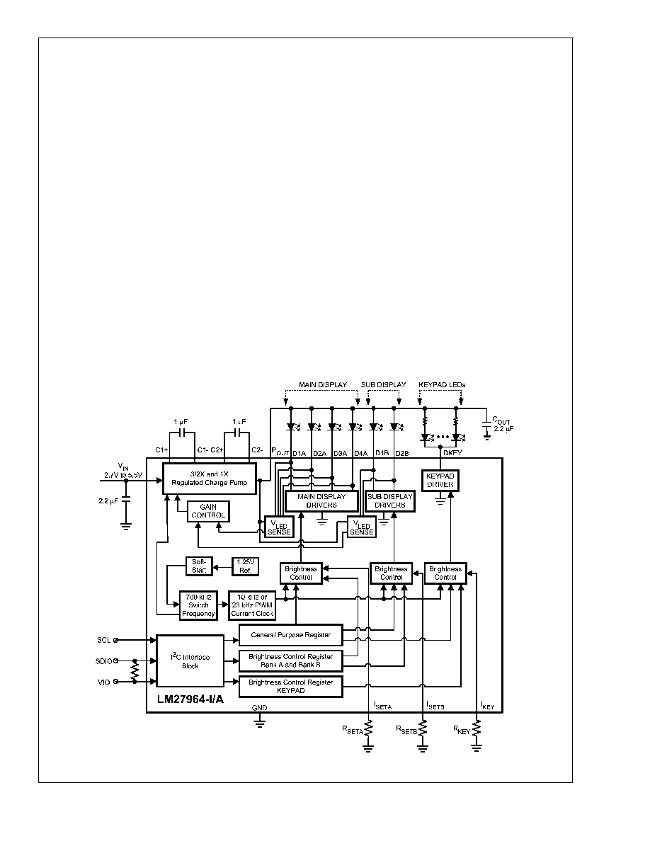
Block Diagram
20138103
LM27964
www.national.com
5