LM2797/LM2798
120mA High Efficiency Step-Down Switched Capacitor
Voltage Converter with Voltage Monitoring
General Description
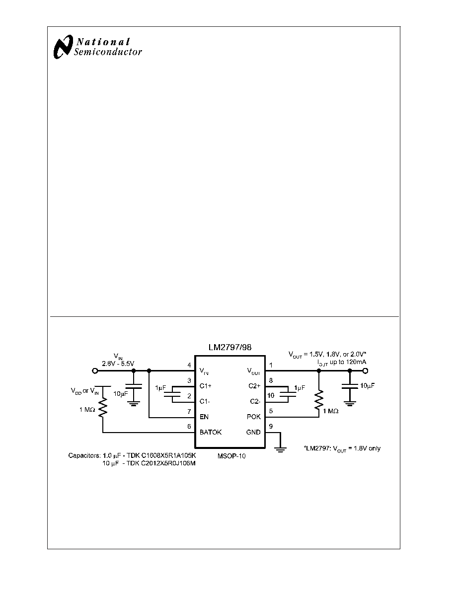
The LM2797/98 switched capacitor step-down DC/DC con-
verters efficiently produce a 120mA regulated low-voltage
rail from a 2.6V to 5.5V input. Fixed output voltage options of
1.5V, 1.8V, and 2.0V are available. The LM2797/98 uses
multiple fractional gain configurations to maximize conver-
sion efficiency over the entire input voltage and output cur-
rent ranges. Also contributing to high overall efficiency is the
extremely low supply current of the LM2797/98: 35µA oper-
ating unloaded and 0.1µA in shutdown.
Features of the LM2797/98 include input voltage and output
voltage monitoring. Pin BATOK provides battery monitoring
by indicating when the input voltage is above 2.85V (typ.).
Pin POK verifies that the output voltage is not more than 5%
(typ.) below the nominal output voltage of the part.
The optimal external component requirements of the
LM2797/98 solution minimize size and cost, making the part
ideal for Li-Ion and other battery powered designs. Two 1µF
flying capacitors and two 10µF bypass capacitors are all that
is required, and no inductors are needed.
The LM2797/98 also features short-circuit protection over-
temperature protection, and soft-start circuitry to prevent
excessive inrush currents. The LM2798 has a 400µs turn-on
time. The turn-on time of the LM2797 is 100µs.
Features
n
Output voltage options:
2.0V
±
5%, 1.8V
±
5%, and 1.5V
±
6%
n
120mA output current capability
n
Multi-Gain and Gain Hopping for Highest Possible
Efficiency - up to 90% Efficient
n
2.6V to 5.5V input range
n
Input and Output Voltage Monitoring (BATOK and POK)
n
Low operating supply current: 35µA
n
Shutdown supply current: 0.1µA
n
Thermal and short circuit protection
n
LM2798 turn-on time: 400µs
LM2797 turn-on time: 100µs
n
Available in an 10-Pin MSOP Package
Applications
n
Cellular Phones
n
Pagers
n
H/PC and P/PC Devices
n
Portable Electronic Equipment
n
Handheld Instrumentation
Typical Application Circuit
20044501
April 2003
LM2797/LM2798
120mA
High
Efficiency
Step-Down
Switched
Capacitor
V
oltage
Converter
with
V
oltage
Monitoring
© 2003 National Semiconductor Corporation
DS200445
www.national.com
Connection Diagram
LM2797/98
Mini SO-10 (MSOP-10) Package
NS Package #: MUB10A
20044502
Top View
Pin Description
Pin
Name
Description
1
V
OUT
Regulated Output Voltage
2
C1-
First Flying Capacitor: Negative Terminal
3
C1+
First Flying Capicitor: Positive terminal
4
V
IN
Input Voltage. Recommended V
IN
Range: 2.6V to 5.5V
5
POK
Power-OK Indicator: Output voltage sense. Open-drain NFET output. With an
external pull-up resistor tied to POK, V(POK) will be high when V
OUT
is
regulating correctly. When V
OUT
falls out of regulation, the internal open-drain
FET pulls the POK voltage low.
6
BATOK
Battery-OK Indicator: Input voltage sense. Open-drain NFET output. With an
external pull-up resistor tied to BATOK, V(BATOK) will be high when V
IN
>
2.85V (typ). LM2797/98 pulls V(BATOK) low when V
IN
<
2.65V (typ.) , and/or
when the part is in shutdown [V(EN) = 0].
7
EN
Enable Logic Input. High voltage = ON, Low voltage = SHUTDOWN
8
C2+
Second Flying Capacitor: Positive Terminal
9
GND
Ground Connection
10
C2-
Second Flying Capacitor: Negative Terminal
Ordering Information
Nominal
Output
Voltage
V
OUT(NOM)
Turn-on
Time
Order Number
Package Marking
Supplied As:
1.80V
100µs
LM2797MM-1.8
S80B
1000 units on Tape-and Reel
LM2797MMX-1.8
3500 units on Tape-and-Reel
1.50V
400µs
LM2798MM-1.5
S56B
1000 units on Tape-and Reel
LM2798MMX-1.5
3500 units on Tape-and-Reel
1.80V
400µs
LM2798MM-1.8
S57B
1000 units on Tape-and Reel
LM2798MMX-1.8
3500 units on Tape-and-Reel
2.00V
400µs
LM2798MM-2.0
S58B
1000 units on Tape-and Reel
LM2798MMX-2.0
3500 units on Tape-and-Reel
LM2797/LM2798
www.national.com
2
Absolute Maximum Ratings
(Notes 1,
2)
If Military/Aerospace specified devices are required,
please contact the National Semiconductor Sales Office/
Distributors for availability and specifications.
V
IN
, EN, POK, BATOK pins: Voltage
to Ground (Note 3)
-0.3V to 5.6V
Junction Temperature (T
J-MAX-ABS
)
150∞C
Continuous Power Dissipation
(Note 4)
Internally Limited
V
OUT
Short-Circuit to GND Duration
(Note 4)
Unlimited
Storage Temperature Range
-65∞C to 150∞C
Lead Temperature
(Soldering, 5 Sec.)
260∞C
ESD Rating (Note 5)
Human-body model:
Machine model
2 kV
200V
Operating Ratings
(Notes 1, 2)
Input Voltage Range
2.6V to 5.5V
Recommended Output Current
Range
0mA to 120mA
Junction Temperature Range
-40∞C to 125∞C
Ambient Temperature Range
(Note 6)
-40∞C to 85∞C
Thermal Information
Thermal Resistance, MSOP-8
220∞C/W
Resistance, MSOP-8 Package
(
JA
) (Note 7)
Electrical Characteristics
(Notes 2, 8)
Limits in standard typeface and typical values apply for T
J
= 25
o
C. Limits in boldface type apply over the operating junction
temperature range. Unless otherwise specified: 2.6
V
IN
5.5V, V(EN) = V
IN
, C
1
= C
2
= 1µF, C
IN
= C
OUT
= 10µF. (Note 9)
Symbol
Parameter
Conditions
Min
Typ
Max
Units
LM2797-1.8, LM2798-1.8, LM2798-2.0
V
OUT
Output Voltage Tolerance
2.8V
V
IN
4.2V
0mA
I
OUT
120mA
-5
+5
% of
V
OUT(nom)
(Note 10)
4.2V
<
V
IN
5.5V
0mA
I
OUT
120mA
-6
+6
LM2798-1.5
V
OUT
Output Voltage Tolerance
2.8V
V
IN
4.2V
0mA
I
OUT
120mA
-6
+6
% of
V
OUT(nom)
(Note 10)
4.2V
<
V
IN
5.5V
0mA
I
OUT
120mA
-6
+6
All Output Voltage Options
I
Q
Operating Supply Current
I
OUT
= 0mA
35
50
µA
I
SD
Shutdown Supply Current
V(EN) = 0V
0.1
2
µA
V
R
Output Voltage Ripple
LM2798-1.8: V
IN
= 3.6V, I
OUT
= 120mA
20
mV
p-p
E
PEAK
Peak Efficiency
LM2798-1.8: V
IN
= 3.0V, I
OUT
= 60mA
90
%
E
AVG
Average Efficiency over
Li-Ion Input Voltage Range
(Note 11)
LM2798-1.5: 3.0
V
IN
4.2V, I
OUT
= 60mA
76
%
LM2798-1.8: 3.0
V
IN
4.2V, I
OUT
= 60mA
82
LM2798-2.0: 3.0
V
IN
4.2V, I
OUT
= 60mA
75
t
ON
Turn-On Time
LM2798, V
IN
=2.6V, I
OUT
=100mA, (Note 12)
400
µs
LM2797, V
IN
=2.6V, I
OUT
=100mA, (Note 12)
100
f
SW
Switching Frequency
500
kHz
I
SC
Short-Circuit Current
V
IN
= 3.6, V
OUT
= 0V
25
mA
Enable Pin (EN) Characteristics
V
IH
EN pin Logic-High Input
0.9
V
IN
V
V
IL
EN pin Logic-Low Input
0
0.4
V
I
EN
EN pin input current
V
EN
= 0V
0
nA
V
EN
= 5.5V
30
LM2797/LM2798
www.national.com
3
Electrical Characteristics
(Notes 2, 8)
(Continued)
Limits in standard typeface and typical values apply for T
J
= 25
o
C. Limits in boldface type apply over the operating junction
temperature range. Unless otherwise specified: 2.6
V
IN
5.5V, V(EN) = V
IN
, C
1
= C
2
= 1µF, C
IN
= C
OUT
= 10µF. (Note 9)
Symbol
Parameter
Conditions
Min
Typ
Max
Units
POK Characteristics
V
T-POK
Threshold of output voltage
for POK transition
POK transition L to H
95
99
% of
V
OUT-NOM
(Note 10)
POK transition H to L
83
92
Hysterisis
3
I
POK-H
POK-high leakage current
V(POK) = 3.6V
1
5
µA
V
POK-L
POL-low pull-down voltage
I(POK) = -100µA
200
300
mV
BATOK Characteristics
V
T-BATOK
Input voltage threshold for
BATOK transition
BATOK transition L to H
2.85
3.0
V
BATOK transition H to L
2.4
2.65
Hysterisis
0.20
I
BATOK-H
BATOK-high leakage
current
V(BATOK) = 3.6V
1
5
µA
V
BATOK-L
BATOK-low pull-down
voltage
I(BATOK) = - 100µA
200
300
mV
Note 1: Absolute Maximum Ratings indicate limits beyond which damage to the component may occur. Operating Ratings are conditions under which operation of
the device is guaranteed. Operating Ratings do not imply guaranteed performance limits. For guaranteed performance limits and associated test conditions, see the
Electrical Characteristics tables.
Note 2: All voltages are with respect to the potential at the GND pin.
Note 3: Voltage on the EN pin must not be brought above V
IN
+ 0.3V.
Note 4: Thermal shutdown circuitry protects the device from permanent damage.
Note 5: The human-body model is a 100 pF capacitor discharged through a 1.5k
resistor into each pin. The machine model is a 200pF capacitor discharged
directly into each pin.
Note 6: Maximum ambient temperature (T
A-MAX
) is dependent on the maximum operating junction temperature (T
J-MAX-OP
= 125
o
C), the maximum power
dissipation of the device in the application (P
D-MAX
), and the junction-to ambient thermal resistance of the part/package in the application (
JA
), as given by the
following equation: T
A-MAX
= T
J-MAX-OP
- (
JA
x P
D-MAX
). The ambient temperature operating rating is provided merely for convenience. This part may be operated
outside the listed T
A
rating so long as the junction temperature of the device does not exceed the maximum operating rating of 125
o
C.
Note 7: Junction-to-ambient thermal resistance is highly dependent on application conditions and PC board layout. In applications where high maximum power
dissipation exists, special care must be paid to thermal dissipation issues. For more information on these topics, please refer to the Power Dissipation section of
this datasheet.
Note 8: All room temperature limits are 100% tested or guaranteed through statistical analysis. All limits at temperature extremes are guaranteed by correlation
using standard Statistical Quality Control methods (SQC). All limits are used to calculate Average Outgoing Quality Level (AOQL). Typical numbers are not
guaranteed, but do represent the most likely norm.
Note 9: C
IN
, C
OUT
, C
1
, and C
2
: Low-ESR Surface-Mount Ceramic Capacitors (MLCCs) used in setting electrical characteristics
Note 10: V
OUT (NOM)
is the nominal output voltage of the part. An example: V
OUT-NOM
of LM2798MM-1.8 is 1.8V.
Note 11: Efficiency is measured versus V
IN
, with V
IN
being swept in small increments from 3.0V to 4.2V. The average is calculated from these measurement results.
Weighting to account for battery voltage discharge characteristics (V
BAT
vs. Time) is not done in computing the average.
Note 12: Turn-on time is measured from when the EN signal is pulled high until the output voltage crosses 90% of its final value. Resistive load used for startup
measurement, with value chosen to give I
OUT
= 100mA when the output voltage is fully established.
LM2797/LM2798
www.national.com
4
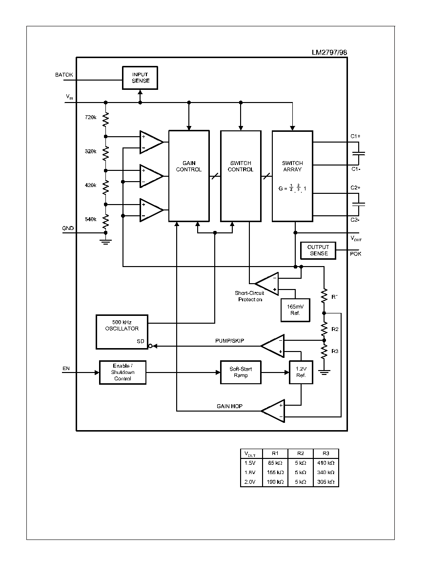
Block Diagram
20044503
LM2797/LM2798
www.national.com
5