Äîêóìåíòàöèÿ è îïèñàíèÿ www.docs.chipfind.ru
LM27
SOT-23,
±
3°C Accurate, 120°C-150°C Factory Preset
Thermostat
General Description
The LM27 is a precision, single digital-output, low-power
thermostat comprised of an internal reference, DAC, tem-
perature sensor and comparator. Utilizing factory program-
ming, it can be manufactured with different trip points as well
as different digital output functionality. The trip point (T
OS
)
can be preset at the factory to any temperature in the range
of +120°C to +150°C in 1°C increments. The LM27 has one
digital output (OS/OS/US/US), one digital input (HYST) and
one analog output (V
TEMP
). The digital output stage can be
preset as either open-drain or push-pull. In addition, it can be
factory programmed to be active HIGH or LOW. The digital
output can be factory programmed to indicate an over tem-
perature shutdown event (OS or OS) or an under tempera-
ture shutdown event (US or US). When preset as an over-
temperature shutdown (OS) it will go LOW to indicate that
the die temperature is over the internally preset T
OS
and go
HIGH when the temperature goes below (T
OS
T
HYST
). Simi-
larly, when preprogrammed as an undertemperature shut-
down (US) it will go HIGH to indicate that the temperature is
below T
US
and go LOW when the temperature is above
(T
US
+T
HYST
). The typical hysteresis, T
HYST
, can be set to
2°C or 10°C and is controlled by the state of the HYST pin. A
V
TEMP
analog output provides a voltage that is proportional
to temperature and has a -10.7mV/°C output slope.
Currently, there are several standard parts available, see
ordering information for details. For other part options, con-
tact a National Semiconductor Distributor or Sales Repre-
sentative for information on minimum order qualification. The
LM27 is currently available in a 5-lead SOT-23 package.
Applications
n
Microprocessor Thermal Management
n
Appliances
n
Portable Battery Powered Systems
n
Fan Control
n
Industrial Process Control
n
HVAC Systems
n
Electronic System Protection
Features
n
Internal comparator with pin selectable 2°C or 10°C
hysteresis
n
No external components required
n
Open-drain or push-pull digital output; supports CMOS
logic levels
n
Internal temperature sensor with V
TEMP
output pin
n
V
TEMP
output allows after-assembly system testing
n
Internal voltage reference and DAC for trip-point setting
n
Currently available in 5-pin SOT-23 plastic package
n
Excellent power supply noise rejection
Key Specifications
j
Power Supply Voltage
2.7V to 5.5V
j
Power Supply Current
40µA(max)
15µA(typ)
j
Hysteresis Temperature
2°C or 10°C(typ)
j
Temperature Trip Point Accuracy
±
3°C (max)
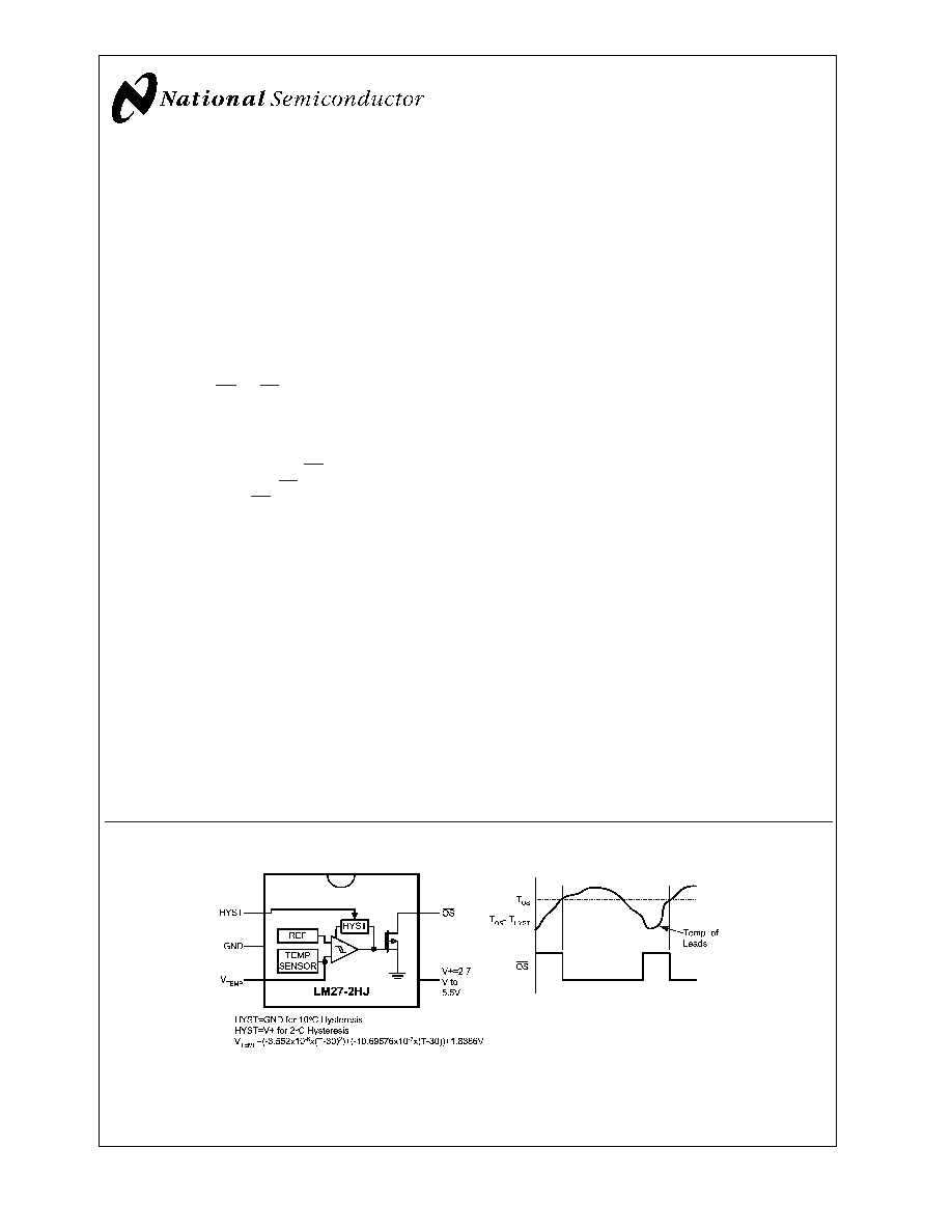
LM27CIM5-2HJ Simplified Block Diagram and Connection Diagram
20030701
The LM27CIM5-2HJ has a fixed trip point of 140°C.
For other trip point and output function availability,
please see ordering information or contact National Semiconductor.
August 2002
LM27
SOT
-23,
±
3°C
Accurate,
120°C-150°C
Factory
Preset
Thermostat
© 2002 National Semiconductor Corporation
DS200307
www.national.com
Ordering Information
For more detailed information on the suffix meaning see the part number template at the end of the Electrical Characteris-
tics Section. Contact National Semiconductor for other set points and output options.
Order Number
Top Mark
NS Package
Number
Trip Point Setting
Output Function
Bulk Rail
3000 Units in Tape & Reel
LM27CIM5-1HJ
LM27CIM5X-1HJ
T1HJ
MA05B
130°C
Open Drain OS
LM27CIM5-2HJ
LM27CIM5X-2HJ
T2HJ
MA05B
140°C
Open Drain OS
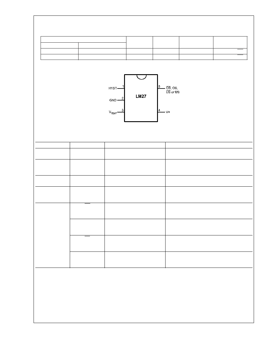
Connection Diagram
20030702
Pin Description
Pin Number
Pin Name
Function
Connection
1
HYST
Hysteresis control, digital
input
GND for 10°C or V
+
for 2°C
2
GND
Ground, connected to the
back side of the die through
lead frame.
System GND
3
V
TEMP
Analog output voltage
proportional to temperature
Leave floating or connect to a high impedance
node.
4
V
+
Supply input
2.7V to 5.5V with a 0.1µF bypass capacitor.
For PSRR information see Section Titled
NOISE CONSIDERATIONS.
5
OS
Overtemperature Shutdown
open-drain active low
thermostat digital output
Controller interrupt, system or power supply
shutdown; pull-up resistor
10k
OS
Overtemperature Shutdown
totem-pull active high
thermostat digital output
Controller interrupt, system or power supply
shutdown
US
Undertemperature Shutdown
open-drain active low
thermostat digital output
System or power supply shutdown; pull-up
resistor
10k
US
Undertemperature Shutdown
totem-pull active high
thermostat digital output
System or power supply shutdown
Note: pin 5 functionality and trip point setting are programmed during LM27 manufacture.
LM27
www.national.com
2

Absolute Maximum Ratings
(Note 1)
Input Voltage
6.0V
Input Current at any pin (Note 2)
5mA
Package Input Current(Note 2)
20mA
Package Dissipation at T
A
= 25°C
(Note 3)
500mW
Soldering Information
SOT23 Package
Vapor Phase (60 seconds)
Infrared (15 seconds)
215°C
220°C
Storage Temperature
-65°C to + 150°C
ESD Susceptibility (Note 4)
Human Body Model
Machine Model
2500V
250V
Operating Ratings
(Note 1)
Specified Temperature Range
T
MIN
T
A
T
MAX
LM27CIM
-40°C
T
A
+150°C
Positive Supply Voltage (V
+
)
+2.7V to +5.5V
Maximum V
OUT
+5.5V
LM27 Electrical Characteristics
The following specifications apply for V
+
= 2.7V
DC
to 5.5V
DC
, and V
TEMP
load current = 0µA unless otherwise specified. Bold-
face limits apply for T
A
= T
J
= T
MIN
to T
MAX
; all other limits T
A
= T
J
= 25°C unless otherwise specified.
Typical
LM27CIM
Units
Symbol
Parameter
Conditions
(Note 6)
Limits
(Limits)
(Note 7)
Temperature Sensor
Trip Point Accuracy (Includes
V
REF
, DAC, Comparator Offset,
and Temperature Sensitivity
errors)
+120°C
<
T
A
<
+150°C
±
3
°C (max)
Trip Point Hysteresis
HYST = GND
10
°C
HYST = V
+
2
°C
V
TEMP
Output Temperature
Sensitivity
-10.82
mV/°C
V
TEMP
Temperature Sensitivity
Error to Equation:
V
O
= (-3.552x10
-6
x(T-30)
2
+
(-10.695x10
-3
x(T-30))+
1.8386V
-30°C
T
A
150°C,
2.7V
V
+
5.5V
±
3
°C (max)
-55°C
T
A
150°C,
4.5V
V
+
5.5V
±
3
°C (max)
T
A
= 25°C
±
2.5
°C (max)
V
TEMP
Load Regulation
-1µA
I
L
0
0.070
mV
0
I
L
+40µA
0.7
mV (max)
V
TEMP
Line Regulation
+2.7V
V
+
+5.5V,
-30°C
T
A
+120°C
-0.2
mV/V
I
S
Supply Current
15
22
40
µA (max)
µA (max)
Digital Output and Input
I
OUT("1")
Logical "1" Output Leakage
Current (Note 9)
V
+
= +5.0V
0.001
1
µA (max)
V
OUT("0")
Logical "0" Output Voltage
I
OUT
= +1.2mA and
V
+
2.7V;
I
OUT
= +3.2mA and
V
+
4.5V; (Note 8)
0.4
V (max)
V
OUT("1")
Logical "1" Push-Pull Output
Voltage
I
SOURCE
= 500µA, V
+
2.7V
0.8 x V
+
V (min)
I
SOURCE
= 800µA,
V
+
4.5V
V
+
- 1.5
V (min)
V
IH
HYST Input Logical "1" Threshold
Voltage
0.8 x V
+
V (min)
V
IL
HYST Input Logical "0" Threshold
Voltage
0.2 x V
+
V (max)
LM27
www.national.com
3
Note 1: Absolute Maximum Ratings indicate limits beyond which damage to the device may occur. Operating Ratings indicate conditions for which the device is
functional, but do not guarantee specific performance limits. For guaranteed specifications and test conditions, see the Electrical Characteristics. The guaranteed
specifications apply only for the test conditions listed. Some performance characteristics may degrade when the device is not operated under the listed test
conditions.
Note 2: When the input voltage (V
I
) at any pin exceeds the power supply (V
I
<
GND or V
I
>
V
+
), the current at that pin should be limited to 5mA. The 20mA
maximum package input current rating limits the number of pins that can safely exceed the power supplies with an input current of 5mA to four. Under normal
operating conditions the maximum current that pins 2, 4 or 5 can handle is limited to 5mA each.
Note 3: The maximum power dissipation must be derated at elevated temperatures and is dictated by T
Jmax
(maximum junction temperature),
JA
(junction to
ambient thermal resistance) and T
A
(ambient temperature). The maximum allowable power dissipation at any temperature is P
D
= (T
Jmax
T
A
)/
JA
or the number
given in the Absolute Maximum Ratings, whichever is lower. For this device, T
Jmax
= 150°C. For this device the typical thermal resistance (
JA
) of the different
package types when board mounted follow:
Package Type
JA
SOT23-5, MA05B
250°C/W
Note 4: The human body model is a 100pF capacitor discharge through a 1.5k
resistor into each pin. The machine model is a 200pF capacitor discharged directly
into each pin.
Note 5: See the URL "http://www.national.com/packaging/" for other recommendations and methods of soldering surface mount devices.
Note 6: Typicals are at T
J
= T
A
= 25°C and represent most likely parametric norm.
Note 7: Limits are guaranteed to National's AOQL (Average Outgoing Quality Level).
Note 8: Care should be taken to include the effects of self heating when setting the maximum output load current. The power dissipation of the LM27 would increase
by 1.28mW when I
OUT
=3.2mA and V
OUT
=0.4V. With a thermal resistance of 250°C/W, this power dissipation would cause an increase in the die temperature of
about 0.32°C due to self heating. Self heating is not included in the trip point accuracy specification.
Note 9: The 1µA limit is based on a testing limitation and does not reflect the actual performance of the part. Expect to see a doubling of the current for every 15°C
increase in temperature. For example, the 1nA typical current at 25°C would increase to 16nA at 85°C.
Part Number Template
The series of digits labeled xyz in the part number LM27CIM-xyz, describe the set point value and the function of the output as
follows:
The place holders xy describe the set point temperature as shown in the following table.
x (10x)
y (1x)
Temperature (°C)
-
H
0
-
J
1
-
K
2
-
L
3
-
N
4
-
P
5
-
R
6
x (10x)
y (1x)
Temperature (°C)
-
S
7
-
T
8
-
V
9
Z
-
12
1
-
13
2
-
14
3
-
15
The value of z describes the assignment/function of the output as shown in the following table:
Active-Low/High
Open-Drain/
Push-Pull
OS/US
Value of z
Digital Output Function
0
0
0
J
Active-Low, Open-Drain, OS output
0
0
1
K
Active-Low, Open-Drain, US output
1
1
0
L
Active-High, Push-Pull, OS output
1
1
1
N
Active-High, Push-Pull, US output
For example:
·
the part number LM27CIM5-2SJ has T
OS
= 147°C, and programmed as an active-low open-drain overtemperature shutdown
output.
·
the part number LM27CIM5-ZLN has T
US
= 123°C, and programmed as an active-high, push-pull undertemperature shutdown
output.
Active-high open-drain and active-low push-pull options are available, please contact National Semiconductor for more informa-
tion.
LM27
www.national.com
4

Functional Description
LM27 OPTIONS
The LM27 can be factory programmed to have a trip point
anywhere in-between 120°C to 150°C.
Applications Hints
AFTER-ASSEMBLY PCB TESTING
The LM27's V
TEMP
output allows after-assembly PCB testing
by following a simple test procedure. Simply measuring the
V
TEMP
output voltage will verify that the LM27 has been
assembled properly and that its temperature sensing cir-
cuitry is functional. The V
TEMP
output has very weak drive
capability that can be overdriven by 1.5mA. Therefore, one
can simply force the V
TEMP
voltage to cause the digital
output to change state, thereby verifying that the comparator
and output circuitry function after assembly. Here is a
sample test procedure that can be used to test the
LM27CIM5X-2HJ which has a 140°C trip point.
1.
Turn on V
+
and measure V
TEMP
. Then calculate the
temperature reading of the LM27 using the equation:
V
O
= (-3.552x10
-6
x(T-30)
2
) +
(-10.69576x10
-3
x(T-30)) + 1.8386V
(1)
or
(2)
2.
Verify that the temperature measured in step one is
within (
±
3°C + error of reference temperature sensor) of
the ambient/board temperature. The ambient/board tem-
perature (reference temperature) should be measured
using an extremely accurate calibrated temperature sen-
sor, which is in close proximity to and mounted on the
same PCB as the LM27 perhaps even touching the GND
lead of the LM27 if possible. The LM27 will sence the
board temperature not the ambient temperature (see
Section Titled Mounting Considerations)
3.
A. Observe that OS is high.
B. Drive V
TEMP
to ground.
C. Observe that OS is now low.
D. Release the V
TEMP
pin.
E. Observe that OS is now high.
4.
A. Observe that OS is high.
B. Drive V
TEMP
voltage down gradually.
C. When OS goes low, note the V
TEMP
voltage.
D. V
TEMP
Trig = V
TEMP
at OS trigger (HIGH-
>
LOW)
E. Calculate Ttrig using Equation (2).
5.
A. Gradually raise V
TEMP
until OS goes HIGH. Note
V
TEMP
.
B. Calculate T
HYST
using Equation (2).
V
TEMP
LOADING
The V
TEMP
output has very weak drive capability (40µA
source, 1µA sink). So care should be taken when attaching
circuitry to this pin. Capacitive loading may cause the V
TEMP
output to oscillate. Simply adding a resistor in series as
shown in Figure 2 will prevent oscillations from occurring. To
determine the value of the resistor follow the guidelines
given in Table 1. The same value resistor will work for either
placement of the resistor. If an additional capacitive load is
placed directly on the LM27 output, rather than across
C
LOAD
, it should be at least a factor of 10 smaller than
C
LOAD
.
20030712
LM27-_ _J
20030713
LM27-_ _K
20030714
LM27-_ _L
20030715
LM27-_ _N
FIGURE 1. Output Pin Options Block Diagrams
LM27
www.national.com
5
Document Outline