 | –≠–ª–µ–∫—Ç—Ä–æ–Ω–Ω—ã–π –∫–æ–º–ø–æ–Ω–µ–Ω—Ç: LM2831XMF | –°–∫–∞—á–∞—Ç—å:  PDF PDF  ZIP ZIP |
LM2831
High Frequency 1.5A Load - Step-Down DC-DC
Regulator
General Description
The LM2831 regulator is a monolithic, high frequency, PWM
step-down DC/DC converter in a 5 pin SOT23 and a 6 Pin
LLP package. It provides all the active functions to provide
local DC/DC conversion with fast transient response and
accurate regulation in the smallest possible PCB area. With
a minimum of external components, the LM2831 is easy to
use. The ability to drive 1.5A loads with an internal 130 m
PMOS switch using state-of-the-art 0.5 µm BiCMOS technol-
ogy results in the best power density available. The world-
class control circuitry allows on-times as low as 30ns, thus
supporting exceptionally high frequency conversion over the
entire 3V to 5.5V input operating range down to the minimum
output voltage of 0.6V. Switching frequency is internally set
to 550 kHz, 1.6 MHz, or 3.0 MHz, allowing the use of
extremely small surface mount inductors and chip capaci-
tors. Even though the operating frequency is high, efficien-
cies up to 93% are easy to achieve. External shutdown is
included, featuring an ultra-low stand-by current of 30 nA.
The LM2831 utilizes current-mode control and internal com-
pensation to provide high-performance regulation over a
wide range of operating conditions. Additional features in-
clude internal soft-start circuitry to reduce inrush current,
pulse-by-pulse current limit, thermal shutdown, and output
over-voltage protection.
Features
n
Space Saving SOT23-5 Package
n
Input voltage range of 3.0V to 5.5V
n
Output voltage range of 0.6V to 4.5V
n
1.5A output current
n
High Switching Frequencies
1.6MHz (LM2831X)
0.55MHz (LM2831Y)
3.0MHz (LM2831Z)
n
130m
PMOS switch
n
0.6V, 2% Internal Voltage Reference
n
Internal soft-start
n
Current mode, PWM operation
n
Thermal Shutdown
n
Over voltage protection
Applications
n
Local 5V to Vcore Step-Down Converters
n
Core Power in HDDs
n
Set-Top Boxes
n
USB Powered Devices
n
DSL Modems
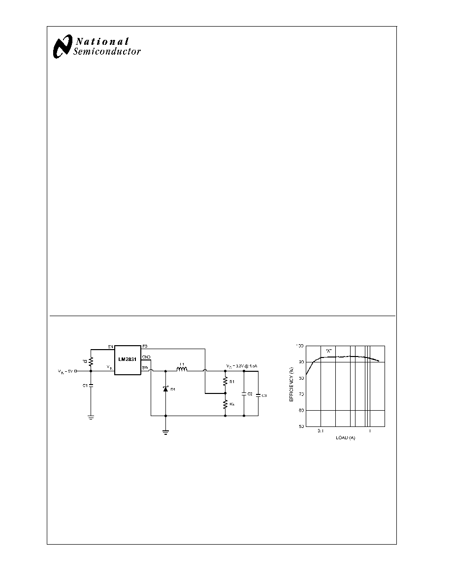
Typical Application Circuit
20174864
20174881
August 2006
LM2831
High
Frequency
1.5A
Load
-
Step-Down
DC-DC
Regulator
© 2006 National Semiconductor Corporation
DS201748
www.national.com
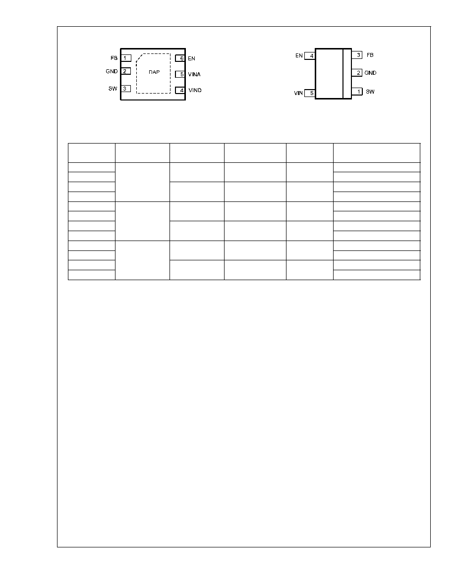
Connection Diagrams
20174801
6-Pin LLP
20174803
5-Pin SOT-23
Ordering Information
Order Number
Frequency
Option
Package Type
NSC Package
Drawing
Top Mark
Supplied As
LM2831XMF
1.6MHz
SOT23-5
MF05A
SKYB
1000 units Tape and Reel
LM2831XMFX
3000 units Tape and Reel
LM2831XSD
LLP-6
SDE06A
L193B
1000 units Tape and Reel
LM2831XSDX
4500 units Tape and Reel
LM2831YMF
0.55MHz
SOT23-5
MF05A
SKZB
1000 units Tape and Reel
LM2831YMFX
3000 units Tape and Reel
LM2831YSD
LLP-6
SDE06A
L194B
1000 units Tape and Reel
LM2831YSDX
4500 units Tape and Reel
LM2831ZMF
3MHz
SOT23-5
MF05A
SLAB
1000 units Tape and Reel
LM2831ZMFX
3000 units Tape and Reel
LM2831ZSD
LLP-6
SDE06A
L195B
1000 units Tape and Reel
LM2831ZSDX
4500 units Tape and Reel
NOPB versions available as well
LM2831
www.national.com
2
Pin Descriptions 5-Pin SOT23
Pin
Name
Function
1
SW
Output switch. Connect to the inductor and catch diode.
2
GND
Signal and power ground pin. Place the bottom resistor of the feedback network as close as
possible to this pin.
3
FB
Feedback pin. Connect to external resistor divider to set output voltage.
4
EN
Enable control input. Logic high enables operation. Do not allow this pin to float or be
greater than VIN + 0.3V.
5
VIN
Input supply voltage.
Pin Descriptions 6-Pin LLP
Pin
Name
Function
1
FB
Feedback pin. Connect to external resistor divider to set output voltage.
2
GND
Signal and power ground pin. Place the bottom resistor of the feedback network as
close as possible to this pin.
3
SW
Output switch. Connect to the inductor and catch diode.
4
VIND
Power Input supply.
5
VINA
Control circuitry supply voltage. Connect VINA to VIND on PC board.
6
EN
Enable control input. Logic high enables operation. Do not allow this pin to float or be
greater than VINA + 0.3V.
DAP
Die Attach Pad
Connect to system ground for low thermal impedance, but it cannot be used as a
primary GND connection.
LM2831
www.national.com
3
Absolute Maximum Ratings
(Note 1)
If Military/Aerospace specified devices are required,
please contact the National Semiconductor Sales Office/
Distributors for availability and specifications.
VIN
-0.5V to 7V
FB Voltage
-0.5V to 3V
EN Voltage
-0.5V to 7V
SW Voltage
-0.5V to 7V
ESD Susceptibility
2kV
Junction Temperature (Note 2)
150∞C
Storage Temperature
-65∞C to +150∞C
Soldering Information
Infrared or Convection Reflow
(15 sec)
220∞C
Operating Ratings
VIN
3V to 5.5V
Junction Temperature
-40∞C to +125∞C
Electrical Characteristics
VIN = 5V unless otherwise indicated under the Conditions column. Limits in
standard type are for T
J
= 25∞C only; limits in boldface type apply over the junction temperature (T
J
) range of -40∞C to
+125∞C. Minimum and Maximum limits are guaranteed through test, design, or statistical correlation. Typical values represent
the most likely parametric norm at T
J
= 25∞C, and are provided for reference purposes only.
Symbol
Parameter
Conditions
Min
Typ
Max
Units
V
FB
Feedback Voltage
LLP-6 and SOT23-5
Package
0.588
0.600
0.612
V
V
FB
/V
IN
Feedback Voltage Line Regulation
V
IN
= 3V to 5V
0.02
%/V
I
B
Feedback Input Bias Current
0.1
100
nA
UVLO
Undervoltage Lockout
V
IN
Rising
2.73
2.90
V
V
IN
Falling
1.85
2.3
UVLO Hysteresis
0.43
V
F
SW
Switching Frequency
LM2831-X
1.2
1.6
1.95
MHz
LM2831-Y
0.4
0.55
0.7
LM2831-Z
2.25
3.0
3.75
D
MAX
Maximum Duty Cycle
LM2831-X
86
94
%
LM2831-Y
90
96
LM2831-Z
82
90
D
MIN
Minimum Duty Cycle
LM2831-X
5
%
LM2831-Y
2
LM2831-Z
7
R
DS(ON)
Switch On Resistance
LLP-6 Package
150
m
SOT23-5 Package
130
195
I
CL
Switch Current Limit
V
IN
= 3.3V
1.8
2.5
A
V
EN_TH
Shutdown Threshold Voltage
0.4
V
Enable Threshold Voltage
1.8
I
SW
Switch Leakage
100
nA
I
EN
Enable Pin Current
Sink/Source
100
nA
I
Q
Quiescent Current (switching)
LM2831X V
FB
= 0.55
3.3
5
mA
LM2831Y V
FB
= 0.55
2.8
4.5
LM2831Z V
FB
= 0.55
4.3
6.5
Quiescent Current (shutdown)
All Options V
EN
= 0V
30
nA
LM2831
www.national.com
4
Electrical Characteristics
VIN = 5V unless otherwise indicated under the Conditions column. Limits in
standard type are for T
J
= 25∞C only; limits in boldface type apply over the junction temperature (T
J
) range of -40∞C to
+125∞C. Minimum and Maximum limits are guaranteed through test, design, or statistical correlation. Typical values represent
the most likely parametric norm at T
J
= 25∞C, and are provided for reference purposes only. (Continued)
Symbol
Parameter
Conditions
Min
Typ
Max
Units
JA
Junction to Ambient
0 LFPM Air Flow (Note 3)
LLP-6 Package
80
∞C/W
SOT23-5 Package
118
JC
Junction to Case (Note 3)
LLP-6 Package
18
∞C/W
SOT23-5 Package
80
T
SD
Thermal Shutdown Temperature
165
∞C
Note 1: Absolute maximum ratings indicate limits beyond which damage to the device may occur. Operating Range indicates conditions for which the device is
intended to be functional, but does not guarantee specfic performance limits. For guaranteed specifications and test conditions, see the Electrical Characteristics.
Note 2: Thermal shutdown will occur if the junction temperature exceeds the maximum junction temperature of the device.
Note 3: Applies for packages soldered directly onto a 3" x 3" PC board with 2oz. copper on 4 layers in still air.
LM2831
www.national.com
5