 | –≠–ª–µ–∫—Ç—Ä–æ–Ω–Ω—ã–π –∫–æ–º–ø–æ–Ω–µ–Ω—Ç: LM2832 | –°–∫–∞—á–∞—Ç—å:  PDF PDF  ZIP ZIP |
LM2832
High Frequency 2.0A Load - Step-Down DC-DC
Regulator
General Description
The LM2832 regulator is a monolithic, high frequency, PWM
step-down DC/DC converter in a 6 Pin LLP and a 8 Pin
eMSOP package. It provides all the active functions to pro-
vide local DC/DC conversion with fast transient response
and accurate regulation in the smallest possible PCB area.
With a minimum of external components, the LM2832 is
easy to use. The ability to drive 2.0A loads with an internal
150 m
PMOS switch using state-of-the-art 0.5 µm BiCMOS
technology results in the best power density available. The
world-class control circuitry allows on-times as low as 30ns,
thus supporting exceptionally high frequency conversion
over the entire 3V to 5.5V input operating range down to the
minimum output voltage of 0.6V. Switching frequency is
internally set to 550 kHz, 1.6 MHz, or 3.0 MHz, allowing the
use of extremely small surface mount inductors and chip
capacitors. Even though the operating frequency is high,
efficiencies up to 93% are easy to achieve. External shut-
down is included, featuring an ultra-low stand-by current of
30 nA. The LM2832 utilizes current-mode control and inter-
nal compensation to provide high-performance regulation
over a wide range of operating conditions. Additional fea-
tures include internal soft-start circuitry to reduce inrush
current, pulse-by-pulse current limit, thermal shutdown, and
output over-voltage protection.
Features
n
Input voltage range of 3.0V to 5.5V
n
Output voltage range of 0.6V to 4.5V
n
2.0A output current
n
High Switching Frequencies
1.6MHz (LM2832X)
0.55MHz (LM2832Y)
3.0MHz (LM2832Z)
n
150m
PMOS switch
n
0.6V, 2% Internal Voltage Reference
n
Internal soft-start
n
Current mode, PWM operation
n
Thermal Shutdown
n
Over voltage protection
Applications
n
Local 5V to Vcore Step-Down Converters
n
Core Power in HDDs
n
Set-Top Boxes
n
USB Powered Devices
n
DSL Modems
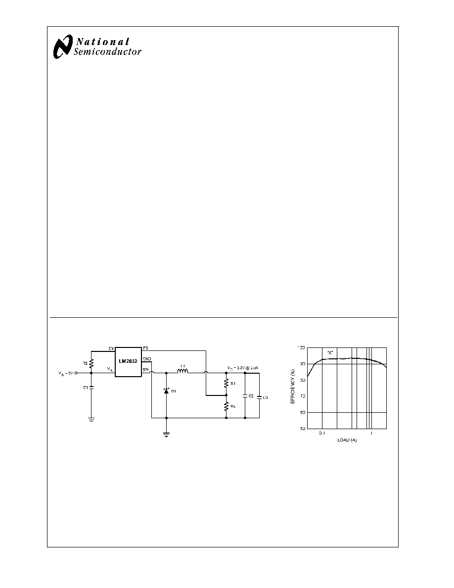
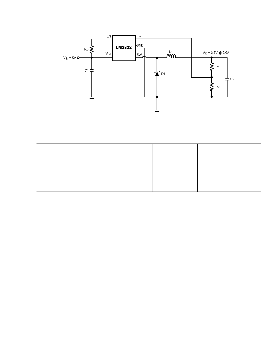
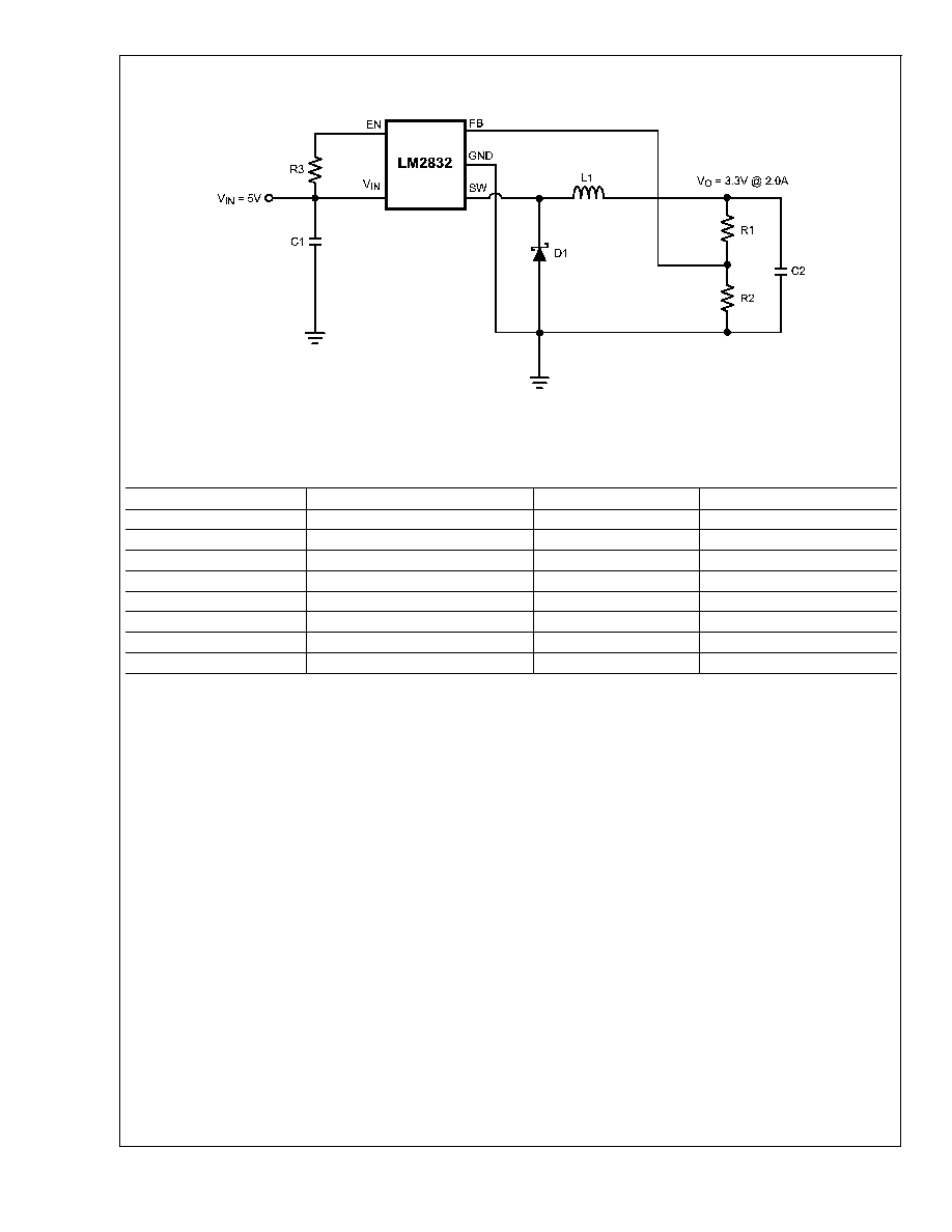
Typical Application Circuit
20197564
20197581
August 2006
LM2832
High
Frequency
2.0A
Load
-
Step-Down
DC-DC
Regulator
© 2006 National Semiconductor Corporation
DS201975
www.national.com

Connection Diagrams
20197501
6-Pin LLP
20197502
8-Pin eMSOP
Ordering Information
Order Number
Frequency
Option
Package Type
NSC Package
Drawing
Top Mark
Supplied As
LM2832XMY
1.6MHz
eMSOP-8
MUY08A
SLBB
1000 units Tape and Reel
LM2832XMYX
3500 units Tape and Reel
LM2832XSD
LLP-6
SDE06A
L196B
1000 units Tape and Reel
LM2832XSDX
4500 units Tape and Reel
LM2832YMY
0.55MHz
eMSOP-8
MUY08A
SLCB
1000 units Tape and Reel
LM2832YMYX
3500 units Tape and Reel
LM2832YSD
LLP-6
SDE06A
L197B
1000 units Tape and Reel
LM2832YSDX
4500 units Tape and Reel
LM2832ZMY
3MHz
eMSOP-8
MUY08A
SLDB
1000 units Tape and Reel
LM2832ZMYX
3500 units Tape and Reel
LM2832ZSD
LLP-6
SDE06A
L198B
1000 units Tape and Reel
LM2832ZSDX
4500 units Tape and Reel
NOPB versions available as well
LM2832
www.national.com
2

Pin Descriptions 8-Pin eMSOP
Pin
Name
Function
1
VIND
Power Input supply.
2
VINA
Control circuitry supply voltage. Connect VINA to VIND on PC board.
3, 5, 7
GND
Signal and power ground pin. Place the bottom resistor of the feedback network as close
as possible to this pin.
4
EN
Enable control input. Logic high enables operation. Do not allow this pin to float or be
greater
than VIN + 0.3V.
6
FB
Feedback pin. Connect to external resistor divider to set output voltage.
8
SW
Output switch. Connect to the inductor and catch diode.
DAP
Die Attach Pad
Connect to system ground for low thermal impedance, but it cannot be used as a primary
GND connection.
Pin Descriptions 6-Pin LLP
Pin
Name
Function
1
FB
Feedback pin. Connect to external resistor divider to set output voltage.
2
GND
Signal and power ground pin. Place the bottom resistor of the feedback network as
close as possible to this pin.
3
SW
Output switch. Connect to the inductor and catch diode.
4
VIND
Power Input supply.
5
VINA
Control circuitry supply voltage. Connect VINA to VIND on PC board.
6
EN
Enable control input. Logic high enables operation. Do not allow this pin to float or be
greater than VINA + 0.3V.
DAP
Die Attach Pad
Connect to system ground for low thermal impedance, but it cannot be used as a
primary GND connection.
LM2832
www.national.com
3
Absolute Maximum Ratings
(Note 1)
If Military/Aerospace specified devices are required,
please contact the National Semiconductor Sales Office/
Distributors for availability and specifications.
VIN
-0.5V to 7V
FB Voltage
-0.5V to 3V
EN Voltage
-0.5V to 7V
SW Voltage
-0.5V to 7V
ESD Susceptibility
2kV
Junction Temperature (Note 2)
150∞C
Storage Temperature
-65∞C to +150∞C
Soldering Information
Infrared or Convection Reflow
(15 sec)
220∞C
Operating Ratings
VIN
3V to 5.5V
Junction Temperature
-40∞C to +125∞C
Electrical Characteristics
VIN = 5V unless otherwise indicated under the Conditions column. Limits in
standard type are for T
J
= 25∞C only; limits in boldface type apply over the junction temperature (T
J
) range of -40∞C to
+125∞C. Minimum and Maximum limits are guaranteed through test, design, or statistical correlation. Typical values represent
the most likely parametric norm at T
J
= 25∞C, and are provided for reference purposes only.
Symbol
Parameter
Conditions
Min
Typ
Max
Units
V
FB
Feedback Voltage
LLP-6 Package
0.588
0.600
0.612
V
eMSOP-8 Package
0.584
0.600
0.616
V
FB
/V
IN
Feedback Voltage Line Regulation
V
IN
= 3V to 5V
0.02
%/V
I
B
Feedback Input Bias Current
0.1
100
nA
UVLO
Undervoltage Lockout
V
IN
Rising
2.73
2.90
V
V
IN
Falling
1.85
2.3
UVLO Hysteresis
0.43
V
F
SW
Switching Frequency
LM2832-X
1.2
1.6
1.95
MHz
LM2832-Y
0.4
0.55
0.7
LM2832-Z
2.25
3.0
3.75
D
MAX
Maximum Duty Cycle
LM2832-X
86
94
%
LM2832-Y
90
96
LM2832-Z
82
90
D
MIN
Minimum Duty Cycle
LM2832-X
5
%
LM2832-Y
2
LM2832-Z
7
R
DS(ON)
Switch On Resistance
LLP-6 Package
150
m
eMSOP-8 Package
155
240
I
CL
Switch Current Limit
V
IN
= 3.3V
2.4
3.25
A
V
EN_TH
Shutdown Threshold Voltage
0.4
V
Enable Threshold Voltage
1.8
I
SW
Switch Leakage
100
nA
I
EN
Enable Pin Current
Sink/Source
100
nA
I
Q
Quiescent Current (switching)
LM2832X V
FB
= 0.55
3.3
5
mA
LM2831Y V
FB
= 0.55
2.8
4.5
LM2832Z V
FB
= 0.55
4.3
6.5
Quiescent Current (shutdown)
All Options V
EN
= 0V
30
nA
LM2832
www.national.com
4
Electrical Characteristics
VIN = 5V unless otherwise indicated under the Conditions column. Limits in
standard type are for T
J
= 25∞C only; limits in boldface type apply over the junction temperature (T
J
) range of -40∞C to
+125∞C. Minimum and Maximum limits are guaranteed through test, design, or statistical correlation. Typical values represent
the most likely parametric norm at T
J
= 25∞C, and are provided for reference purposes only. (Continued)
Symbol
Parameter
Conditions
Min
Typ
Max
Units
JA
Junction to Ambient
0 LFPM Air Flow (Note 3)
LLP-6 and eMSOP-8
Packages
80
∞C/W
JC
Junction to Case (Note 3)
LLP-6 and eMSOP-8
Packages
18
∞C/W
T
SD
Thermal Shutdown Temperature
165
∞C
Note 1: Absolute maximum ratings indicate limits beyond which damage to the device may occur. Operating Range indicates conditions for which the device is
intended to be functional, but does not guarantee specfic performance limits. For guaranteed specifications and test conditions, see the Electrical Characteristics.
Note 2: Thermal shutdown will occur if the junction temperature exceeds the maximum junction temperature of the device.
Note 3: Applies for packages soldered directly onto a 3" x 3" PC board with 2oz. copper on 4 layers in still air.
LM2832
www.national.com
5
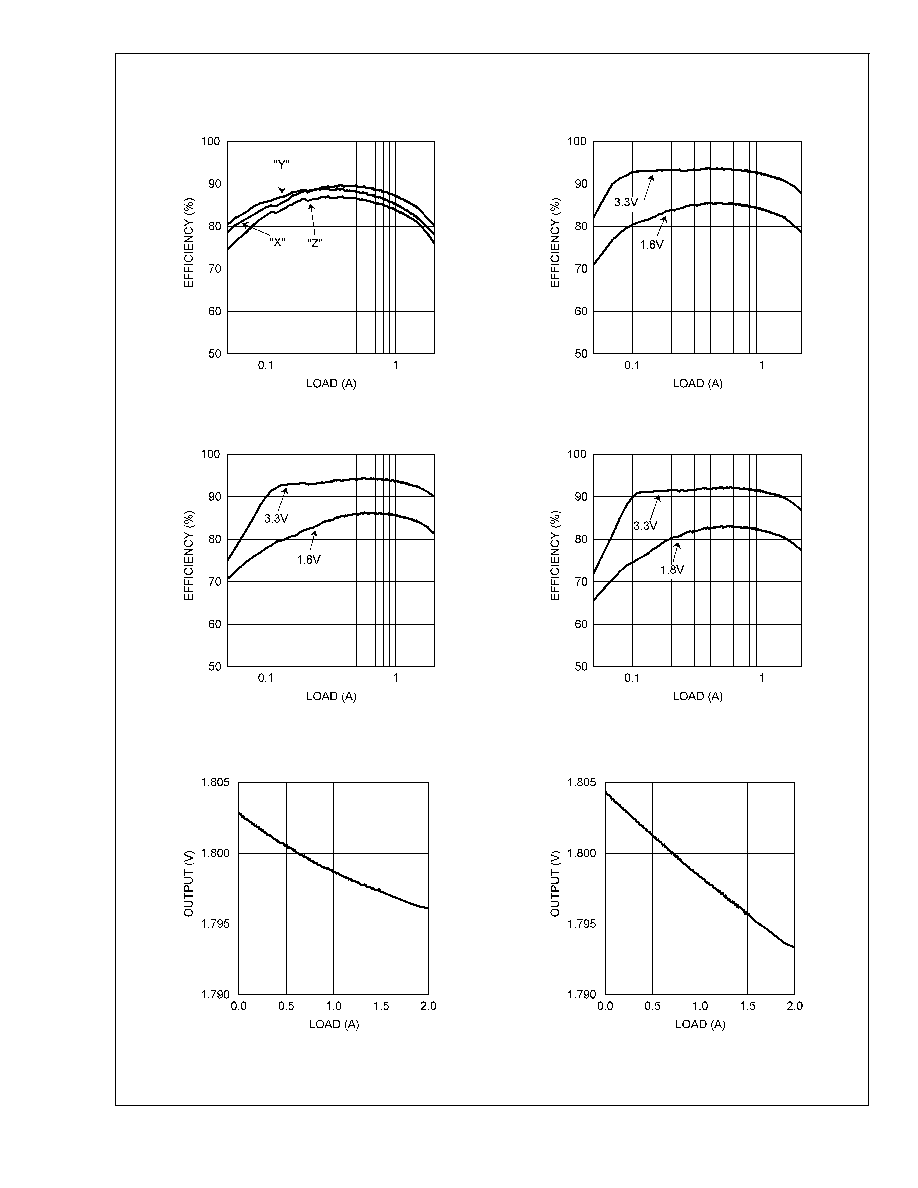
Typical Performance Characteristics
All curves taken at VIN = 5.0V with configuration in typical ap-
plication circuit shown in Application Information section of this datasheet. T
J
= 25∞C, unless otherwise specified.
vs Load "X, Y and Z" Vin = 3.3V, Vo = 1.8V
vs Load "X" Vin = 5V, Vo = 1.8V & 3.3V
20197587
20197539
vs Load - "Y" Vin = 5V, Vo = 3.3V & 1.8V
vs Load "Z" Vin = 5V, Vo = 3.3V & 1.8V
20197590
20197542
Load Regulation
Vin = 3.3V, Vo = 1.8V (All Options)
Load Regulation
Vin = 5V, Vo = 1.8V (All Options)
20197583
20197584
LM2832
www.national.com
6
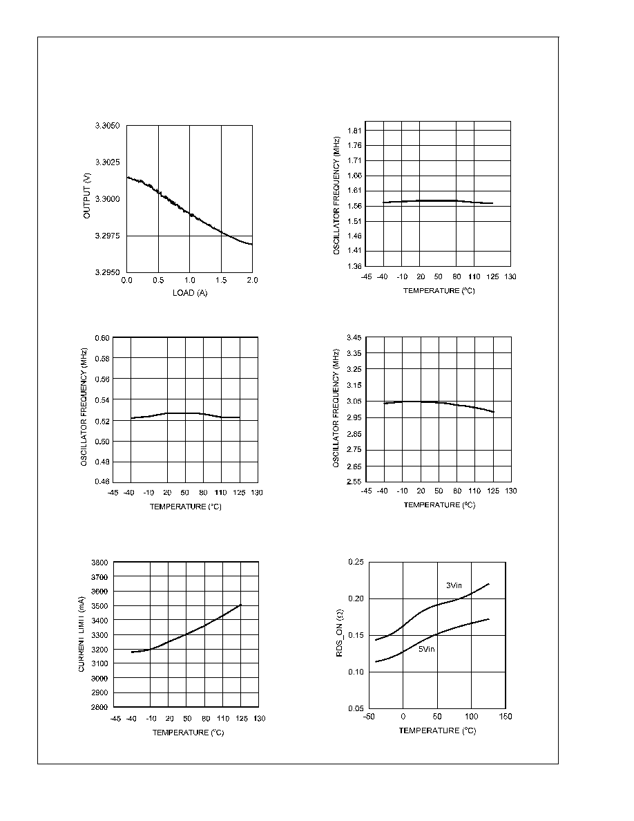
Typical Performance Characteristics
All curves taken at VIN = 5.0V with configuration in typical
application circuit shown in Application Information section of this datasheet. T
J
= 25∞C, unless otherwise
specified. (Continued)
Load Regulation
Vin = 5V, Vo = 3.3V (All Options)
Oscillator Frequency vs Temperature - "X"
20197585
20197524
Oscillator Frequency vs Temperature - "Y"
Oscillator Frequency vs Temperature - "Z"
20197525
20197536
Current Limit vs Temperature
Vin = 3.3V
RDSON vs Temperature (LLP-6 Package)
20197586
20197588
LM2832
www.national.com
7
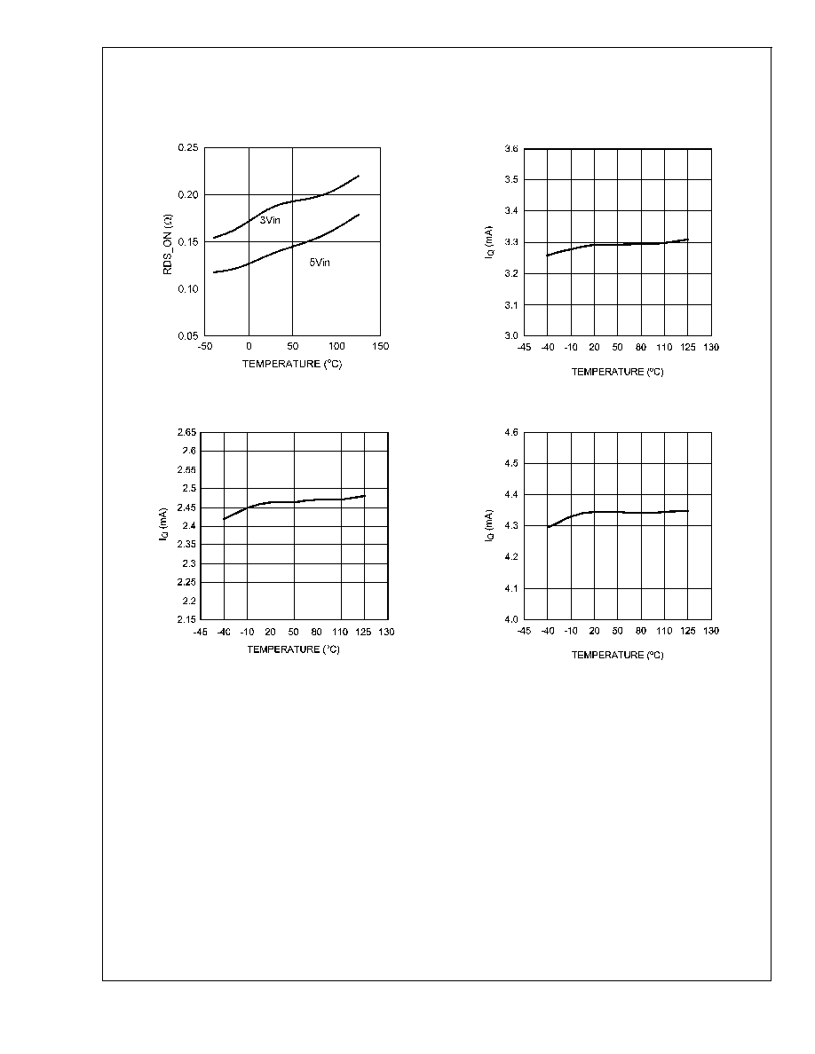
Typical Performance Characteristics
All curves taken at VIN = 5.0V with configuration in typical
application circuit shown in Application Information section of this datasheet. T
J
= 25∞C, unless otherwise
specified. (Continued)
RDSON vs Temperature (eMSOP-8 Package)
LM2832X I
Q
(Quiescent Current)
20197589
20197528
LM2832Y I
Q
(Quiescent Current)
LM2832Z I
Q
(Quiescent Current)
20197529
20197537
LM2832
www.national.com
8

Typical Performance Characteristics
All curves taken at VIN = 5.0V with configuration in typical
application circuit shown in Application Information section of this datasheet. T
J
= 25∞C, unless otherwise
specified. (Continued)
Line Regulation
Vo = 1.8V, Io = 500mA
V
FB
vs Temperature
20197553
20197527
Gain vs Frequency
(Vin = 5V, Vo = 1.2V
@
1A)
Phase Plot vs Frequency
(Vin = 5V, Vo = 1.2V
@
1A)
20197556
20197557
LM2832
www.national.com
9
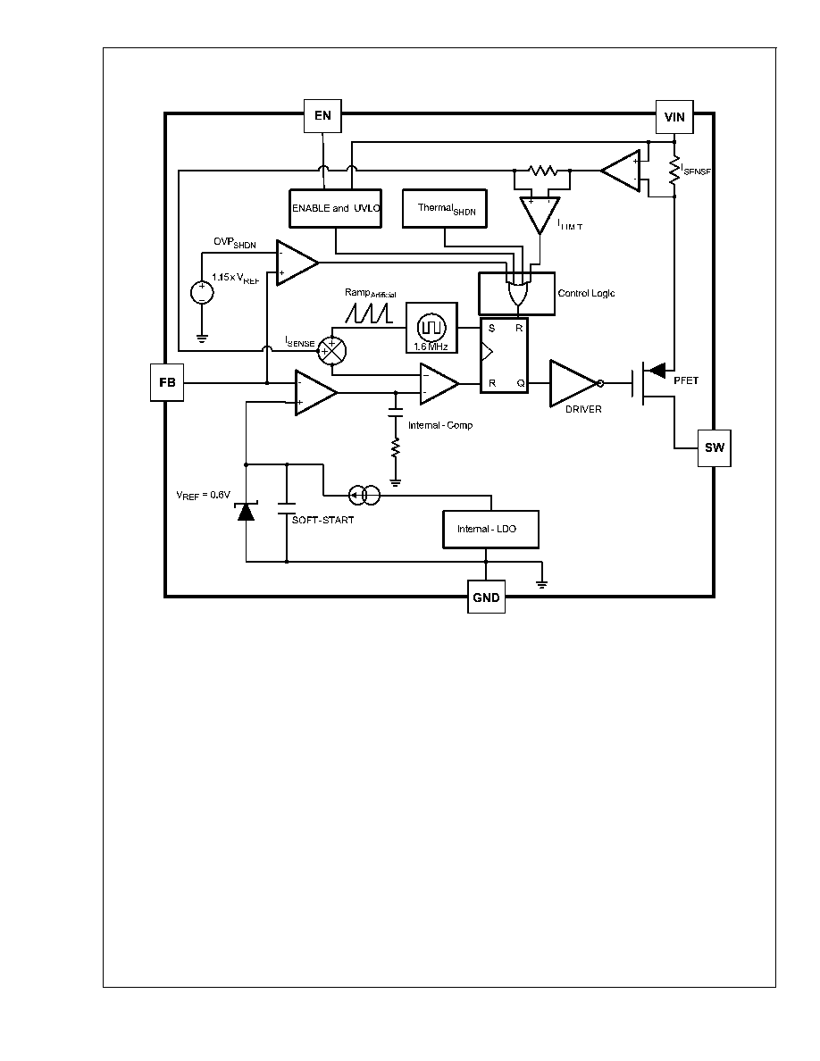
Simplified Block Diagram
20197504
FIGURE 1.
LM2832
www.national.com
10
Applications Information
THEORY OF OPERATION
The LM2832 is a constant frequency PWM buck regulator IC
that delivers a 2.0A load current. The regulator has a preset
switching frequency of 1.6MHz or 3.0MHz. This high fre-
quency allows the LM2832 to operate with small surface
mount capacitors and inductors, resulting in a DC/DC con-
verter that requires a minimum amount of board space. The
LM2832 is internally compensated, so it is simple to use and
requires few external components. The LM2832 uses
current-mode control to regulate the output voltage. The
following operating description of the LM2832 will refer to the
Simplified Block Diagram (Figure 1) and to the waveforms in
Figure 2. The LM2832 supplies a regulated output voltage by
switching the internal PMOS control switch at constant fre-
quency and variable duty cycle. A switching cycle begins at
the falling edge of the reset pulse generated by the internal
oscillator. When this pulse goes low, the output control logic
turns on the internal PMOS control switch. During this on-
time, the SW pin voltage (V
SW
) swings up to approximately
V
IN
, and the inductor current (I
L
) increases with a linear
slope. I
L
is measured by the current sense amplifier, which
generates an output proportional to the switch current. The
sense signal is summed with the regulator's corrective ramp
and compared to the error amplifier's output, which is pro-
portional to the difference between the feedback voltage and
V
REF
. When the PWM comparator output goes high, the
output switch turns off until the next switching cycle begins.
During the switch off-time, inductor current discharges
through the Schottky catch diode, which forces the SW pin to
swing below ground by the forward voltage (V
D
) of the
Schottky catch diode. The regulator loop adjusts the duty
cycle (D) to maintain a constant output voltage.
SOFT-START
This function forces V
OUT
to increase at a controlled rate
during start up. During soft-start, the error amplifier's refer-
ence voltage ramps from 0V to its nominal value of 0.6V in
approximately 600 µs. This forces the regulator output to
ramp up in a controlled fashion, which helps reduce inrush
current.
OUTPUT OVERVOLTAGE PROTECTION
The over-voltage comparator compares the FB pin voltage
to a voltage that is 15% higher than the internal reference
V
REF
. Once the FB pin voltage goes 15% above the internal
reference, the internal PMOS control switch is turned off,
which allows the output voltage to decrease toward regula-
tion.
UNDERVOLTAGE LOCKOUT
Under-voltage lockout (UVLO) prevents the LM2832 from
operating until the input voltage exceeds 2.73V (typ). The
UVLO threshold has approximately 430 mV of hysteresis, so
the part will operate until V
IN
drops below 2.3V (typ). Hys-
teresis prevents the part from turning off during power up if
V
IN
is non-monotonic.
CURRENT LIMIT
The LM2832 uses cycle-by-cycle current limiting to protect
the output switch. During each switching cycle, a current limit
comparator detects if the output switch current exceeds
3.25A (typ), and turns off the switch until the next switching
cycle begins.
THERMAL SHUTDOWN
Thermal shutdown limits total power dissipation by turning
off the output switch when the IC junction temperature ex-
ceeds 165∞C. After thermal shutdown occurs, the output
switch doesn't turn on until the junction temperature drops to
approximately 150∞C.
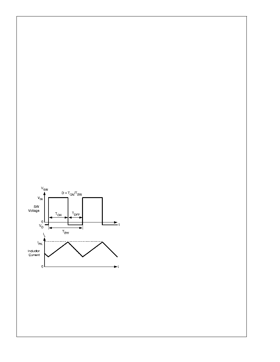
20197566
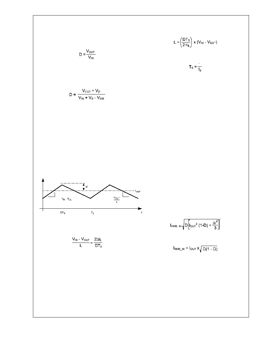
FIGURE 2. Typical Waveforms
LM2832
www.national.com
11
Design Guide
INDUCTOR SELECTION
The Duty Cycle (D) can be approximated quickly using the
ratio of output voltage (V
O
) to input voltage (V
IN
):
The catch diode (D1) forward voltage drop and the voltage
drop across the internal PMOS must be included to calculate
a more accurate duty cycle. Calculate D by using the follow-
ing formula:
V
SW
can be approximated by:
V
SW
= I
OUT
x R
DSON
The diode forward drop (V
D
) can range from 0.3V to 0.7V
depending on the quality of the diode. The lower the V
D
, the
higher the operating efficiency of the converter. The inductor
value determines the output ripple current. Lower inductor
values decrease the size of the inductor, but increase the
output ripple current. An increase in the inductor value will
decrease the output ripple current.
One must ensure that the minimum current limit (2.4A) is not
exceeded, so the peak current in the inductor must be
calculated. The peak current (I
LPK
) in the inductor is calcu-
lated by:
I
LPK
= I
OUT
+
i
L
In general,
i
L
= 0.1 x (I
OUT
)
0.2 x (I
OUT
)
If
i
L
= 20% of 2A, the peak current in the inductor will be
2.4A. The minimum guaranteed current limit over all operat-
ing conditions is 2.4A. One can either reduce
i
L
, or make
the engineering judgment that zero margin will be safe
enough. The typical current limit is 3.25A.
The LM2832 operates at frequencies allowing the use of
ceramic output capacitors without compromising transient
response. Ceramic capacitors allow higher inductor ripple
without significantly increasing output ripple. See the output
capacitor section for more details on calculating output volt-
age ripple. Now that the ripple current is determined, the
inductance is calculated by:
Where
When selecting an inductor, make sure that it is capable of
supporting the peak output current without saturating. Induc-
tor saturation will result in a sudden reduction in inductance
and prevent the regulator from operating correctly. Because
of the speed of the internal current limit, the peak current of
the inductor need only be specified for the required maxi-
mum output current. For example, if the designed maximum
output current is 1.0A and the peak current is 1.25A, then the
inductor should be specified with a saturation current limit of
>
1.25A. There is no need to specify the saturation or peak
current of the inductor at the 3.25A typical switch current
limit. The difference in inductor size is a factor of 5. Because
of the operating frequency of the LM2832, ferrite based
inductors are preferred to minimize core losses. This pre-
sents little restriction since the variety of ferrite-based induc-
tors is huge. Lastly, inductors with lower series resistance
(R
DCR
) will provide better operating efficiency. For recom-
mended inductors see Example Circuits.
INPUT CAPACITOR
An input capacitor is necessary to ensure that V
IN
does not
drop excessively during switching transients. The primary
specifications of the input capacitor are capacitance, volt-
age, RMS current rating, and ESL (Equivalent Series Induc-
tance). The recommended input capacitance is 22 µF.The
input voltage rating is specifically stated by the capacitor
manufacturer. Make sure to check any recommended derat-
ings and also verify if there is any significant change in
capacitance at the operating input voltage and the operating
temperature. The input capacitor maximum RMS input cur-
rent rating (I
RMS-IN
) must be greater than:
Neglecting inductor ripple simplifies the above equation to:
It can be shown from the above equation that maximum
RMS capacitor current occurs when D = 0.5. Always calcu-
late the RMS at the point where the duty cycle D is closest to
0.5. The ESL of an input capacitor is usually determined by
the effective cross sectional area of the current path. A large
leaded capacitor will have high ESL and a 0805 ceramic chip
capacitor will have very low ESL. At the operating frequen-
cies of the LM2832, leaded capacitors may have an ESL so
large that the resulting impedance (2
fL) will be higher than
that required to provide stable operation. As a result, surface
mount capacitors are strongly recommended.
20197505
FIGURE 3. Inductor Current
LM2832
www.national.com
12

Design Guide
(Continued)
Sanyo POSCAP, Tantalum or Niobium, Panasonic SP, and
multilayer ceramic capacitors (MLCC) are all good choices
for both input and output capacitors and have very low ESL.
For MLCCs it is recommended to use X7R or X5R type
capacitors due to their tolerance and temperature character-
istics. Consult capacitor manufacturer datasheets to see
how rated capacitance varies over operating conditions.
OUTPUT CAPACITOR
The output capacitor is selected based upon the desired
output ripple and transient response. The initial current of a
load transient is provided mainly by the output capacitor. The
output ripple of the converter is:
When using MLCCs, the ESR is typically so low that the
capacitive ripple may dominate. When this occurs, the out-
put ripple will be approximately sinusoidal and 90∞ phase
shifted from the switching action. Given the availability and
quality of MLCCs and the expected output voltage of designs
using the LM2832, there is really no need to review any other
capacitor technologies. Another benefit of ceramic capaci-
tors is their ability to bypass high frequency noise. A certain
amount of switching edge noise will couple through parasitic
capacitances in the inductor to the output. A ceramic capaci-
tor will bypass this noise while a tantalum will not. Since the
output capacitor is one of the two external components that
control the stability of the regulator control loop, most appli-
cations will require a minimum of 22 µF of output capaci-
tance. Capacitance often, but not always, can be increased
significantly with little detriment to the regulator stability. Like
the input capacitor, recommended multilayer ceramic ca-
pacitors are X7R or X5R types.
CATCH DIODE
The catch diode (D1) conducts during the switch off-time. A
Schottky diode is recommended for its fast switching times
and low forward voltage drop. The catch diode should be
chosen so that its current rating is greater than:
I
D1
= I
OUT
x (1-D)
The reverse breakdown rating of the diode must be at least
the maximum input voltage plus appropriate margin. To im-
prove efficiency, choose a Schottky diode with a low forward
voltage drop.
OUTPUT VOLTAGE
The output voltage is set using the following equation where
R2 is connected between the FB pin and GND, and R1 is
connected between V
O
and the FB pin. A good value for R2
is 10k
. When designing a unity gain converter (Vo = 0.6V),
R1 should be between 0
and 100, and R2 should be
equal or greater than 10k
.
V
REF
= 0.60V
PCB LAYOUT CONSIDERATIONS
When planning layout there are a few things to consider
when trying to achieve a clean, regulated output. The most
important consideration is the close coupling of the GND
connections of the input capacitor and the catch diode D1.
These ground ends should be close to one another and be
connected to the GND plane with at least two through-holes.
Place these components as close to the IC as possible. Next
in importance is the location of the GND connection of the
output capacitor, which should be near the GND connections
of CIN and D1. There should be a continuous ground plane
on the bottom layer of a two-layer board except under the
switching node island. The FB pin is a high impedance node
and care should be taken to make the FB trace short to avoid
noise pickup and inaccurate regulation. The feedback resis-
tors should be placed as close as possible to the IC, with the
GND of R1 placed as close as possible to the GND of the IC.
The V
OUT
trace to R2 should be routed away from the
inductor and any other traces that are switching. High AC
currents flow through the V
IN
, SW and V
OUT
traces, so they
should be as short and wide as possible. However, making
the traces wide increases radiated noise, so the designer
must make this trade-off. Radiated noise can be decreased
by choosing a shielded inductor. The remaining components
should also be placed as close as possible to the IC. Please
see Application Note AN-1229 for further considerations and
the LM2832 demo board as an example of a four-layer
layout.
LM2832
www.national.com
13

Calculating Efficiency, and
Junction Temperature
The complete LM2832 DC/DC converter efficiency can be
calculated in the following manner.
Or
Calculations for determining the most significant power
losses are shown below. Other losses totaling less than 2%
are not discussed.
Power loss (P
LOSS
) is the sum of two basic types of losses in
the converter: switching and conduction. Conduction losses
usually dominate at higher output loads, whereas switching
losses remain relatively fixed and dominate at lower output
loads. The first step in determining the losses is to calculate
the duty cycle (D):
V
SW
is the voltage drop across the internal PFET when it is
on, and is equal to:
V
SW
= I
OUT
x R
DSON
V
D
is the forward voltage drop across the Schottky catch
diode. It can be obtained from the diode manufactures Elec-
trical Characteristics section. If the voltage drop across the
inductor (V
DCR
) is accounted for, the equation becomes:
The conduction losses in the free-wheeling Schottky diode
are calculated as follows:
P
DIODE
= V
D
x I
OUT
x (1-D)
Often this is the single most significant power loss in the
circuit. Care should be taken to choose a Schottky diode that
has a low forward voltage drop.
Another significant external power loss is the conduction
loss in the output inductor. The equation can be simplified to:
P
IND
= I
OUT
2
x R
DCR
The LM2832 conduction loss is mainly associated with the
internal PFET:
If the inductor ripple current is fairly small, the conduction
losses can be simplified to:
P
COND
= I
OUT
2
x R
DSON
x D
Switching losses are also associated with the internal PFET.
They occur during the switch on and off transition periods,
where voltages and currents overlap resulting in power loss.
The simplest means to determine this loss is to empirically
measuring the rise and fall times (10% to 90%) of the switch
at the switch node.
Switching Power Loss is calculated as follows:
P
SWR
= 1/2(V
IN
x I
OUT
x F
SW
x T
RISE
)
P
SWF
= 1/2(V
IN
x I
OUT
x F
SW
x T
FALL
)
P
SW
= P
SWR
+ P
SWF
Another loss is the power required for operation of the inter-
nal circuitry:
P
Q
= I
Q
x V
IN
I
Q
is the quiescent operating current, and is typically around
2.5mA for the 0.55MHz frequency option.
Typical Application power losses are:
Power Loss Tabulation
V
IN
5.0V
V
OUT
3.3V
P
OUT
5.78W
I
OUT
1.75A
V
D
0.45V
P
DIODE
262mW
F
SW
550kHz
I
Q
2.5mA
P
Q
12.5mW
T
RISE
4nS
P
SWR
10mW
T
FALL
4nS
P
SWF
10mW
R
DS(ON)
150m
P
COND
306mW
IND
DCR
50m
P
IND
153mW
D
0.667
P
LOSS
753mW
88%
P
INTERNAL
339mW
P
COND
+ P
SW
+ P
DIODE
+ P
IND
+ P
Q
= P
LOSS
P
COND
+ P
SWF
+ P
SWR
+ P
Q
= P
INTERNAL
P
INTERNAL
= 339mW
Thermal Definitions
T
J
= Chip junction temperature
T
A
= Ambient temperature
R
JC
= Thermal resistance from chip junction to device case
R
JA
= Thermal resistance from chip junction to ambient air
Heat in the LM2832 due to internal power dissipation is
removed through conduction and/or convection.
Conduction: Heat transfer occurs through cross sectional
areas of material. Depending on the material, the transfer of
heat can be considered to have poor to good thermal con-
ductivity properties (insulator vs. conductor).
Heat Transfer goes as:
Silicon
package lead frame PCB
Convection: Heat transfer is by means of airflow. This could
be from a fan or natural convection. Natural convection
occurs when air currents rise from the hot device to cooler
air.
Thermal impedance is defined as:
LM2832
www.national.com
14

Thermal Definitions
(Continued)
Thermal impedance from the silicon junction to the ambient
air is defined as:
The PCB size, weight of copper used to route traces and
ground plane, and number of layers within the PCB can
greatly effect R
JA
. The type and number of thermal vias can
also make a large difference in the thermal impedance.
Thermal vias are necessary in most applications. They con-
duct heat from the surface of the PCB to the ground plane.
Four to six thermal vias should be placed under the exposed
pad to the ground plane if the LLP package is used.
Thermal impedance also depends on the thermal properties
of the application operating conditions (Vin, Vo, Io etc), and
the surrounding circuitry.
Silicon Junction Temperature Determination Method 1:
To accurately measure the silicon temperature for a given
application, two methods can be used. The first method
requires the user to know the thermal impedance of the
silicon junction to top case temperature.
Some clarification needs to be made before we go any
further.
R
JC
is the thermal impedance from all six sides of an IC
package to silicon junction.
R
JC
is the thermal impedance from top case to the silicon
junction.
In this data sheet we will use R
JC
so that it allows the user
to measure top case temperature with a small thermocouple
attached to the top case.
R
JC
is approximately 30∞C/Watt for the 6-pin LLP package
with the exposed pad. Knowing the internal dissipation from
the efficiency calculation given previously, and the case
temperature, which can be empirically measured on the
bench we have:
Therefore:
T
j
= (R
JC
x P
LOSS
) + T
C
From the previous example:
T
j
= (R
JC
x P
INTERNAL
) + T
C
T
j
= 30∞C/W x 0.339W + T
C
The second method can give a very accurate silicon junction
temperature.
The first step is to determine R
JA
of the application. The
LM2832 has over-temperature protection circuitry. When the
silicon temperature reaches 165∞C, the device stops switch-
ing. The protection circuitry has a hysteresis of about 15∞C.
Once the silicon temperature has decreased to approxi-
mately 150∞C, the device will start to switch again. Knowing
this, the R
JA
for any application can be characterized during
the early stages of the design one may calculate the R
JA
by
placing the PCB circuit into a thermal chamber. Raise the
ambient temperature in the given working application until
the circuit enters thermal shutdown. If the SW-pin is moni-
tored, it will be obvious when the internal PFET stops switch-
ing, indicating a junction temperature of 165∞C. Knowing the
internal power dissipation from the above methods, the junc-
tion temperature, and the ambient temperature R
JA
can be
determined.
Once this is determined, the maximum ambient temperature
allowed for a desired junction temperature can be found.
An example of calculating R
JA
for an application using the
National Semiconductor LM2832 LLP demonstration board
is shown below.
The four layer PCB is constructed using FR4 with
1
/
2
oz
copper traces. The copper ground plane is on the bottom
layer. The ground plane is accessed by two vias. The board
measures 3.0cm x 3.0cm. It was placed in an oven with no
forced airflow. The ambient temperature was raised to
126∞C, and at that temperature, the device went into thermal
shutdown.
From the previous example:
P
INTERNAL
= 339mW
If the junction temperature was to be kept below 125∞C, then
the ambient temperature could not go above 86∞C.
T
j
- (R
JA
x P
LOSS
) = T
A
125∞C - (115∞C/W x 339mW) = 86∞C
LLP Package
For certain high power applications, the PCB land may be
modified to a "dog bone" shape (see Figure 6). By increasing
the size of ground plane, and adding thermal vias, the R
JA
for the application can be reduced.
20197568
FIGURE 4. Internal LLP Connection
LM2832
www.national.com
15
LLP Package
(Continued)
20197506
FIGURE 5. 6-Lead LLP PCB Dog Bone Layout
LM2832
www.national.com
16

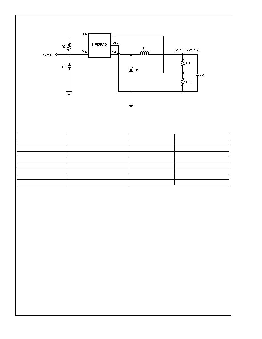
LM2832X Design Example 1
Bill of Materials
Part ID
Part Value
Manufacturer
Part Number
U1
2.0A Buck Regulator
NSC
LM2832X
C1, Input Cap
22µF, 6.3V, X5R
TDK
C3216X5ROJ226M
C2, Output Cap
2x22µF, 6.3V, X5R
TDK
C3216X5ROJ226M
D1, Catch Diode
0.4V
f
Schottky 2A, 20V
R
Diodes Inc.
B220/A
L1
2.2µH, 3.5A
Coilcraft
DS3316P-222
R2
15.0k
, 1%
Vishay
CRCW08051502F
R1
15.0k
, 1%
Vishay
CRCW08051502F
R3
100k
, 1%
Vishay
CRCW08051003F
20197507
FIGURE 6. LM2832X (1.6MHz): Vin = 5V, Vo = 1.2V
@
2.0A
LM2832
www.national.com
17

LM2832X Design Example 2
Bill of Materials
Part ID
Part Value
Manufacturer
Part Number
U1
2.0A Buck Regulator
NSC
LM2832X
C1, Input Cap
22µF, 6.3V, X5R
TDK
C3216X5ROJ226M
C2, Output Cap
2x22µF, 6.3V, X5R
TDK
C3216X5ROJ226M
D1, Catch Diode
0.4V
f
Schottky 2A, 20V
R
Diodes Inc.
B220/A
L1
3.3µH, 3.3A
Coilcraft
DS3316P-332
R2
10.0k
, 1%
Vishay
CRCW08051000F
R1
0
R3
100k
, 1%
Vishay
CRCW08051003F
20197560
FIGURE 7. LM2832X (1.6MHz): Vin = 5V, Vo = 0.6V
@
2.0A
LM2832
www.national.com
18

LM2832X Design Example 3
Bill of Materials
Part ID
Part Value
Manufacturer
Part Number
U1
2.0A Buck Regulator
NSC
LM2832X
C1, Input Cap
22µF, 6.3V, X5R
TDK
C3216X5ROJ226M
C2, Output Cap
2x22µF, 6.3V, X5R
TDK
C3216X5ROJ226M
D1, Catch Diode
0.4V
f
Schottky 2A, 20V
R
Diodes Inc.
B220/A
L1
2.2µH, 2.8A
Coilcraft
ME3220-222
R2
10.0k
, 1%
Vishay
CRCW08051002F
R1
45.3k
, 1%
Vishay
CRCW08054532F
R3
100k
, 1%
Vishay
CRCW08051003F
20197508
FIGURE 8. LM2832X (1.6MHz): Vin = 5V, Vo = 3.3V
@
2.0A
LM2832
www.national.com
19
LM2832Y Design Example 4
Bill of Materials
Part ID
Part Value
Manufacturer
Part Number
U1
1.5A Buck Regulator
NSC
LM2832Y
C1, Input Cap
22µF, 6.3V, X5R
TDK
C3216X5ROJ226M
C2, Output Cap
2x22µF, 6.3V, X5R
TDK
C3216X5ROJ226M
D1, Catch Diode
0.3V
f
Schottky 1.5A, 30V
R
TOSHIBA
CRS08
L1
4.7µH 2.1A
TDK
SLF7045T-4R7M2R0-PF
R1
10.0k
, 1%
Vishay
CRCW08051002F
R2
10.0k
, 1%
Vishay
CRCW08051002F
20197508
FIGURE 9. LM2832Y (550kHz): Vin = 5V, Vout = 3.3V
@
2.0A
LM2832
www.national.com
20

LM2832Y Design Example 5
Bill of Materials
Part ID
Part Value
Manufacturer
Part Number
U1
1.5A Buck Regulator
NSC
LM2832Y
C1, Input Cap
22µF, 6.3V, X5R
TDK
C3216X5ROJ226M
C2, Output Cap
2x22µF, 6.3V, X5R
TDK
C3216X5ROJ226M
D1, Catch Diode
0.3V
f
Schottky 1.5A, 30V
R
TOSHIBA
CRS08
L1
6.8µH 1.8A
TDK
SLF7045T-6R8M1R7
R1
10.0k
, 1%
Vishay
CRCW08051002F
R2
10.0k
, 1%
Vishay
CRCW08051002F
20197507
FIGURE 10. LM2832Y (550kHz): Vin = 5V, Vout = 1.2V
@
2.0A
LM2832
www.national.com
21
LM2832Z Design Example 6
Bill of Materials
Part ID
Part Value
Manufacturer
Part Number
U1
2.0A Buck Regulator
NSC
LM2832Z
C1, Input Cap
22µF, 6.3V, X5R
TDK
C3216X5ROJ226M
C2, Output Cap
2x22µF, 6.3V, X5R
TDK
C3216X5ROJ226M
D1, Catch Diode
0.4V
f
Schottky 2A, 20V
R
Diodes Inc.
B220/A
L1
3.3µH, 3.3A
Coilcraft
DS3316P-332
R2
10.0k
, 1%
Vishay
CRCW08051002F
R1
45.3k
, 1%
Vishay
CRCW08054532F
R3
100k
, 1%
Vishay
CRCW08051003F
20197508
FIGURE 11. LM2832Z (3MHz): Vin = 5V, Vo = 3.3V
@
2.0A
LM2832
www.national.com
22
LM2832Z Design Example 7
Bill of Materials
Part ID
Part Value
Manufacturer
Part Number
U1
2.0A Buck Regulator
NSC
LM2832Z
C1, Input Cap
22µF, 6.3V, X5R
TDK
C3216X5ROJ226M
C2, Output Cap
2x22µF, 6.3V, X5R
TDK
C3216X5ROJ226M
D1, Catch Diode
0.4V
f
Schottky 2A, 20V
R
Diodes Inc.
B220/A
L1
4.7µH, 2.7A
Coilcraft
DS3316P-472
R2
10.0k
, 1%
Vishay
CRCW08051002F
R1
10.0k
, 1%
Vishay
CRCW08051002F
R3
100k
, 1%
Vishay
CRCW08051003F
20197507
FIGURE 12. LM2832Z (3MHz): Vin = 5V, Vo = 1.2V
@
2.0A
LM2832
www.national.com
23

LM2832X Dual Converters with Delayed Enabled Design Example 8
Bill of Materials
Part ID
Part Value
Manufacturer
Part Number
U1, U2
2.0A Buck Regulator
NSC
LM2832X
U3
Power on Reset
NSC
LP3470M5X-3.08
C1, C3 Input Cap
22µF, 6.3V, X5R
TDK
C3216X5ROJ226M
C2, C4 Output Cap
2x22µF, 6.3V, X5R
TDK
C3216X5ROJ226M
C7
Trr delay capacitor
TDK
D1, D2 Catch Diode
0.4V
f
Schottky 2A, 20V
R
Diodes Inc.
B220/A
L1, L2
3.3µH, 2.7A
Coilcraft
ME3220-102
R2, R4, R5
10.0k
, 1%
Vishay
CRCW08051002F
R1, R6
45.3k
, 1%
Vishay
CRCW08054532F
R3
100k
, 1%
Vishay
CRCW08051003F
20197562
FIGURE 13. LM2832X (1.6MHz): Vin = 5V, Vo = 1.2V
@
2.0A & 3.3V
@
2.0A
LM2832
www.national.com
24
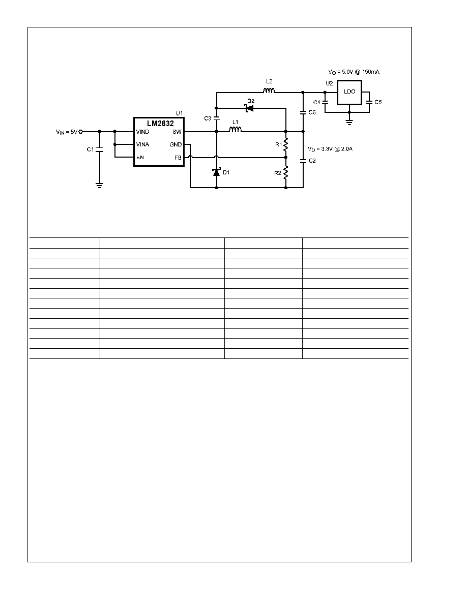
LM2832X Buck Converter & Voltage Double Circuit with LDO Follower
Design Example 9
Bill of Materials
Part ID
Part Value
Manufacturer
Part Number
U1
2.0A Buck Regulator
NSC
LM2832X
U2
200mA LDO
NSC
LP2986-5.0
C1, Input Cap
22µF, 6.3V, X5R
TDK
C3216X5ROJ226M
C2, Output Cap
2x22µF, 6.3V, X5R
TDK
C3216X5ROJ226M
C3 ≠ C6
2.2µF, 6.3V, X5R
TDK
C1608X5R0J225M
D1, Catch Diode
0.4V
f
Schottky 2A, 20V
R
Diodes Inc.
B220/A
D2
0.4V
f
Schottky 20V
R
, 500mA
ON Semi
MBR0520
L2
10µH, 800mA
CoilCraft
ME3220-103
L1
2.2µH, 3.5A
CoilCraft
DS3316P-222
R2
45.3k
, 1%
Vishay
CRCW08054532F
R1
10.0k
, 1%
Vishay
CRCW08051002F
20197563
FIGURE 14. LM2832X (1.6MHz): Vin = 5V, Vo = 3.3V
@
2.0A & LP2986-5.0
@
150mA
LM2832
www.national.com
25
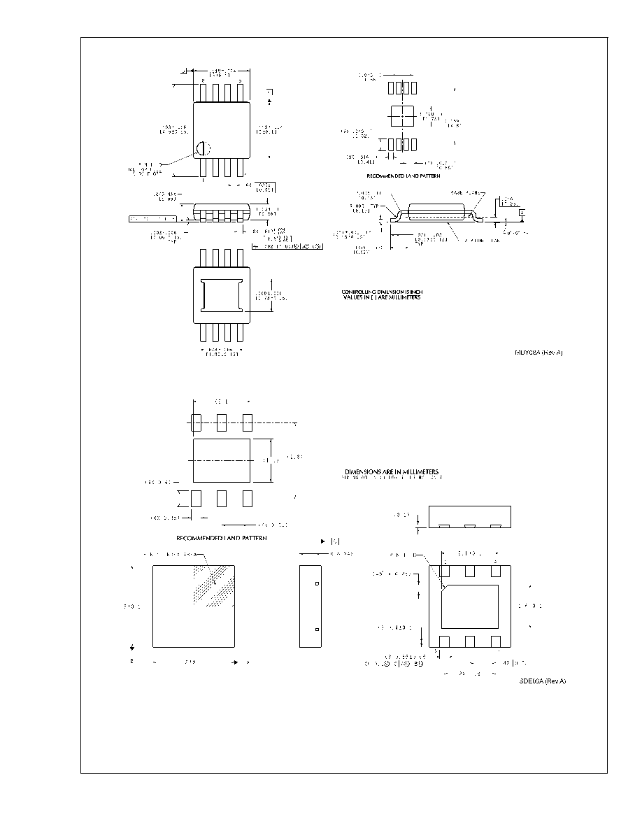
Physical Dimensions
inches (millimeters) unless otherwise noted
8-Lead eMSOP Package
NS Package Number MUY08A
6-Lead LLP Package
NS Package Number SDE06A
LM2832
www.national.com
26
Notes
National does not assume any responsibility for use of any circuitry described, no circuit patent licenses are implied and National reserves
the right at any time without notice to change said circuitry and specifications.
For the most current product information visit us at www.national.com.
LIFE SUPPORT POLICY
NATIONAL'S PRODUCTS ARE NOT AUTHORIZED FOR USE AS CRITICAL COMPONENTS IN LIFE SUPPORT DEVICES OR SYSTEMS
WITHOUT THE EXPRESS WRITTEN APPROVAL OF THE PRESIDENT AND GENERAL COUNSEL OF NATIONAL SEMICONDUCTOR
CORPORATION. As used herein:
1. Life support devices or systems are devices or systems
which, (a) are intended for surgical implant into the body, or
(b) support or sustain life, and whose failure to perform when
properly used in accordance with instructions for use
provided in the labeling, can be reasonably expected to result
in a significant injury to the user.
2. A critical component is any component of a life support
device or system whose failure to perform can be reasonably
expected to cause the failure of the life support device or
system, or to affect its safety or effectiveness.
BANNED SUBSTANCE COMPLIANCE
National Semiconductor follows the provisions of the Product Stewardship Guide for Customers (CSP-9-111C2) and Banned Substances
and Materials of Interest Specification (CSP-9-111S2) for regulatory environmental compliance. Details may be found at:
www.national.com/quality/green.
Lead free products are RoHS compliant.
National Semiconductor
Americas Customer
Support Center
Email: new.feedback@nsc.com
Tel: 1-800-272-9959
National Semiconductor
Europe Customer Support Center
Fax: +49 (0) 180-530 85 86
Email: europe.support@nsc.com
Deutsch Tel: +49 (0) 69 9508 6208
English
Tel: +44 (0) 870 24 0 2171
FranÁais Tel: +33 (0) 1 41 91 8790
National Semiconductor
Asia Pacific Customer
Support Center
Email: ap.support@nsc.com
National Semiconductor
Japan Customer Support Center
Fax: 81-3-5639-7507
Email: jpn.feedback@nsc.com
Tel: 81-3-5639-7560
www.national.com
LM2832
High
Frequency
2.0A
Load
-
Step-Down
DC-DC
Regulator