LM2852
2A 500/1500kHz SIMPLE SYNCHRONOUS
TM
Buck
Regulator
General Description
The LM2852 SIMPLE SYNCHRONOUS
TM
buck regulator is
a high frequency step-down switching voltage regulator ca-
pable of driving up to a 2A load with excellent line and load
regulation. The LM2852 can accept an input voltage be-
tween 2.85V and 5.5V and deliver a customizable output
voltage that is factory programmable from 0.8V to 3.3V in
100mV increments. The LM2852 is available with a choice of
two switching frequencies - 500kHz (LM2852Y) or 1.5MHz
(LM2852X). It also features internal compensation to deliver
a
low
component
count
solution.
The
exposed-pad
TSSOP-14 package enhances the thermal performance of
the LM2852.
Features
n
Input voltage range of 2.85 to 5.5V
n
Factory EEPROM set output voltages from 0.8V to 3.3V
in 100mV increments
n
Maximum Load Current of 2A
n
Voltage Mode Control
n
Internal type three compensation
n
Switching frequency of 500kHz or 1.5MHz
n
Low standby current of 10µA
n
Internal 60 m
MOSFET switches
n
Standard voltage options 1.0/1.2/1.5/1.8/2.5/3.3 volts
Applications
n
Low voltage point of load regulators
n
Local solution for FPGA/DSP/ASIC core power
n
Broadband networking and communications
infrastructure
n
Portable computing
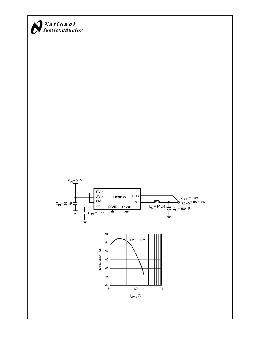
Typical Application Circuit
20127001
20127002
January 2005
LM2852
2A
500/1500kHz
SIMPLE
SYNCHRONOUS
Buck
Regulator
© 2005 National Semiconductor Corporation
DS201270
www.national.com
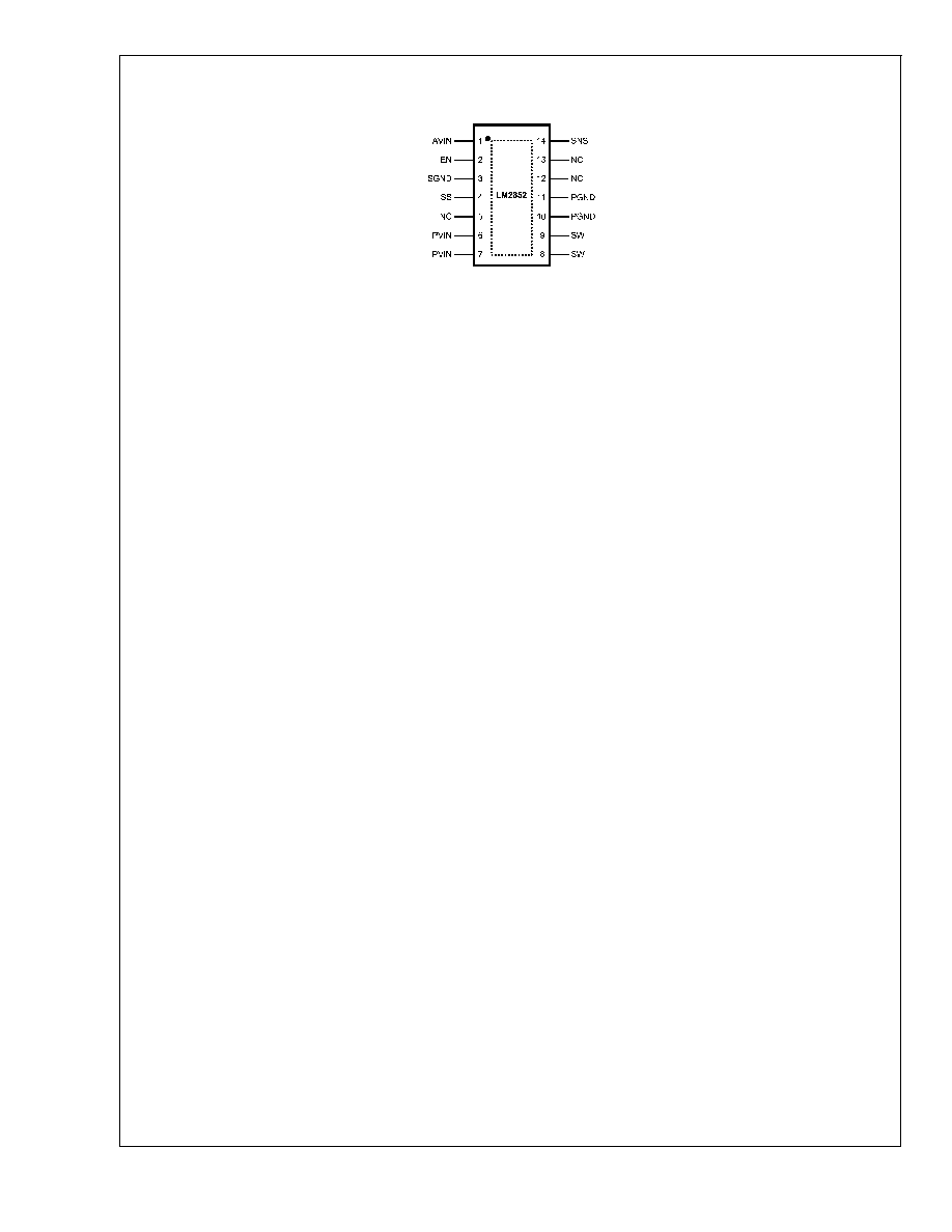
Connection Diagram
TOP VIEW
20127003
MXA14A
Pin Descriptions
AVIN (Pin 1): Chip bias input pin. This provides power to the
logic of the chip. Connect to the input voltage or a separate
rail.
EN (Pin 2): Enable. Connect this pin to ground to disable the
chip, connect to AVIN or leave floating to enable the chip;
enable is internally pulled up.
SGND (Pin 3): Low-noise ground.
SS (Pin 4): Soft-start pin. Connect this pin to a small capaci-
tor to control startup and soften inrush current. The soft-start
capacitance range is restricted to values 1 nF to 50 nF.
NC (Pins 5, 12 and 13): No-connect. These pins must be
tied to ground or left floating in the application.
PVIN (Pins 6, 7): Input supply pin. PVIN is connected to the
input voltage. This rail connects to the source of the internal
power PFET.
SW (Pins 8, 9): Switch pin. Connect to the output inductor.
PGND (Pins 10, 11): Power ground. Connect this to an
internal ground plane or other large ground plane.
SNS (Pin 14): Output voltage sense pin. Connect this pin to
the output voltage as close to the load as possible.
Exposed Pad: Connect to ground.
LM2852
www.national.com
2

Ordering Information
Order Number
Frequency
Voltage Option
Package Type
Package Drawing
Supplied As
LM2852YMXA-1.0
500kHz
1.0
TSSOP-14 exposed pad
MXA14A
94 Units, Rail
LM2852YMXAX-1.0
2500 Units, Tape and
Reel
LM2852YMXA-1.2
1.2
94 Units, Rail
LM2852YMXAX-1.2
2500 Units, Tape and
Reel
LM2852YMXA-1.5
1.5
94 Units, Rail
LM2852YMXAX-1.5
2500 Units, Tape and
Reel
LM2852YMXA-1.8
1.8
94 Units, Rail
LM2852YMXAX-1.8
2500 Units, Tape and
Reel
LM2852YMXA-2.5
2.5
94 Units, Rail
LM2852YMXAX-2.5
2500 Units, Tape and
Reel
LM2852YMXA-3.3
3.3
94 Units, Rail
LM2852YMXAX-3.3
2500 Units, Tape and
Reel
LM2852XMXA-1.0
1500kHz
1.0
Coming Soon
LM2852XMXAX-1.0
LM2852XMXA-1.2
1.2
LM2852XMXAX-1.2
LM2852XMXA-1.5
1.5
LM2852XMXAX-1.5
LM2852XMXA-1.8
1.8
LM2852XMXAX-1.8
LM2852XMXA-2.5
2.5
LM2852XMXAX-2.5
LM2852XMXA-3.3
3.3
LM2852XMXAX-3.3
Note: Contact factory for other voltage options.
LM2852
www.national.com
3
Absolute Maximum Ratings
(Note 1)
If Military/Aerospace specified devices are required,
please contact the National Semiconductor Sales Office/
Distributors for availability and specifications.
PVIN, AVIN, EN, SNS
-0.3V to 6.5V
ESD Susceptibility (Note 2)
2kV
Power Dissipation
Internally Limited
Storage Temperature Range
-65∞C to +150∞C
Maximum Junction Temp.
150∞C
14-Pin Exposed Pad TSSOP
Package
Infrared (15 sec)
Vapor Phase (60 sec)
Soldering (10 sec)
220∞C
215∞C
260∞C
Operating Ratings
PVIN to GND
1.5V to 5.5V
AVIN to GND
2.85V to 5.5V
Junction Temperature
-40∞C to +125∞C
JA
37.6∞C/W
Electrical Characteristics
AVIN = PVIN = 5V unless otherwise indicated under the Conditions column.
Typicals and limits appearing in plain type apply for T
A
= T
J
= +25∞C. Limits appearing in boldface type apply over full Oper-
ating Junction Temperature Range (-40∞C to +125∞C). Datasheet min/max specification limits are guaranteed by design, test,
or statistical analysis.
Symbol
Parameter
Conditions
Min
Typ
Max
Units
SYSTEM PARAMETERS
V
OUT
Voltage Tolerance
3
V
OUT
= 1.0V option
0.9775
1.0225
V
V
OUT
= 1.2V option
1.1730
1.2270
V
OUT
= 1.5V option
1.4663
1.5337
V
OUT
= 1.8V option
1.7595
1.8405
V
OUT
= 2.5V option
2.4437
2.5563
V
OUT
= 3.3V option
3.2257
3.3743
V
OUT
/
AVIN
Line Regulation
3
V
OUT
= 0.8V, 1.0V, 1.2V, 1.5V, 1.8V or
2.5V
2.85V
AVIN 5.5V
0.2
0.6
%
V
OUT
= 3.3V
3.5V
AVIN 5.5V
0.2
0.6
%
V
OUT
/
I
O
Load Regulation
Normal operation
8
mV/A
V
ON
UVLO Threshold
(AVIN)
Rising
2.47
2.85
V
Falling Hysteresis
85
150
210
mV
r
DSON-P
PFET On
Resistance
Isw = 2A
75
140
m
r
DSON-N
NFET On
Resistance
Isw = 2A
55
120
m
R
SS
Soft-start
resistance
400
k
I
CL
Peak Current Limit
Threshold
2.25
3
3.65
A
I
Q
Operating Current Non-switching
0.85
2
mA
I
SD
Shut Down
Quiescent Current
EN = 0V
10
25
µA
R
SNS
Sense pin
resistance
400
k
PWM
f
osc
LM2852X
1500kHz option.
TBD
1500
TBD
kHz
LM2852Y
500kHz option.
325
500
625
kHz
D
range
Duty Cycle Range
0
100
%
LM2852
www.national.com
4
Electrical Characteristics
AVIN = PVIN = 5V unless otherwise indicated under the Conditions column.
Typicals and limits appearing in plain type apply for T
A
= T
J
= +25∞C. Limits appearing in boldface type apply over full
Operating Junction Temperature Range (-40∞C to +125∞C). Datasheet min/max specification limits are guaranteed by design,
test, or statistical analysis. (Continued)
Symbol
Parameter
Conditions
Min
Typ
Max
Units
ENABLE CONTROL
4
V
IH
EN Pin Minimum
High Input
75
% of
AVIN
V
IL
EN Pin Maximum
Low Input
25
% of
AVIN
I
EN
EN Pin Pullup
Current
EN = 0V
1.2
µA
THERMAL CONTROLS
T
SD
T
J
for Thermal
Shutdown
165
∞C
T
SD-hys
Hysteresis for
Thermal Shutdown
10
∞C
Note 1: Absolute maximum ratings indicate limits beyond which damage to the device may occur. Operating Range indicates conditions for which the device is
intended to be functional, but does not guarantee specfic performance limits. For guaranteed specifications and test conditions, see the Electrical Characteristics.
Note 2: Human body model: 1.5k
in series with 100pF. SW and PVIN pins are derated to 1.5kV
Note 3: V
OUT
measured in a non-switching, closed-loop configuration at the SNS pin.
Note 4: The enable pin is internally pulled up, so the LM2852 is automatically enabled unless an external enable voltage is applied.
LM2852
www.national.com
5