 | –≠–ª–µ–∫—Ç—Ä–æ–Ω–Ω—ã–π –∫–æ–º–ø–æ–Ω–µ–Ω—Ç: LM2889N | –°–∫–∞—á–∞—Ç—å:  PDF PDF  ZIP ZIP |
TL H 5079
LM2889
TV
Video
Modulator
December 1994
LM2889 TV Video Modulator
General Description
The LM2889 is designed to interface audio and video sig-
nals to the antenna terminals of a TV receiver It consists of
a sound subcarrier oscillator and FM modulator video
clamp and RF oscillators and modulators for two low-VHF
channels
The LM2889 allows video information from VTRs video disk
systems games test equipment or similar sources to be
displayed on black and white or color TV receivers
Features
Y
Pin for pin compatible with LM1889 RF section
Y
Low distortion FM sound modulator (less than 1%
THD)
Y
Video clamp for AC-coupled video
Y
Low sound oscillator harmonic levels
Y
10V to 16V supply operation
Y
DC channel switching
Y
Excellent oscillator stability
Y
Low intermodulation products
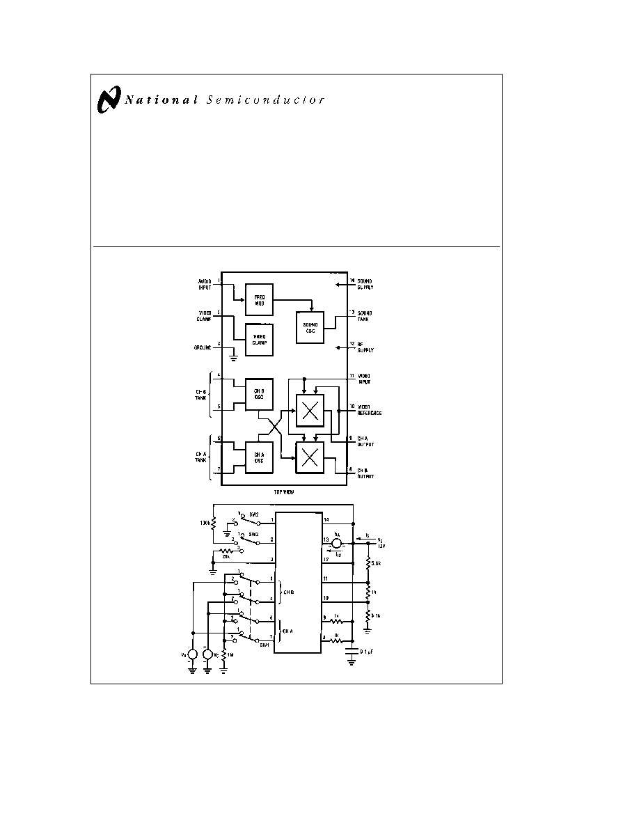
Block and Connection Diagrams
(Dual-In-Line Package)
DC Test Circuit
TL H 5079 ≠ 1
Order Number LM2889N
See NS Package Number N14A
C1995 National Semiconductor Corporation
RRD-B30M115 Printed in U S A

Absolute Maximum Ratings
If Military Aerospace specified devices are required
please contact the National Semiconductor Sales
Office Distributors for availability and specifications
Supply Voltage
18V
DC
Power Dissipation Package (Note 1)
700 mW
Operating Temperature Range
0 C to
a
70 C
Storage Temperature Range
b
55 C to
a
150 C
(V14 ≠ V13) Max
g
5V
DC
(V12 ≠ V8) Max
7V
DC
(V12 ≠ V9) Max
7V
DC
Lead Temperature (Soldering 10 seconds)
260 C
DC Electrical Characteristics
(DC test circuit all switches normally pos 1 V
S
e
12V V
A
e
2V V
B
e
V
C
e
10V)
Parameter
Conditions
Min
Typ
Max
Units
Supply Current I
S
10
16
25
mA
Sound Oscillator Current DI
13
Change V
A
from
b
2V to
a
2V
0 2
0 35
0 6
mA
Sound Oscillator Zener Current I
13
0 85
mA
Sound Modulator Audio Current DI
13
Change SW2 from Pos 1 to Pos 2
0 9
mA
Video Clamp Voltage V2
Unloaded
5 0
5 25
5 5
V
DC
Loaded
SW3 Pos 3
5 1
V
DC
Video Clamp Capacitor Discharge
SW3 Pos 2
20
m
A
Current (V
S
≠ V2) 10
5
Ch A Oscillator OFF Voltage V6 V7
SW1 Pos 2
2
mV
DC
Ch A Oscillator Current Level I
7
V
B
e
10V V
C
e
11V
2 5
3 5
5 0
mA
Ch B Oscillator OFF Voltage V4 V5
2
mV
DC
Ch B Oscillator Current Level I
4
SW1 Pos 2 V
B
e
10V V
C
e
11V
2 5
3 5
5 0
mA
Ch A Modulator Conversion Ratio
Measure DV9 by Changing from
D
V9 (V11-V10)
V
B
e
10V V
C
e
11V to V
B
e
11V
0 3
0 50
0 75
V V
V
C
e
10V Divide by V11 ≠ V10
Ch B Modulator Conversion Ratio
SW1 Pos 2 Measure DV8 by
D
V8 (V11 ≠ V10)
Changing from V
B
e
10V V
C
e
11V
0 3
0 50
0 75
V V
to V
B
e
11V V
C
e
10V Divide by
V11 ≠ V10
AC Electrical Characteristics
(AC test circuit V
S
e
12V)
Parameter
Conditions
Min
Typ
Max
Units
Sound Carrier Oscillator Level V
Vp p
Sound Modulator Deviation
D
f DV
IN
SW Pos
Change V
IN
from
V
Hz mV
to
V Measure Df at Pin
Divide as Shown
Ch
RF Oscillator Level n
n
Ch Sw Pos
f
e
MHz Use FET Probe
mVp p
Ch
RF Oscillator Level n
n
Ch Sw Pos
f
e
MHz Use FET Probe
mVp p
RF Modulator Conversion Gain n
OUT
V
V
Ch Sw Pos
f
e
MHz Note
mVrms V
Note 1
For operation in ambient temperatures above 25 C the device must be derated based on a 150 C maximum junction temperature and a thermal resistance
of 80 C W junction to ambient
Note 2
Conversion gain shown is measured with 75X input RF meter which makes the AC RF output load 37 5X
2

Design Characteristics
(AC test circuit V
S
e
12V)
Parameter
Typ
Units
Sound Modulator Audio THD at
g
25 kHz Deviation V
IN
must be 1 kHz Source
0 8
%
Demodulate as Shown in
Figure 1
Sound Modulator Input Impedance (Pin 1)
1 5
kX
Sound Modulator Bandwidth
100
kHz
Oscillator Supply Dependence Sound Carrier RF
See Curves
Oscillator Temperature Dependence (IC Only)
Sound Carrier
b
15
ppm C
RF
b
50
ppm C
RF Oscillator Maximum Operating Frequency (Temperature Stability Degraded)
100
MHz
RF Modulator
Carrier Suppression (Adjust Video Bias for Minimum RF Carrier at n
OUT
30
dB
and Reference to n
OUT
with 3V Offset at Pins 10 and 11 See Applications
Information RF Modulation Section)
3 58 MHz Differential Gain
5
%
Differential Phase
3
degrees
2 5V Vp-p Video 87 5% Mod
Output Harmonics below RF Carrier
2nd 3rd
b
12
dB
4th and Above
b
20
dB
Input Impedance Pin 10 Pin 11
1 MX
2 pF
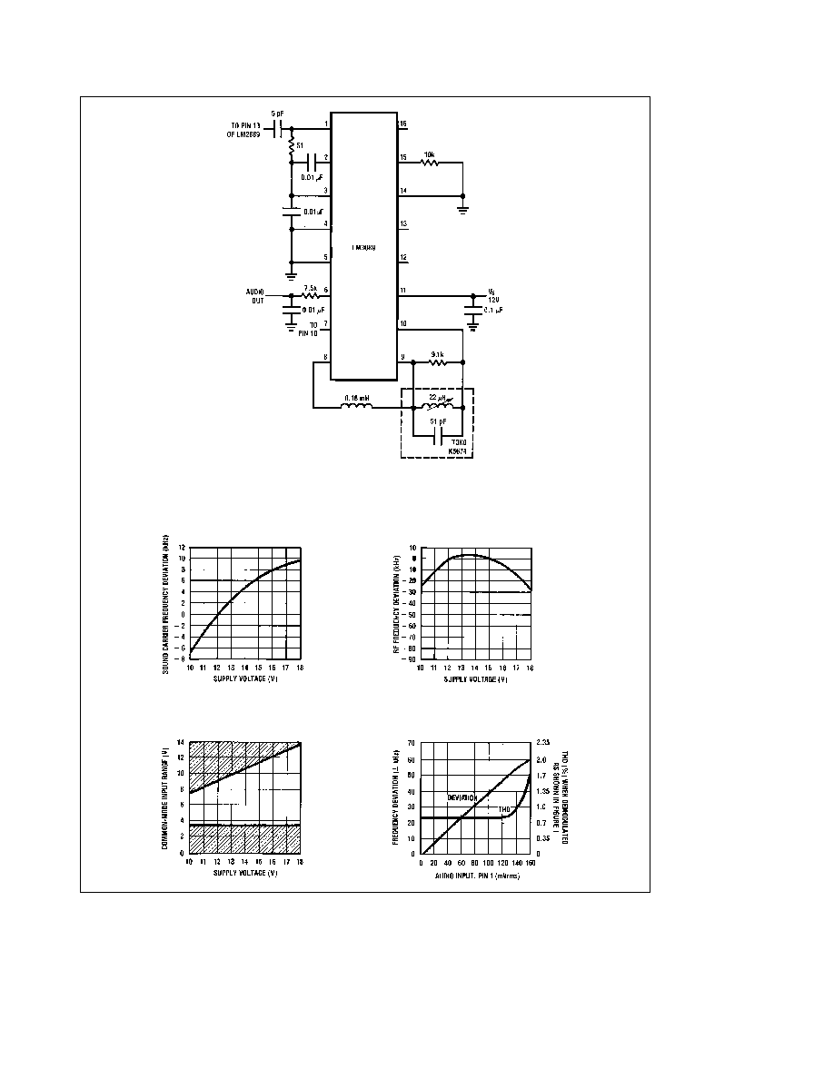
AC Test Circuit
TL H 5079 ≠ 2
3
Test Circuit
TL H 5079 ≠ 3
FIGURE 1 4 5 MHz Sound FM Demodulator
Typical Performance Characteristics
(Refer to AC test circuit unless noted)
Sound Carrier Oscillator
Supply Dependence
(f
O
e
4 5 MHz Pin 1 Open)
RF Oscillator Frequency
Supply Dependence
(f
O
e
67 25 MHz)
RF Modulator Common-
Mode Input Range
Pins 10 11 (Circuit
Diagrams)
FM Sound Modulator
Dynamic Characteristics
(f
MOD
e
1 kHz)
TL H 5079 ≠ 4
4
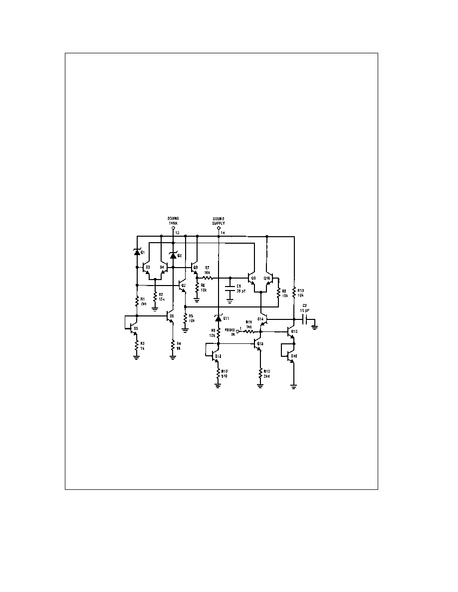
Circuit Description
(Refer to Circuit Diagrams)
The sound carrier oscillator is formed by differential amplifi-
er Q3 Q4 operated with positive feedback from the pin 13
tank to the base of Q4 Frequency modulation is obtained
by varying the 90 degree phase shifted current of Q9 Q14's
emitter is a virtual ground so the voltage at pin 1 deter-
mines the current R11 which ultimately modulates the col-
lector current of Q9
The video clamp is comprised of devices Q58-Q60 The
clamp voltage is set by resistors R40 R41 R49 and R50
The DV
BE
R42 current sets the capacitor discharge cur-
rent Q59 and the above mentioned resistor string help
maintain a temperature stable clamp voltage
The channel B oscillator consists of devices Q24 and Q25
cross-coupled through level-shift zener diodes Q22 and
Q23 A current regulator consisting of devices Q17 ≠ Q21 is
used to achieve good RF stability over temperature and
supply The channel B modulator consists of multiplier de-
vices Q28 ≠ Q31 Q34 and Q35 The top quad is coupled to
the channel B tank through isolating devices Q26 and Q27
A DC potential between pins 10 and 11 offsets the lower
pair to produce an output RF carrier at pin 8 That carrier is
then modulated by both the sound subcarrier at pin 10 and
the composite video signal at pin 11 The channel A modu-
lator shares pin 10 and 11 buffers Q32 and Q33 with chan-
nel B and operates in an identical manner
The current flowing through channel B oscillator diodes
Q22 Q23 is turned around in Q36 ≠ Q38 to source current
for the channel B RF modulator In the same manner the
channel A oscillator Q54 ≠ Q57 uses turn-around Q49 ≠ Q51
to source the channel A modulator One oscillator at a time
may be activated by its current turn-around and the other
oscillator modulator combination remains off
Circuit Diagrams
TL H 5079 ≠ 5
5