LM2984
Microprocessor Power Supply System
General Description
The LM2984 positive voltage regulator features three inde-
pendent and tracking outputs capable of delivering the
power for logic circuits, peripheral sensors and standby
memory in a typical microprocessor system. The LM2984 in-
cludes circuitry which monitors both its own high-current out-
put and also an external µP. If any error conditions are
sensed in either, a reset error flag is set and maintained until
the malfunction terminates. Since these functions are in-
cluded in the same package with the three regulators, a
great saving in board space can be realized in the typical mi-
croprocessor system. The LM2984 also features very low
dropout voltages on each of its three regulator outputs (0.6V
at the rated output current). Furthermore, the quiescent cur-
rent can be reduced to 1 mA in the standby mode.
Designed also for vehicular applications, the LM2984 and all
regulated circuitry are protected from reverse battery instal-
lations or 2-battery jumps. Familiar regulator features such
as short circuit and thermal overload protection are also pro-
vided. Fixed outputs of 5V are available in the plastic TO-220
power package.
Features
n
Three low dropout tracking regulators
n
Output current in excess of 500 mA
n
Fully specified for -40∞C to +125∞C operation
n
Low quiescent current standby regulator
n
Microprocessor malfunction RESET flag
n
Delayed RESET on power-up
n
Accurate pretrimmed 5V outputs
n
Reverse battery protection
n
Overvoltage protection
n
Reverse transient protection
n
Short circuit protection
n
Internal thermal overload protection
n
ON/OFF switch for high current outputs
n
P
+
Product Enhancement tested
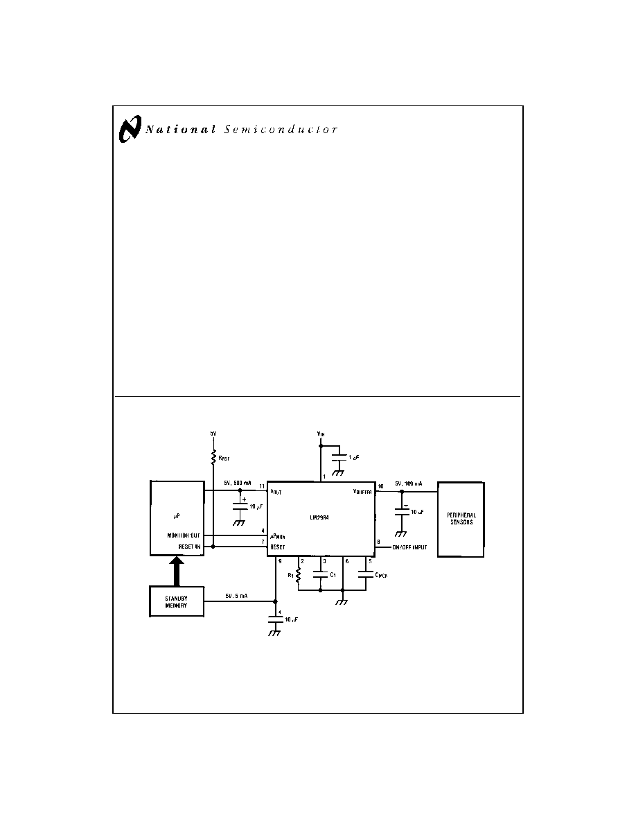
Typical Application Circuit
DS011252-1
C
OUT
must be at least 10 µF to maintain stability. May be increased without bound to maintain regulation during transients. Locate as close as possible to
the regulator. This capacitor must be rated over the same operating temperature range as the regulator. The equivalent series resistance (ESR) of this
capacitor is critical; see curve.
Order Number LM2984T
See NS Package Number TA11B
April 1998
LM2984
Microprocessor
Power
Supply
System
© 1998 National Semiconductor Corporation
DS011252
www.national.com
Absolute Maximum Ratings
(Note 2)
If Military/Aerospace specified devices are required,
please contact the National Semiconductor Sales Office/
Distributors for availability and specifications.
Input Voltage
Survival Voltage (
<
100 ms)
60V
Operational Voltage
26V
Internal Power Dissipation
Internally Limited
Operating Temperature Range (T
A
)
-40∞C to +125∞C
Maximum Junction Temperature
(Note 3)
150∞C
Storage Temperature Range
-65∞C to +150∞C
Lead Temperature
(Soldering, 10 sec.)
230∞C
ESD Susceptability (Note 5)
2000V
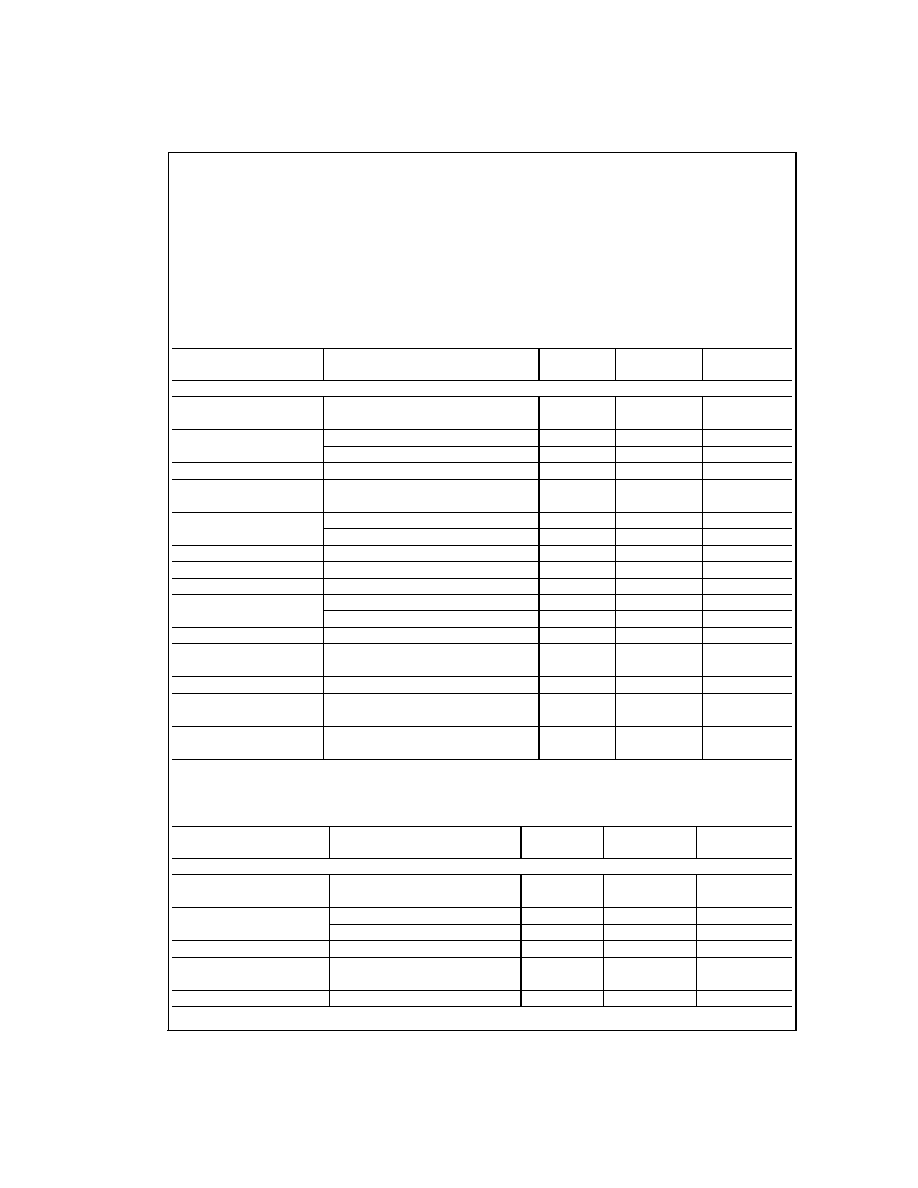
Electrical Characteristics
V
IN
= 14V, I
OUT
= 5 mA, C
OUT
= 10 µF, unless otherwise indicated. Boldface type refers to limits over the entire operating
temperature range, -40∞C
T
A
+125∞C, all other limits are for T
A
= T
j
= 25∞C (Note 8) .
Parameter
Conditions
Typical
Limit
Units
(Note 4)
V
OUT
(Pin 11)
Output Voltage
5 mA
I
O
500 mA
5.00
4.85/4.75
V
min
6V
V
IN
26V
5.15/5.25
V
max
Line Regulation
9V
V
IN
16V
2
25/25
mV
max
7V
V
IN
26V
5
50/50
mV
max
Load Regulation
5 mA
I
OUT
500 mA
12
50/50
mV
max
Output Impedance
250 mA
dc
and 10 mA
rms
,
24
m
f
o
= 120 Hz
Quiescent Current
I
OUT
= 500 mA
38
100/100
mA
max
I
OUT
= 250 mA
14
50/50
mA
max
Output Noise Voltage
10 Hz≠100 kHz, I
OUT
= 100 mA
100
µV
Long Term Stability
20
mV/1000 hr
Ripple Rejection
f
o
= 120 Hz
70
60/50
dB
min
Dropout Voltage
I
OUT
= 500 mA
0.53
0.80/1.1
V
max
I
OUT
= 250 mA
0.28
0.50/0.70
V
max
Current Limit
0.92
0.75/0.60
A
min
Maximum Operational
Continuous DC
32
26/26
V
min
Input Voltage
Maximum Line Transient
V
OUT
6V, R
OUT
= 100
, T
100 ms
65
60/60
V
min
Reverse Polarity
V
OUT
-0.6V, R
OUT
= 100
-30
-15/-15
V
min
Input Voltage DC
Reverse Polarity Input
T
100 ms, R
OUT
= 100
-55
-35/-35
V
min
Voltage Transient
Electrical Characteristics
V
IN
= 14V, I
buf
= 5 mA, C
buf
= 10 µF, unless otherwise indicated. Boldface type refers to limits over the entire operating tem-
perature range, -40∞C
T
A
+125∞C, all other limits are for T
A
= T
j
= 25∞C (Note 8) .
Parameter
Conditions
Typical
Limit
Units
(Note 4)
V
buffer
(Pin 10)
Output Voltage
5 mA
I
O
100 mA
5.00
4.85/4.75
V
min
6V
V
IN
26V
5.15/5.25
V
max
Line Regulation
9V
V
IN
16V
2
25/25
mV
max
7V
V
IN
26V
5
50/50
mV
max
Load Regulation
5 mA
I
buf
100 mA
15
50/50
mV
max
Output Impedance
50 mA
dc
and 10 mA
rms
,
200
m
f
O
= 120 Hz
Quiescent Current
I
buf
= 100 mA
8.0
15/15
mA
max
www.national.com
2
Electrical Characteristics
(Continued)
V
IN
= 14V, I
buf
= 5 mA, C
buf
= 10 µF, unless otherwise indicated. Boldface type refers to limits over the entire operating tem-
perature range, -40∞C
T
A
+125∞C, all other limits are for T
A
= T
j
= 25∞C (Note 8) .
Parameter
Conditions
Typical
Limit
Units
(Note 4)
V
buffer
(Pin 10)
Output Noise Voltage
10 Hz≠100 kHz, I
OUT
= 100 mA
100
µV
Long Term Stability
20
mV/1000 hr
Ripple Rejection
f
o
= 120 Hz
70
60/50
dB
min
Dropout Voltage
I
buf
= 100 mA
0.35
0.50/0.80
V
max
Current Limit
0.23
0.15/0.15
A
min
Maximum Operational
Continuous DC
32
26/26
V
min
Input Voltage
Maximum Line
V
buf
6V, R
buf
= 100
,
65
60/60
V
min
Transient
T
100 ms
Reverse Polarity
V
buf
-0.6V, R
buf
= 100
-30
-15/-15
V
min
Input Voltage DC
Reverse Polarity Input
T
100 ms, R
buf
= 100
-55
-35/-35
V
min
Voltage Transient
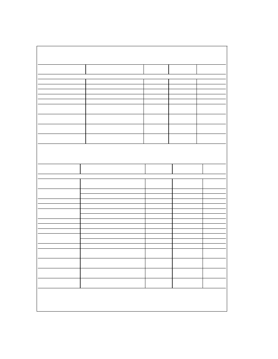
Electrical Characteristics
V
IN
= 14V, I
stby
= 1 mA, C
stby
= 10 µF, unless otherwise indicated. Boldface type refers to limits over the entire operating tem-
perature range, -40∞C
T
A
+125∞C, all other limits are for T
A
= T
j
= 25∞C (Note 8) .
Parameter
Conditions
Typical
Limit
Units
(Note 4)
V
standby
(Pin 9)
Output Voltage
1 mA
I
O
7.5 mA
5.00
4.85/4.75
V
min
6V
V
IN
26V
5.15/5.25
V
max
Line Regulation
9V
V
IN
16V
2
25/25
mV
max
7V
V
IN
26V
5
50/50
mV
max
Load Regulation
0.5 mA
I
OUT
7.5 mA
6
50/50
mV
max
Output Impedance
5 mA
dc
and 1 mA
rms
, f
o
= 120 Hz
0.9
Quiescent Current
I
stby
= 7.5 mA
1.2
2.0/4.0
mA
max
I
stby
= 2 mA
0.9
1.5/4.0
mA
max
Output Noise Voltage
10 Hz≠100 kHz, I
stby
= 1 mA
100
µV
Long Term Stability
20
mV/1000 hr
Ripple Rejection
f
o
= 120 Hz
70
60/50
dB
min
Dropout Voltage
I
stby
= 1 mA
0.26
0.50/0.60
V
max
I
stby
= 7.5 mA
0.38
0.60/0.70
V
max
Current Limit
15
12/12
mA
min
Maximum Operational
4.5V
V
stby
6V,
65
60/60
V
min
Input Voltage
R
stby
= 1000
Maximum Line
V
stby
6V, T
100 ms,
65
60/60
V
min
Transient
R
stby
= 1000
Reverse Polarity
V
stby
-0.6V,
-30
-15/-15
V
min
Input Voltage DC
R
stby
= 1000
Reverse Polarity Input
T
100 ms, R
stby
= 1000
-55
-35/-35
V
min
Voltage Transient
3
www.national.com
Electrical Characteristics
V
IN
= 14V, C
OUT
= 10 µF, C
buf
= 10 µF, C
stby
= 10 µF, unless otherwise indicated. Boldface type refers to limits over the en-
tire operating temperature range, -40∞C
T
A
+125∞C, all other limits are for T
A
= T
j
= 25∞C (Note 8) .
Parameter
Conditions
Typical
Limit
Units
(Note 4)
Tracking and Isolation
Tracking
I
OUT
500 mA, I
buf
= 5 mA,
±
30
±
100/
±
100
mV
max
V
OUT
≠V
stby
I
stby
7.5 mA
Tracking
I
OUT
= 5 mA, I
buf
100 mA,
±
30
±
100/
±
100
mV
max
V
buf
≠V
stby
I
stby
7.5 mA
Tracking
I
OUT
500 mA, I
buf
100 mA,
±
30
±
100/
±
100
mV
max
V
OUT
≠V
buf
I
stby
= 1 mA
Isolation (Note 1)
R
OUT
= 1
, I
buf
100 mA
5.00
4.50/4.50
V
min
V
buf
from V
OUT
5.50/5.50
V
max
Isolation (Note 1)
R
OUT
= 1
, I
stby
7.5 mA
5.00
4.50/4.50
V
min
V
stby
from V
OUT
5.50/5.50
V
max
Isolation (Note 1)
R
buf
= 1
, I
OUT
500 mA
5.00
4.50/4.50
V
min
V
OUT
from V
buf
5.50/5.50
V
max
Isolation (Note 1)
R
buf
= 1
, I
stby
7.5 mA
5.00
4.50/4.50
V
min
V
stby
from V
buf
5.50/5.50
V
max
Note 1: Isolation refers to the ability of the specified output to remain within the tested limits when the other output is shorted to ground.
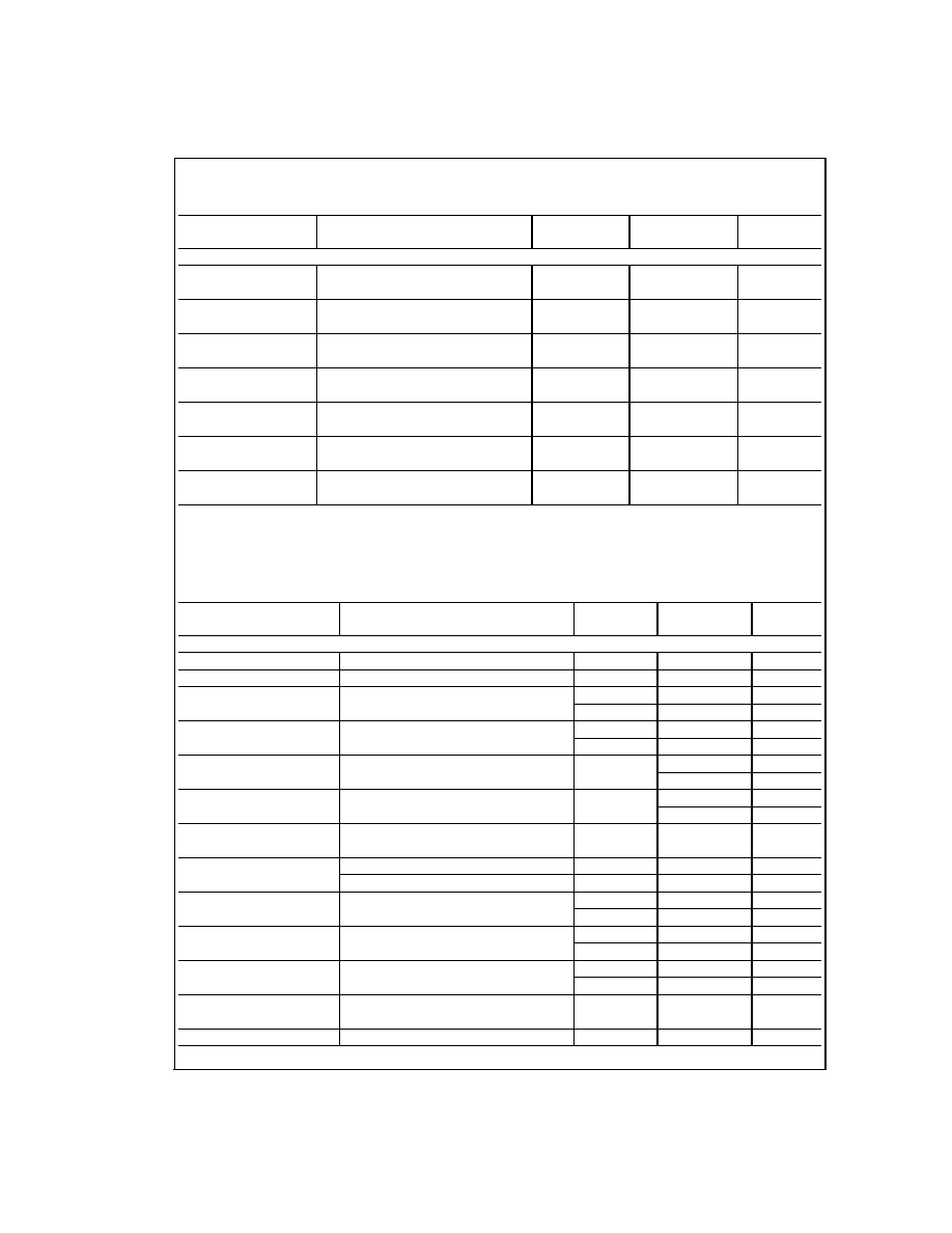
Electrical Characteristics
V
IN
= 14V, I
OUT
= 5 mA, I
buf
= 5 mA, I
stby
= 5 mA, R
t
= 130 k
, C
t
= 0.33 µF, C
mon
= 0.47 µF, unless otherwise indicated,
Boldface type refers to limits over the entire operating temperature range, -40∞C
T
A
+125∞C, all other limits are for T
A
= T
J
= 25∞C (Note 8)
Parameter
Conditions
Typical
Limit
Units
(Note 4)
Computer Monitor/Reset Functions
I
reset
Low
V
IN
= 4V, V
rst
= 0.4V
5
2/0.50
mA
min
V
reset
Low
V
IN
= 4V, I
rst
= 1 mA
0.10
0.40/0.40
V
max
R
t voltage
(Pin 2)
1.22
1.15/0.75
V
min
1.22
1.30/2.00
V
max
Power On Reset
VµP
mon
= 5V
50
45/17.0
ms
min
Delay
(T
dly
= 1.2 R
t
C
t
)
50
55/80.0
ms
max
V
OUT
Low
(Note 6)
-350
-225/-175
mV
min
Reset Threshold
-500/-550
mV
max
V
OUT
High
(Note 6)
600
225/175
mV
min
Reset Threshold
750/800
mV
max
Reset Output
VµP
mon
= 5V, V
rst
= 12V
0.01
1/5.0
µA
max
Leakage
µP
mon
Input Current (Pin 4)
VµP
mon
= 2.4V
7.5
25/25
µA
max
VµP
mon
= 0.4V
0.01
10/15
µA
max
µP
mon
Input
1.22
0.80/0.80
V
min
Threshold Voltage
1.22
2.00/2.00
V
max
µP Monitor Reset
VµP
mon
= 0V
50
45/30
ms
min
Oscillator Period
(T
window
= 0.82 R
t
C
mon
)
50
55/70
ms
max
µP Monitor Reset
VµP
mon
= 0V
1.0
0.7/0.4
ms
min
Oscillator Pulse Width
(RESET
pw
= 2000 C
mon
)
1.0
1.3/2.10
ms
max
Minimum µP Monitor
(Note 7)
2
µs
Input Pulse Width
Reset Fall Time
R
rst
= 10k, V
rst
= 5V, C
rst
10 pF
0.20
1.00/1.00
µs
max
www.national.com
4
Electrical Characteristics
(Continued)
V
IN
= 14V, I
OUT
= 5 mA, I
buf
= 5 mA, I
stby
= 5 mA, R
t
= 130 k
, C
t
= 0.33 µF, C
mon
= 0.47 µF, unless otherwise indicated,
Boldface type refers to limits over the entire operating temperature range, -40∞C
T
A
+125∞C, all other limits are for T
A
= T
J
= 25∞C (Note 8)
Parameter
Conditions
Typical
Limit
Units
(Note 4)
Computer Monitor/Reset Functions
Reset Rise Time
R
rst
= 10k, V
rst
= 5V, C
rst
10 pF
0.60
1.00/1.50
µs
max
On/Off Switch Input
V
ON
= 2.4V
7.5
25/25
µA
max
Current (Pin 8)
V
ON
= 0.4V
0.01
10/10
µA
max
On/Off Switch Input
1.22
0.80/0.80
V
min
Threshold Voltage
1.22
2.00/2.00
V
max
Note 2: Absolute Maximum Ratings indicate limits beyond which damage to the device may occur. DC and AC electrical specifications do not apply when operating
the device beyond its specified operating ratings.
Note 3: Thermal resistance without a heatsink for junction-to-case temperature is 3∞C/W. Thermal resistance case-to-ambient is 40∞C/W.
Note 4: Tested Limits are guaranteed and 100% production tested.
Note 5: Human body model, 100 pF capacitor discharged through a 1500
resistor.
Note 6: Internal comparators detect when the main regulator output (V
OUT
) changes from the measured output voltage (with V
IN
= 14V) by the specified amount,
V
OUT
High or
V
OUT
Low, and set the Reset Error Flag low. The Reset Error Flag is held low until V
OUT
returns to regulation. The Reset Error Flag is then allowed
to go high again after a delay set by R
t
and C
t
. (see application section).
Note 7: This parameter is a measure of how short a pulse can be detected at the µP Monitor Input. This parameter is primarily influenced by the value of C
mon
. (See
Application Hints Section.)
Note 8: To ensure constant junction temperature, low duty cycle pulse testing is used.
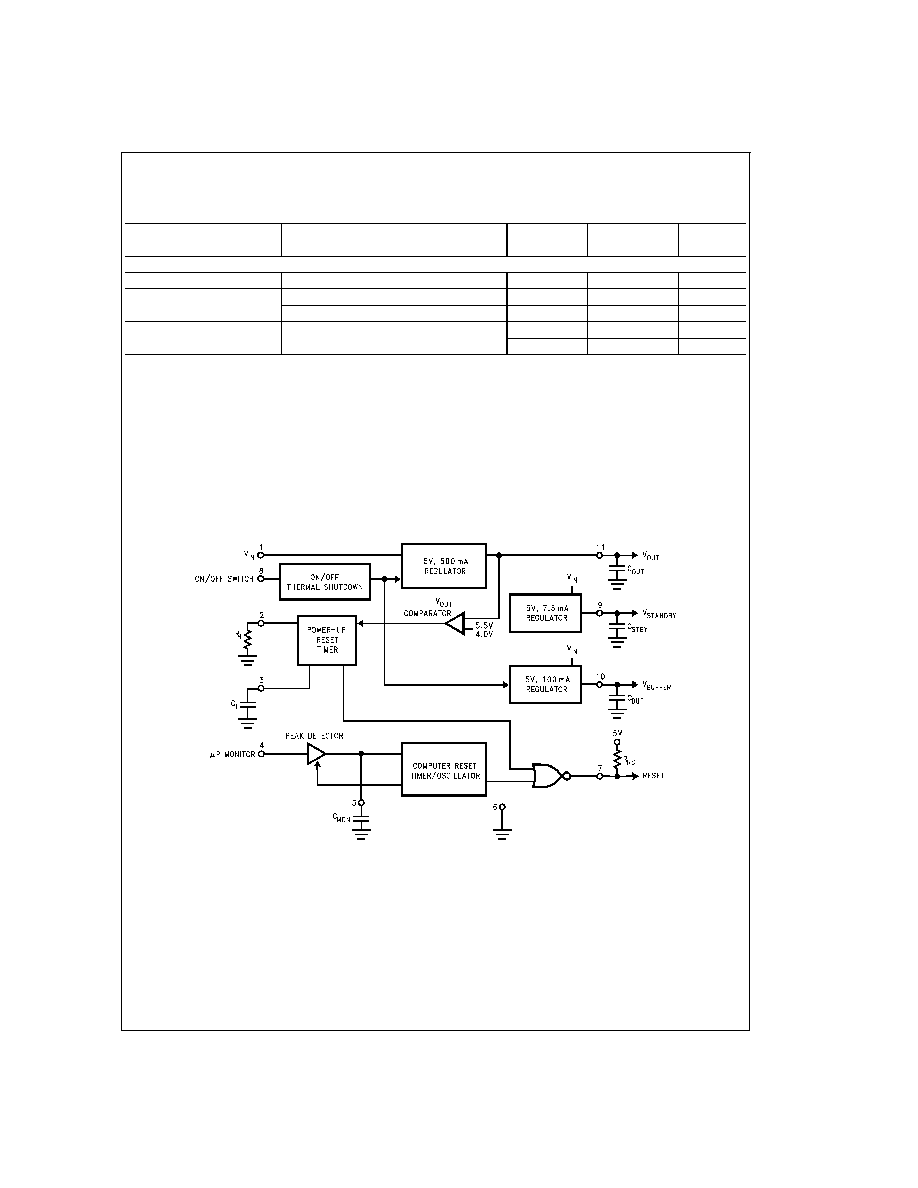
Block Diagram
DS011252-2
5
www.national.com