
LM2991
Negative Low Dropout Adjustable Regulator
General Description
The LM2991 is a low dropout adjustable negative regulator
with a output voltage range between -3V to -24V. The
LM2991 provides up to 1A of load current and features a On
/Off pin for remote shutdown capability.
The LM2991 uses new circuit design techniques to provide a
low dropout voltage, low quiescent current and low tempera-
ture coefficient precision reference. The dropout voltage at
1A load current is typically 0.6V and a guaranteed
worst-case maximum of 1V over the entire operating tem-
perature range. The quiescent current is typically 1 mA with
a 1A load current and an input-output voltage differential
greater than 3V. A unique circuit design of the internal bias
supply limits the quiescent current to only 9 mA (typical)
when the regulator is in the dropout mode (V
OUT
- V
IN
3V).
The LM2991 is short-circuit proof, and thermal shutdown in-
cludes hysteresis to enhance the reliability of the device
when inadvertently overloaded for extended periods. The
LM2991 is available in 5-lead TO-220 and TO-263 packages
and is rated for operation over the automotive temperature
range of -40∞C to +125∞C. Mil-Aero versions are also avail-
able.
Features
n
Output voltage adjustable from -3V to -24V, typically
-2V to -25V
n
Output current in excess of 1A
n
Dropout voltage typically 0.6V at 1A load
n
Low quiescent current
n
Internal short circuit current limit
n
Internal thermal shutdown with hysteresis
n
TTL, CMOS compatible ON/OFF switch
n
Functional complement to the LM2941 series
Applications
n
Post switcher regulator
n
Local, on-card, regulation
n
Battery operated equipment
Typical Application
DS011260-1
V
OUT
= V
REF
(1 + R2/R1)
*Required if the regulator is located further than 6 inches from the power supply filter capacitors. A 1 µF solid tantalum or a 10 µF aluminum electrolytic
capacitor is recommended.
*
*Required for stability. Must be at least a 10 µF aluminum electrolytic or a 1 µF solid tantalum to maintain stability. May be increased without bound to
maintain regulation during transients. Locate the capacitor as close as possible to the regulator. The equivalent series resistance (ESR) is critical, and
should be less than 10
over the same operating temperature range as the regulator.
September 2000
LM2991
Negative
Low
Dropout
Adjustable
Regulator
© 2000 National Semiconductor Corporation
DS011260
www.national.com
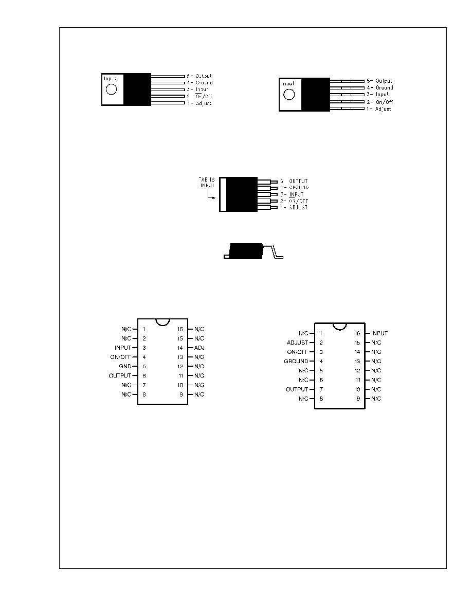
Connection Diagrams and Ordering Information
5-Lead TO-220
Straight Leads
DS011260-9
Front View
Order Number LM2991T
See NS Package Number T05A
5-Lead TO-220
Bent, Staggered Leads
DS011260-2
Front View
Order Number LM2991T Flow LB03
See NS Package Number T05D
TO263
5-Lead Surface-Mount Package
DS011260-11
Top View
DS011260-12
Side View
Order Number LM2991S
See NS Package Number TS5B
16-Lead Ceramic Dual-in-Line Package
DS011260-29
Top View
Order Number LM2991J-QMLV
5962-9650501VEA
Order Number LM2991J-QML
5962-9650501QEA
See NS Package Number J16A
16-Lead Ceramic Surface-Mount Package
DS011260-30
Top View
Order Number LM2991WG-QML
5962-9650501QXA
See NS Package Number WG16A
LM2991
www.national.com
2
Absolute Maximum Ratings
(Note 1)
If Military/Aerospace specified devices are required,
please contact the National Semiconductor Sales Office/
Distributors for availability and specifications.
Input Voltage
-26V to +0.3V
ESD Susceptibility (Note 2)
2 kV
Power Dissipation (Note 3)
Internally limited
Junction Temperature (T
Jmax
)
125∞C
Storage Temperature Range
-65∞C to +150∞C
Lead Temperature (Soldering, 10 sec.)
230∞C
Operating Ratings
(Note 1)
Junction Temperature Range (T
J
)
-40∞C to +125∞C
Maximum Input Voltage (Operational)
-26V
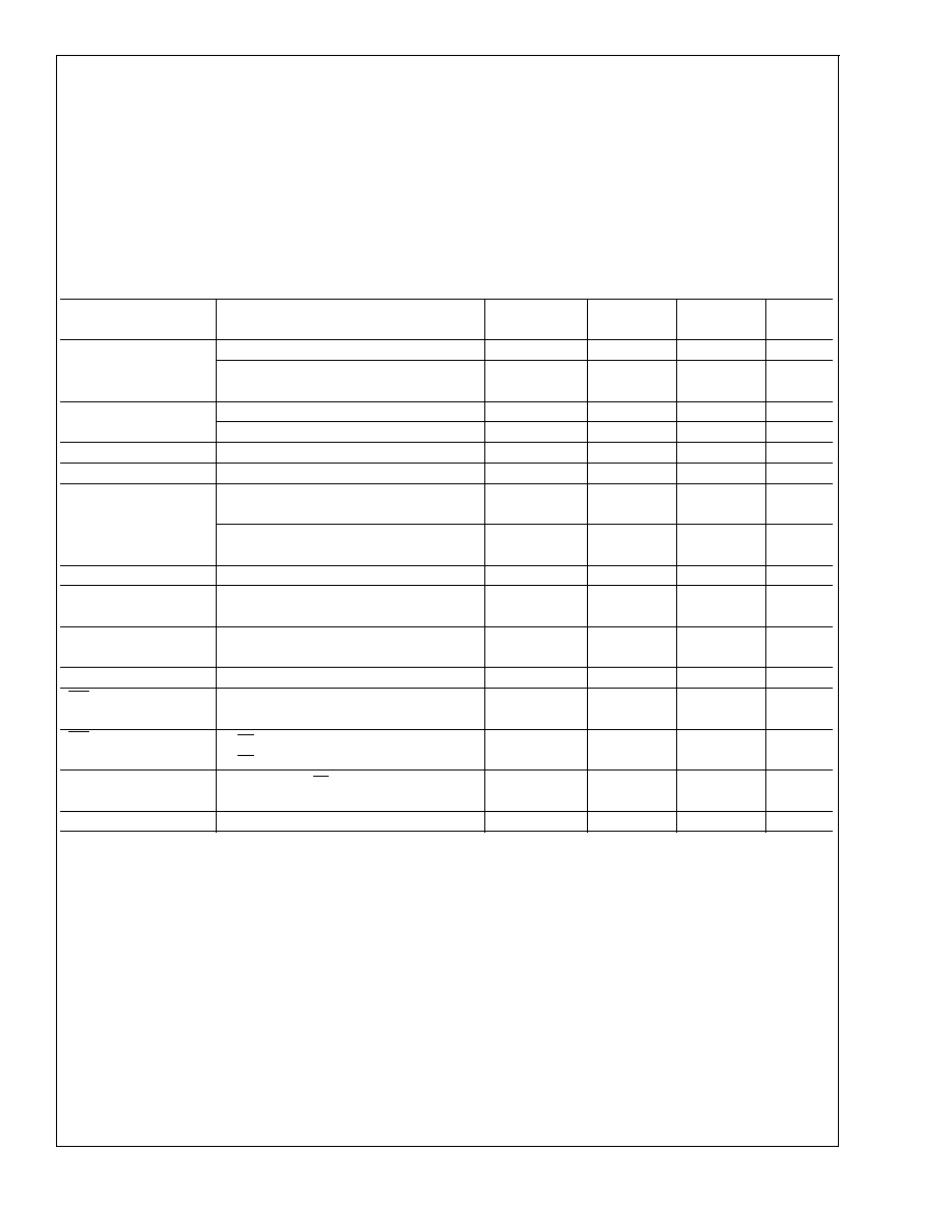
Electrical Characteristics
V
IN
= -10V, V
O
= -3V, I
O
= 1A, C
O
= 47 µF, R1 = 2.7k, T
J
= 25∞C, unless otherwise specified. Boldface limits apply over
the entire operating junction temperature range.
Parameter
Conditions
Typical
Min
Max
Units
(Note 4)
Reference Voltage
5 mA
I
O
1A
-1.210
-1.234
-1.186
V
5 mA
I
O
1A,
-1.27
-1.15
V
V
O
- 1V
V
IN
-26V
Output Voltage
-2
-3
V
Range
V
IN
= -26V
-25
-24
V
Line Regulation
I
O
= 5 mA, V
O
- 1V
V
IN
-26V
0.004
0.04
%/V
Load Regulation
50 mA
I
O
1A
0.04
0.4
%
Dropout Voltage
I
O
= 0.1A,
V
O
100 mV
0.1
0.2
V
0.3
I
O
= 1A,
V
O
100 mV
0.6
0.8
V
1
Quiescent Current
I
O
1A
0.7
5
mA
Dropout Quiescent
V
IN
= V
O
, I
O
1A
16
50
mA
Current
Ripple Rejection
V
ripple
= 1 Vrms,
f
ripple
= 1 kHz,
60
50
dB
I
O
= 5 mA
Output Noise
10 Hz - 100 kHz, I
O
= 5 mA
200
450
µV
ON /OFF Input
(V
OUT
: ON)
1.2
0.8
V
Voltage
(V
OUT
: OFF)
1.3
2.4
ON /OFF Input
V
ON/OFF
= 0.8V (V
OUT
: ON)
0.1
10
µA
Current
V
ON/OFF
= 2.4V (V
OUT
: OFF)
40
100
Output Leakage
V
IN
= -26V, V
ON/OFF
= 2.4V
60
250
µA
Current
V
OUT
= 0V
Current Limit
V
OUT
= 0V
2
1.5
A
Note 1: Absolute Maximum Ratings indicate limits beyond which damage to the device may occur. Operating Ratings indicate conditions for which the deivce is in-
tended to be functional, but do not guarantee specific performance limits. For guaranteed specifications and test conditions, see the Electrical Characteristics.
Note 2: Human body model, 100 pF discharged through a 1.5 k
resistor.
Note 3: The maximum power dissipation is a function of T
Jmax
,
JA
and T
A
. The maximum allowable power dissipation at any ambient temperature is P
D
= (T
Jmax
- T
A
)/
JA
. If this dissipation is exceeded, the die temperature will rise above 125∞C and the LM2991 will go into thermal shutdown. For the LM2991, the
junction-to-ambient thermal resistance is 53∞C/W for the TO-220, 73∞C/W for the TO-263, and junction-to-case thermal resistance is 3∞C. If the TO-263 package is
used, the thermal resistance can be reduced by increasing the PC board copper area thermally connected to the package. Using 0.5 square inches of copper area,
JA
is 50∞C/W; with 1 square inch of copper area,
JA
is 37∞C/W; and with 1.6 or more square inches of copper area,
JA
is 32∞C/W.
Note 4: Typicals are at T
J
= 25∞C and represent the most likely parametric norm.
LM2991
www.national.com
3
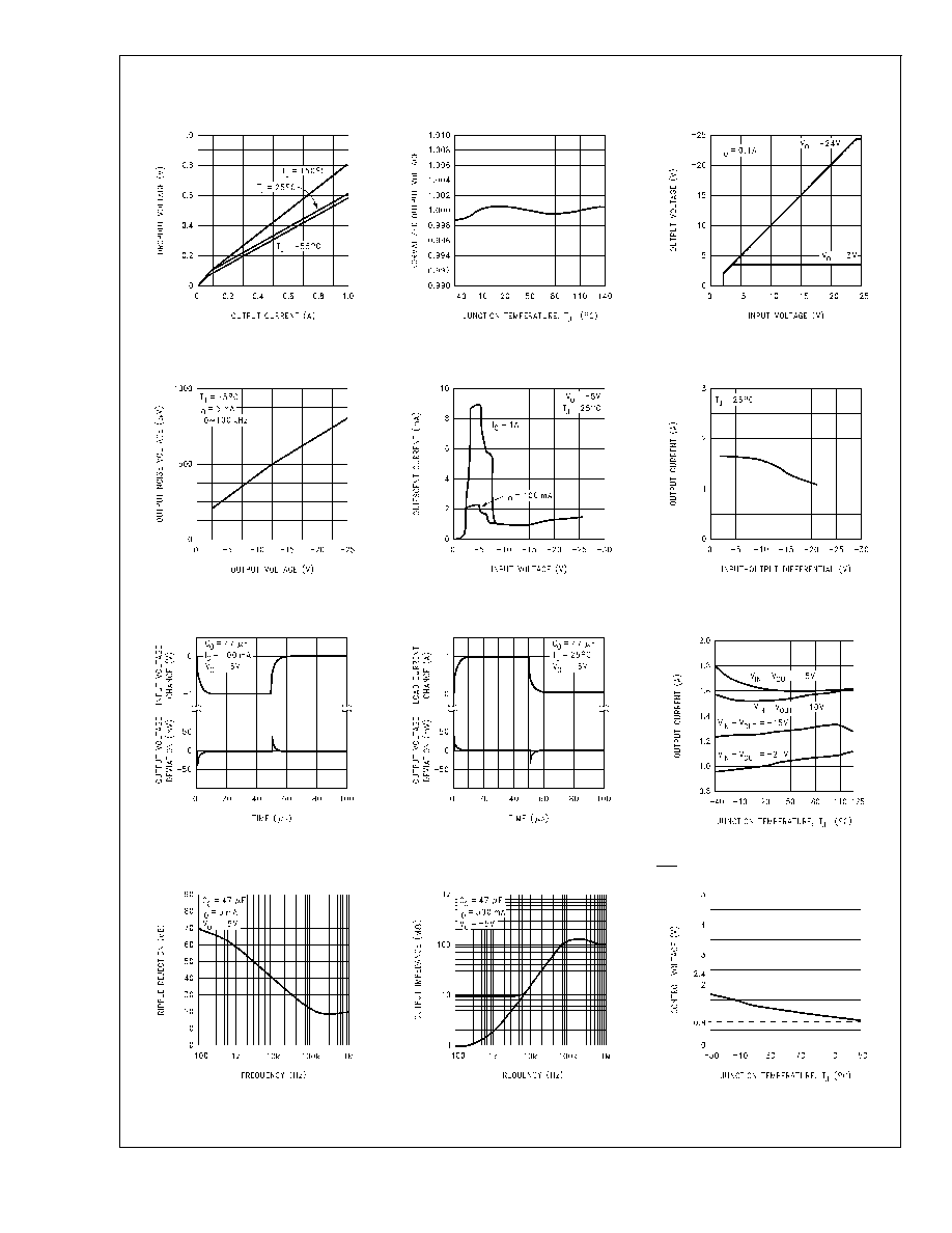
Typical Performance Characteristics
Dropout Voltage
DS011260-13
Normalized Output Voltage
DS011260-14
Output Voltage
DS011260-15
Output Noise Voltage
DS011260-16
Quiescent Current
DS011260-17
Maximum Output Current
DS011260-18
Line Transient Response
DS011260-19
Load Transient Response
DS011260-20
Maximum Output Current
DS011260-21
Ripple Rejection
DS011260-22
Output Impedance
DS011260-23
ON /OFF Control Voltage
DS011260-24
LM2991
www.national.com
4
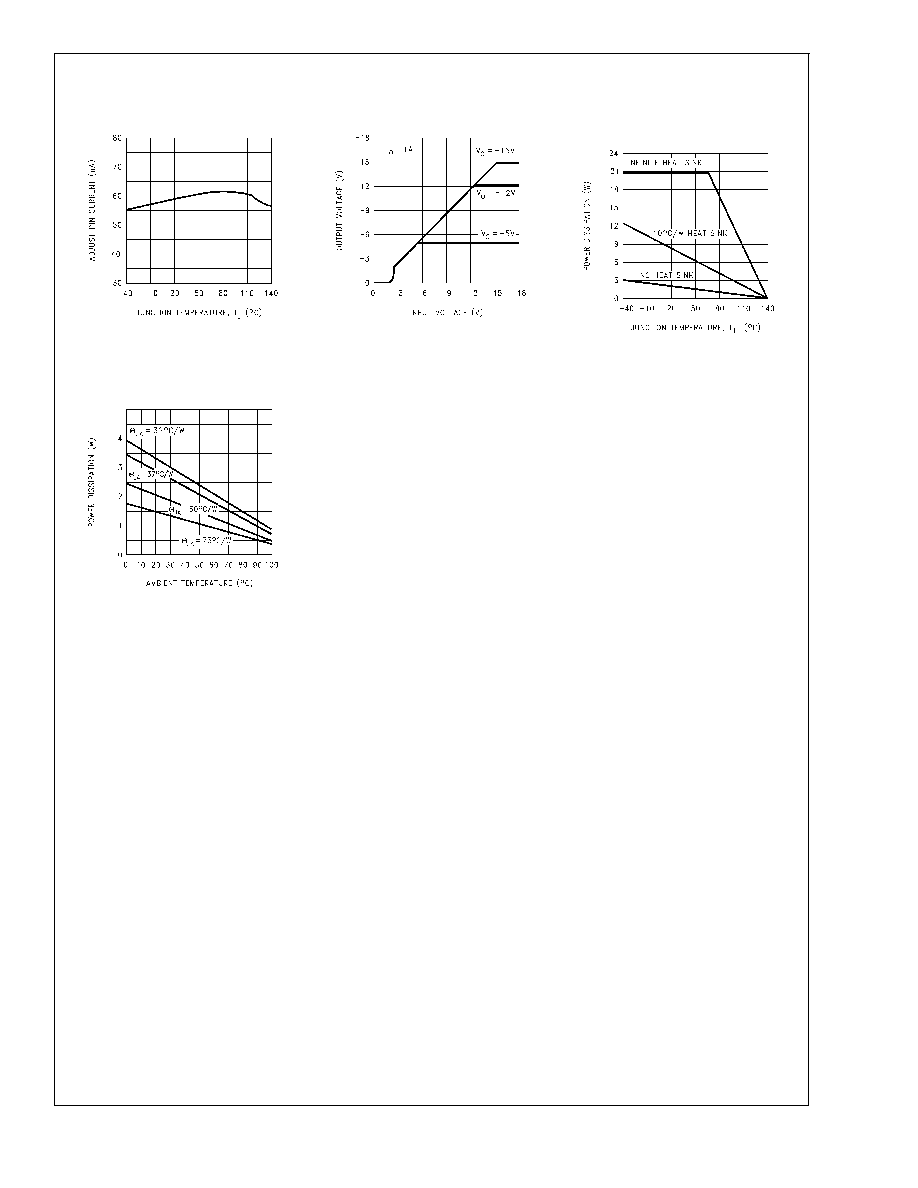
Typical Performance Characteristics
(Continued)
Application Hints
External Capacitors
Like any low-dropout regulator, external capacitors are re-
qired to stabilize the control loop. These capacitors must be
correctly selected for proper performance.
INPUT CAPACITOR: An input capacitor is reqiuired if the
regulator is located more than 6
from the input power supply
filter capacitor (or if no other input capaciotr is present).
A solid Tantalum or ceramic capacitor whose value is at least
1 µF is recommended, but an aluminum electrolytic (
10 µF)
may be used. However, aluminum electrolytics should not be
used in applications where the ambient temperature can
drop below 0∞C because their internal impedance increases
significantly at cold temperatures.
OUTPUT CAPACITOR: The output capacitor must meet the
ESR limits shown in the graph, which means it must have an
ESR between about 25 m
and 10
.
A solid Tantalum (value
1 µF) is the best choice for the out-
put capacitor. An aluminum electrolytic (
10 µF) may be
used if the ESR is in the stable range.
It should be noted that the ESR of a typical aluminum elec-
trolytic will increase by as much as 50X as the temperature
is reduced from 25∞C down to -40∞C, while a Tantalum will
exhibit an ESR increase of about 2X over the same range.
For this and other reasons, aluminum electrolytics should
not be used in applications where low operating tempera-
tures occur.
The lower stable ESR limit of 25 m
means that ceramic ca-
pacitors can not be used directly on the output of an LDO. A
ceramic (
2.2 µF) can be used on the output if some exter-
nal resistance is placed in series with it (1
recommended).
Dielectric types X7R or X5R must be used if the temperature
range of the application varies more than
±
25∞ from ambient
to assure the amount of capacitance is sufficient.
CERAMIC BYPASS CAPACITORS:Many designers place
distributed ceramic capacitors whose value is in the range of
1000 pF to 0.1 µF at the power input pins of the IC's across
a circuit board. These can cause reduced phase margin or
oscillations in LDO regulators.
The advent of multi-layer boards with dedicated power and
ground planes has removed the trace inductance that (previ-
ously) provided the necessary
decoupling
to shield the out-
put of the LDO from the effects of bypass capacitors.
These capacitors should be avoided if possible, and kept as
far far away from the LDO output as is practical.
Adjust Pin Current
DS011260-25
Low Voltage Behavior
DS011260-26
Maximum Power
Dissipation (TO-220)
DS011260-27
Maximum Power Dissipation
(TO-263) (See Note 3)
DS011260-28
LM2991
www.national.com
5