 | –≠–ª–µ–∫—Ç—Ä–æ–Ω–Ω—ã–π –∫–æ–º–ø–æ–Ω–µ–Ω—Ç: LM317AMDC | –°–∫–∞—á–∞—Ç—å:  PDF PDF  ZIP ZIP |
LM117/LM317A/LM317
3-Terminal Adjustable Regulator
General Description
The LM117 series of adjustable 3-terminal positive voltage
regulators is capable of supplying in excess of 1.5A over a
1.2V to 37V output range. They are exceptionally easy to
use and require only two external resistors to set the output
voltage. Further, both line and load regulation are better than
standard fixed regulators. Also, the LM117 is packaged in
standard transistor packages which are easily mounted and
handled.
In addition to higher performance than fixed regulators, the
LM117 series offers full overload protection available only in
IC's. Included on the chip are current limit, thermal overload
protection and safe area protection. All overload protection
circuitry remains fully functional even if the adjustment ter-
minal is disconnected.
Normally, no capacitors are needed unless the device is
situated more than 6 inches from the input filter capacitors in
which case an input bypass is needed. An optional output
capacitor can be added to improve transient response. The
adjustment terminal can be bypassed to achieve very high
ripple rejection ratios which are difficult to achieve with stan-
dard 3-terminal regulators.
Besides replacing fixed regulators, the LM117 is useful in a
wide variety of other applications. Since the regulator is
"floating" and sees only the input-to-output differential volt-
age, supplies of several hundred volts can be regulated as
long as the maximum input to output differential is not ex-
ceeded, i.e., avoid short-circuiting the output.
Also, it makes an especially simple adjustable switching
regulator, a programmable output regulator, or by connecting
a fixed resistor between the adjustment pin and output, the
LM117 can be used as a precision current regulator. Sup-
plies with electronic shutdown can be achieved by clamping
the adjustment terminal to ground which programs the out-
put to 1.2V where most loads draw little current.
For applications requiring greater output current, see LM150
series (3A) and LM138 series (5A) data sheets. For the
negative complement, see LM137 series data sheet.
Features
n
Guaranteed 1% output voltage tolerance (LM317A)
n
Guaranteed max. 0.01%/V line regulation (LM317A)
n
Guaranteed max. 0.3% load regulation (LM117)
n
Guaranteed 1.5A output current
n
Adjustable output down to 1.2V
n
Current limit constant with temperature
n
P
+
Product Enhancement tested
n
80 dB ripple rejection
n
Output is short-circuit protected
Typical Applications
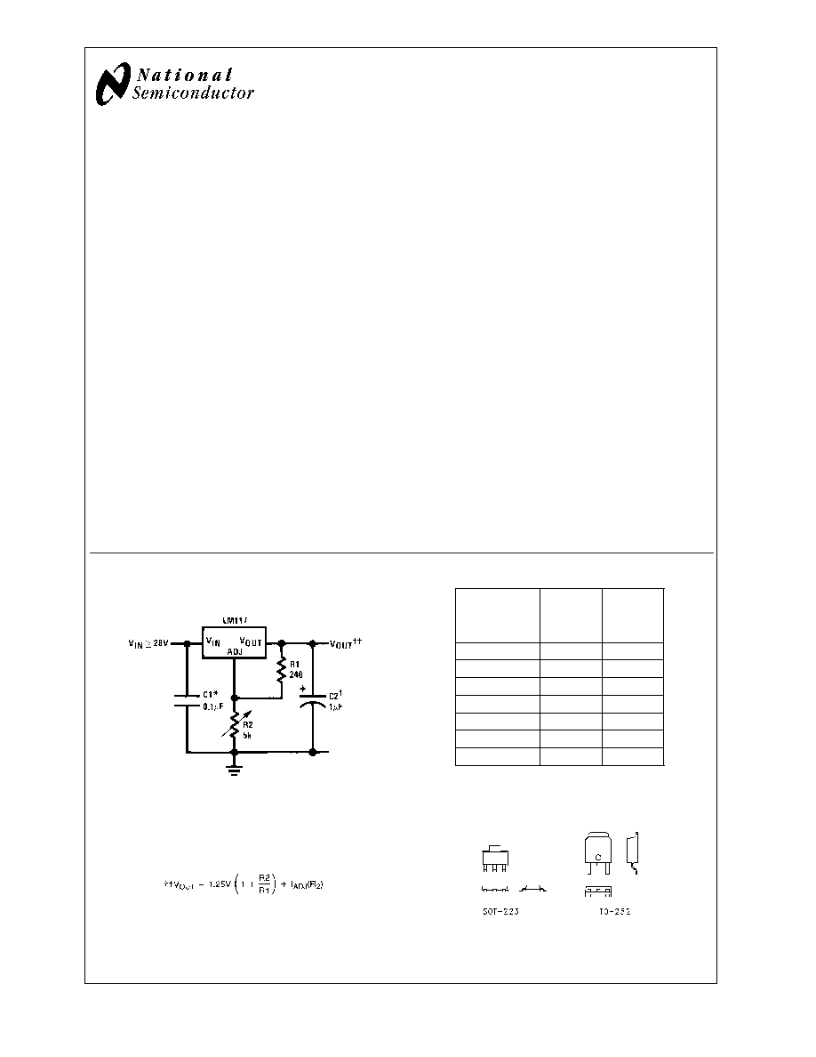
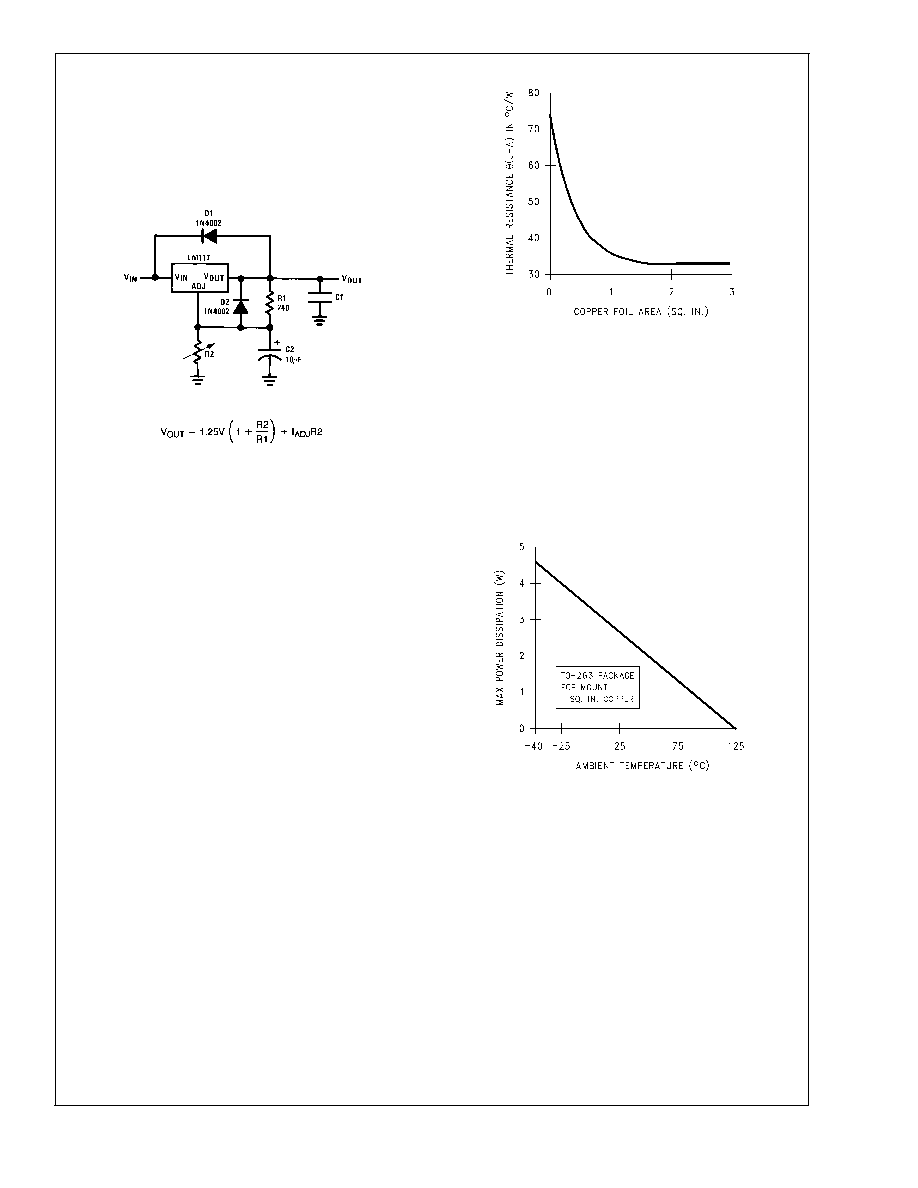
1.2V≠25V Adjustable Regulator
00906301
Full output current not available at high input-output voltages
*Needed if device is more than 6 inches from filter capacitors.
Optional -- improves transient response. Output capacitors in the range
of 1 µF to 1000 µF of aluminum or tantalum electrolytic are commonly
used to provide improved output impedance and rejection of transients.
LM117 Series Packages
Part Number
Design
Suffix
Package
Load
Current
K
TO-3
1.5A
H
TO-39
0.5A
T
TO-220
1.5A
E
LCC
0.5A
S
TO-263
1.5A
EMP
SOT-223
1A
MDT
TO-252
0.5A
SOT-223 vs D-Pak (TO-252)
Packages
00906354
Scale 1:1
September 2002
LM1
17/LM317A/LM317
3-T
erminal
Adjustable
Regulator
© 2002 National Semiconductor Corporation
DS009063
www.national.com
Absolute Maximum Ratings
(Note 1)
If Military/Aerospace specified devices are required,
please contact the National Semiconductor Sales Office/
Distributors for availability and specifications.
Power Dissipation
Internally Limited
Input-Output Voltage Differential
+40V, -0.3V
Storage Temperature
-65∞C to +150∞C
Lead Temperature
Metal Package (Soldering, 10 seconds)
300∞C
Plastic Package (Soldering, 4 seconds)
260∞C
ESD Tolerance (Note 5)
3 kV
Operating Temperature Range
LM117
-55∞C
T
J
+150∞C
LM317A
-40∞C
T
J
+125∞C
LM317
0∞C
T
J
+125∞C
Preconditioning
Thermal Limit Burn-In
All Devices 100%
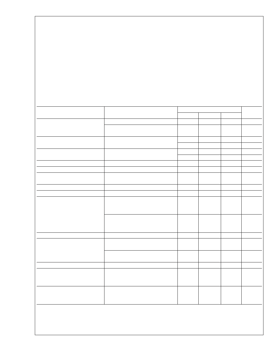
Electrical Characteristics
(Note 3)
Specifications with standard type face are for T
J
= 25∞C, and those with boldface type apply over full Operating Tempera-
ture Range. Unless otherwise specified, V
IN
- V
OUT
= 5V, and I
OUT
= 10 mA.
Parameter
Conditions
LM117 (Note 2)
Units
Min
Typ
Max
Reference Voltage
V
3V
(V
IN
- V
OUT
)
40V,
1.20
1.25
1.30
V
10 mA
I
OUT
I
MAX
, P
P
MAX
Line Regulation
3V
(V
IN
- V
OUT
)
40V (Note 4)
0.01
0.02
%/V
0.02
0.05
%/V
Load Regulation
10 mA
I
OUT
I
MAX
(Note 4)
0.1
0.3
%
0.3
1
%
Thermal Regulation
20 ms Pulse
0.03
0.07
%/W
Adjustment Pin Current
50
100
µA
Adjustment Pin Current Change
10 mA
I
OUT
I
MAX
0.2
5
µA
3V
(V
IN
- V
OUT
)
40V
Temperature Stability
T
MIN
T
J
T
MAX
1
%
Minimum Load Current
(V
IN
- V
OUT
) = 40V
3.5
5
mA
Current Limit
(V
IN
- V
OUT
)
15V
K Package
1.5
2.2
3.4
A
H Packages
0.5
0.8
1.8
A
(V
IN
- V
OUT
) = 40V
K Package
0.3
0.4
A
H Package
0.15
0.2
A
RMS Output Noise, % of V
OUT
10 Hz
f 10 kHz
0.003
%
Ripple Rejection Ratio
V
OUT
= 10V, f = 120 Hz,
65
dB
C
ADJ
= 0 µF
V
OUT
= 10V, f = 120 Hz,
66
80
dB
C
ADJ
= 10 µF
Long-Term Stability
T
J
= 125∞C, 1000 hrs
0.3
1
%
Thermal Resistance,
K Package
2.3
3
∞C/W
Junction-to-Case
H Package
12
15
∞C/W
E Package
∞C/W
Thermal Resistance, Junction-
K Package
35
∞C/W
to-Ambient (No Heat Sink)
H Package
140
∞C/W
E Package
∞C/W
LM1
17/LM317A/LM317
www.national.com
2
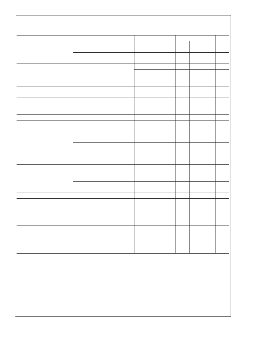
Electrical Characteristics
(Note 3)
Specifications with standard type face are for T
J
= 25∞C, and those with boldface type apply over full Operating Tempera-
ture Range. Unless otherwise specified, V
IN
- V
OUT
= 5V, and I
OUT
= 10 mA.
Parameter
Conditions
LM317A
LM317
Units
Min
Typ
Max
Min
Typ
Max
Reference Voltage
1.238
1.250
1.262
V
3V
(V
IN
- V
OUT
)
40V,
1.225
1.250
1.270
1.20
1.25
1.30
V
10 mA
I
OUT
I
MAX
, P
P
MAX
Line Regulation
3V
(V
IN
- V
OUT
)
40V (Note 4)
0.005
0.01
0.01
0.04
%/V
0.01
0.02
0.02
0.07
%/V
Load Regulation
10 mA
I
OUT
I
MAX
(Note 4)
0.1
0.5
0.1
0.5
%
0.3
1
0.3
1.5
%
Thermal Regulation
20 ms Pulse
0.04
0.07
0.04
0.07
%/W
Adjustment Pin Current
50
100
50
100
µA
Adjustment Pin Current
Change
10 mA
I
OUT
I
MAX
0.2
5
0.2
5
µA
3V
(V
IN
- V
OUT
)
40V
Temperature Stability
T
MIN
T
J
T
MAX
1
1
%
Minimum Load Current
(V
IN
- V
OUT
) = 40V
3.5
10
3.5
10
mA
Current Limit
(V
IN
- V
OUT
)
15V
K, T, S Packages
1.5
2.2
3.4
1.5
2.2
3.4
A
H Package
MP Package
0.5
1.5
0.8
2.2
1.8
3.4
0.5
1.5
0.8
2.2
1.8
3.4
A
A
(V
IN
- V
OUT
) = 40V
K, T, S Packages
0.15
0.4
0.15
0.4
A
H Package
MP Package
0.075
0.55
0.2
0.4
0.075
0.15
0.2
0.4
A
A
RMS Output Noise, % of V
OUT
10 Hz
f 10 kHz
0.003
0.003
%
Ripple Rejection Ratio
V
OUT
= 10V, f = 120 Hz,
65
65
dB
C
ADJ
= 0 µF
V
OUT
= 10V, f = 120 Hz,
66
80
66
80
dB
C
ADJ
= 10 µF
Long-Term Stability
T
J
= 125∞C, 1000 hrs
0.3
1
0.3
1
%
Thermal Resistance,
Junction-to-Case
K Package
MDT Package
2.3
5
3
∞C/W
∞C/W
H Package
12
15
12
15
∞C/W
T Package
MP Package
4
23.5
5
4
23.5
∞C/W
∞C/W
Thermal Resistance,
Junction-to-Ambient (No Heat
Sink)
K Package
MDT Package(Note 6)
35
35
92
∞C/W
∞C/W
H Package
140
140
∞C/W
T Package
50
50
∞C/W
S Package (Note 6)
50
50
∞C/W
Note 1: Absolute Maximum Ratings indicate limits beyond which damage to the device may occur. Operating Ratings indicate conditions for which the device is
intended to be functional, but do not guarantee specific performance limits. For guaranteed specifications and test conditions, see the Electrical Characteristics. The
guaranteed specifications apply only for the test conditions listed.
Note 2: Refer to RETS117H drawing for the LM117H, or the RETS117K for the LM117K military specifications.
Note 3: Although power dissipation is internally limited, these specifications are applicable for maximum power dissipations of 2W for the TO-39 and SOT-223 and
20W for the TO-3, TO-220, and TO-263. I
MAX
is 1.5A for the TO-3, TO-220, and TO-263 packages, 0.5A for the TO-39 package and 1A for the SOT-223 Package.
All limits (i.e., the numbers in the Min. and Max. columns) are guaranteed to National's AOQL (Average Outgoing Quality Level).
Note 4: Regulation is measured at a constant junction temperature, using pulse testing with a low duty cycle. Changes in output voltage due to heating effects are
covered under the specifications for thermal regulation.
Note 5: Human body model, 100 pF discharged through a 1.5 k
resistor.
Note 6: If the TO-263 or TO-252 packages are used, the thermal resistance can be reduced by increasing the PC board copper area thermally connected to the
package. Using 0.5 square inches of copper area.
JA
is 50∞C/W; with 1 square inch of copper area,
JA
is 37∞C/W; and with 1.6 or more square inches of copper
area,
JA
is 32∞C/W. If the SOT-223 package is used, the thermal resistance can be reduced by increasing the PC board copper area (see applications hints for
heatsinking).
LM1
17/LM317A/LM317
www.national.com
3
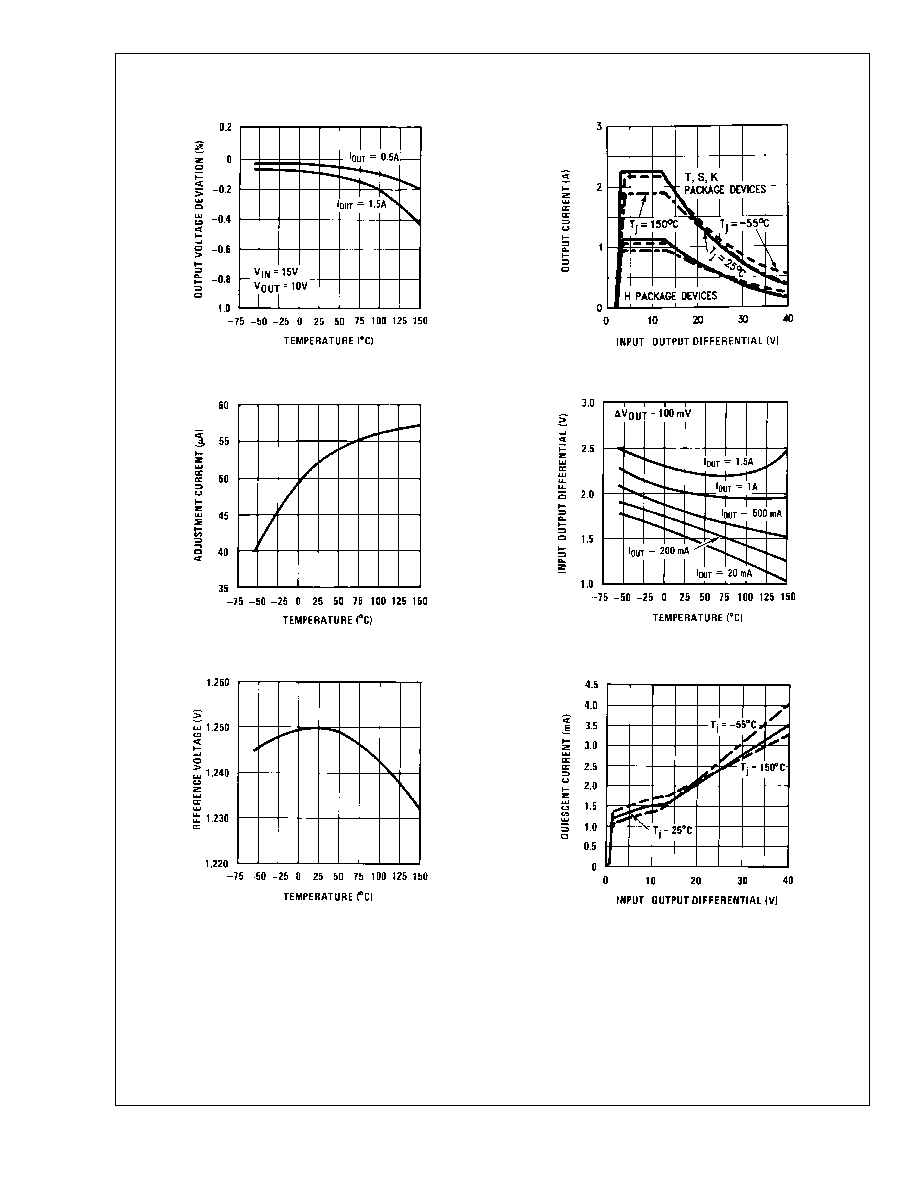
Typical Performance Characteristics
Output Capacitor = 0 µF unless otherwise noted
Load Regulation
Current Limit
00906337
00906338
Adjustment Current
Dropout Voltage
00906339
00906340
Temperature Stability
Minimum Operating Current
00906341
00906342
LM1
17/LM317A/LM317
www.national.com
4
Typical Performance Characteristics
Output Capacitor = 0 µF unless otherwise noted (Continued)
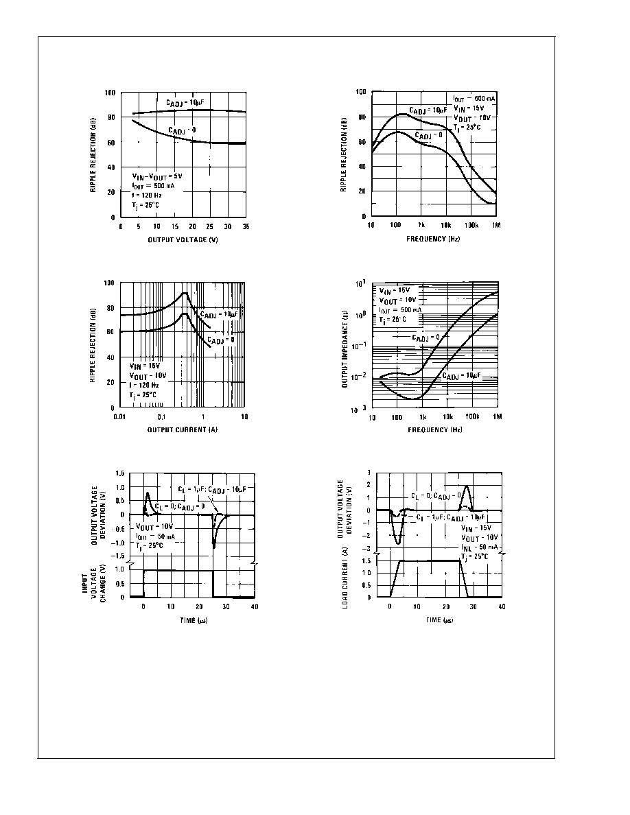
Ripple Rejection
Ripple Rejection
00906343
00906344
Ripple Rejection
Output Impedance
00906345
00906346
Line Transient Response
Load Transient Response
00906347
00906348
LM1
17/LM317A/LM317
www.national.com
5

Application Hints
In operation, the LM117 develops a nominal 1.25V reference
voltage, V
REF
, between the output and adjustment terminal.
The reference voltage is impressed across program resistor
R1 and, since the voltage is constant, a constant current I
1
then flows through the output set resistor R2, giving an
output voltage of
Since the 100 µA current from the adjustment terminal rep-
resents an error term, the LM117 was designed to minimize
I
ADJ
and make it very constant with line and load changes.
To do this, all quiescent operating current is returned to the
output establishing a minimum load current requirement. If
there is insufficient load on the output, the output will rise.
External Capacitors
An input bypass capacitor is recommended. A 0.1 µF disc or
1 µF solid tantalum on the input is suitable input bypassing
for almost all applications. The device is more sensitive to
the absence of input bypassing when adjustment or output
capacitors are used but the above values will eliminate the
possibility of problems.
The adjustment terminal can be bypassed to ground on the
LM117 to improve ripple rejection. This bypass capacitor
prevents ripple from being amplified as the output voltage is
increased. With a 10 µF bypass capacitor 80 dB ripple re-
jection is obtainable at any output level. Increases over
10 µF do not appreciably improve the ripple rejection at
frequencies above 120 Hz. If the bypass capacitor is used, it
is sometimes necessary to include protection diodes to pre-
vent the capacitor from discharging through internal low
current paths and damaging the device.
In general, the best type of capacitors to use is solid tanta-
lum. Solid tantalum capacitors have low impedance even at
high frequencies. Depending upon capacitor construction, it
takes about 25 µF in aluminum electrolytic to equal 1 µF
solid tantalum at high frequencies. Ceramic capacitors are
also good at high frequencies; but some types have a large
decrease in capacitance at frequencies around 0.5 MHz. For
this reason, 0.01 µF disc may seem to work better than a 0.1
µF disc as a bypass.
Although the LM117 is stable with no output capacitors, like
any feedback circuit, certain values of external capacitance
can cause excessive ringing. This occurs with values be-
tween 500 pF and 5000 pF. A 1 µF solid tantalum (or 25 µF
aluminum electrolytic) on the output swamps this effect and
insures stability. Any increase of the load capacitance larger
than 10 µF will merely improve the loop stability and output
impedance.
Load Regulation
The LM117 is capable of providing extremely good load
regulation but a few precautions are needed to obtain maxi-
mum performance. The current set resistor connected be-
tween the adjustment terminal and the output terminal (usu-
ally 240
) should be tied directly to the output (case) of the
regulator rather than near the load. This eliminates line
drops from appearing effectively in series with the reference
and degrading regulation. For example, a 15V regulator with
0.05
resistance between the regulator and load will have a
load regulation due to line resistance of 0.05
x I
L
. If the set
resistor is connected near the load the effective line resis-
tance will be 0.05
(1 + R2/R1) or in this case, 11.5 times
worse.
Figure 2 shows the effect of resistance between the regula-
tor and 240
set resistor.
With the TO-3 package, it is easy to minimize the resistance
from the case to the set resistor, by using two separate leads
to the case. However, with the TO-39 package, care should
be taken to minimize the wire length of the output lead. The
ground of R2 can be returned near the ground of the load to
provide remote ground sensing and improve load regulation.
Protection Diodes
When external capacitors are used with any IC regulator it is
sometimes necessary to add protection diodes to prevent
the capacitors from discharging through low current points
into the regulator. Most 10 µF capacitors have low enough
internal series resistance to deliver 20A spikes when
shorted. Although the surge is short, there is enough energy
to damage parts of the IC.
When an output capacitor is connected to a regulator and
the input is shorted, the output capacitor will discharge into
the output of the regulator. The discharge current depends
on the value of the capacitor, the output voltage of the
regulator, and the rate of decrease of V
IN
. In the LM117, this
discharge path is through a large junction that is able to
sustain 15A surge with no problem. This is not true of other
types of positive regulators. For output capacitors of 25 µF or
less, there is no need to use diodes.
The bypass capacitor on the adjustment terminal can dis-
charge through a low current junction. Discharge occurs
00906305
FIGURE 1.
00906306
FIGURE 2. Regulator with Line Resistance in Output
Lead
LM1
17/LM317A/LM317
www.national.com
6
Application Hints
(Continued)
when either the input or output is shorted. Internal to the
LM117 is a 50
resistor which limits the peak discharge
current. No protection is needed for output voltages of 25V
or less and 10 µF capacitance. Figure 3 shows an LM117
with protection diodes included for use with outputs greater
than 25V and high values of output capacitance.
When a value for
(H-A)
is found using the equation shown,
a heatsink must be selected that has a value that is less than
or equal to this number.
(H-A)
is specified numerically by the heatsink manufacturer
in the catalog, or shown in a curve that plots temperature rise
vs power dissipation for the heatsink.
HEATSINKING TO-263, SOT-223 AND TO-252 PACKAGE
PARTS
The TO-263 ("S"), SOT-223 ("MP") and TO-252 ("DT") pack-
ages use a copper plane on the PCB and the PCB itself as
a heatsink. To optimize the heat sinking ability of the plane
and PCB, solder the tab of the package to the plane.
Figure 4 shows for the TO-263 the measured values of
(J-A)
for different copper area sizes using a typical PCB with 1
ounce copper and no solder mask over the copper area used
for heatsinking.
As shown in the figure, increasing the copper area beyond 1
square inch produces very little improvement. It should also
be observed that the minimum value of
(J-A)
for the TO-263
package mounted to a PCB is 32∞C/W.
As a design aid, Figure 5 shows the maximum allowable
power dissipation compared to ambient temperature for the
TO-263 device (assuming
(J-A)
is 35∞C/W and the maxi-
mum junction temperature is 125∞C).
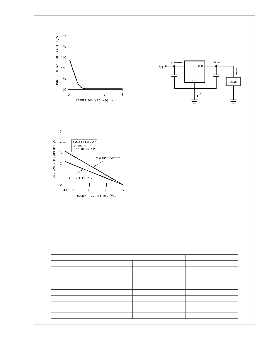
Figure 6 and Figure 7 show the information for the SOT-223
package. Figure 7 assumes a
(J-A)
of 74∞C/W for 1 ounce
copper and 51∞C/W for 2 ounce copper and a maximum
junction temperature of 125∞C.
00906307
D1 protects against C1
D2 protects against C2
FIGURE 3. Regulator with Protection Diodes
00906355
FIGURE 4.
(J-A)
vs Copper (1 ounce) Area for the
TO-263 Package
00906356
FIGURE 5. Maximum Power Dissipation vs T
AMB
for
the TO-263 Package
LM1
17/LM317A/LM317
www.national.com
7
Application Hints
(Continued)
The LM317 regulators have internal thermal shutdown to
protect the device from over-heating. Under all possible
operating conditions, the junction temperature of the LM317
must be within the range of 0∞C to 125∞C. A heatsink may be
required depending on the maximum power dissipation and
maximum ambient temperature of the application. To deter-
mine if a heatsink is needed, the power dissipated by the
regulator, P
D
, must be calculated:
I
IN
= I
L
+ I
G
P
D
= (V
IN
- V
OUT
) I
L
+ V
IN
I
G
Figure 8 shows the voltage and currents which are present in
the circuit.
The next parameter which must be calculated is the maxi-
mum allowable temperature rise, T
R
(max):
T
R
(max) = T
J
(max) - T
A
(max)
where T
J
(max) is the maximum allowable junction tempera-
ture (125∞C), and T
A
(max) is the maximum ambient tem-
perature which will be encountered in the application.
Using the calculated values for T
R
(max) and P
D
, the maxi-
mum allowable value for the junction-to-ambient thermal
resistance (
JA
) can be calculated:
JA
= T
R
(max)/P
D
If the maximum allowable value for
JA
is found to be
92∞C/W (Typical Rated Value) for TO-252 package, no
heatsink is needed since the package alone will dissipate
enough heat to satisfy these requirements. If the calculated
value for
JA
falls below these limits, a heatsink is required.
As a design aid, Table 1 shows the value of the
JA
of
TO-252 for different heatsink area. The copper patterns that
we used to measure these
JA
s are shown at the end of the
Application Notes Section. Figure 9 reflects the same test
results as what are in the Table 1
Figure 10 shows the maximum allowable power dissipation
vs. ambient temperature for the TO-252 device. Figure 11
shows the maximum allowable power dissipation vs. copper
area (in
2
) for the TO-252 device. Please see AN1028 for
power enhancement techniques to be used with SOT-223
and TO-252 packages.
TABLE 1.
JA
Different Heatsink Area
Layout
Copper Area
Thermal Resistance
Top Side (in
2
)*
Bottom Side (in
2
)
(
JA
∞C/W) TO-252
1
0.0123
0
103
2
0.066
0
87
3
0.3
0
60
4
0.53
0
54
5
0.76
0
52
6
1
0
47
7
0
0.2
84
8
0
0.4
70
9
0
0.6
63
00906357
FIGURE 6.
(J-A)
vs Copper (2 ounce) Area for the
SOT-223 Package
00906358
FIGURE 7. Maximum Power Dissipation vs T
AMB
for
the SOT-223 Package
00906360
FIGURE 8. Power Dissipation Diagram
LM1
17/LM317A/LM317
www.national.com
8
Application Hints
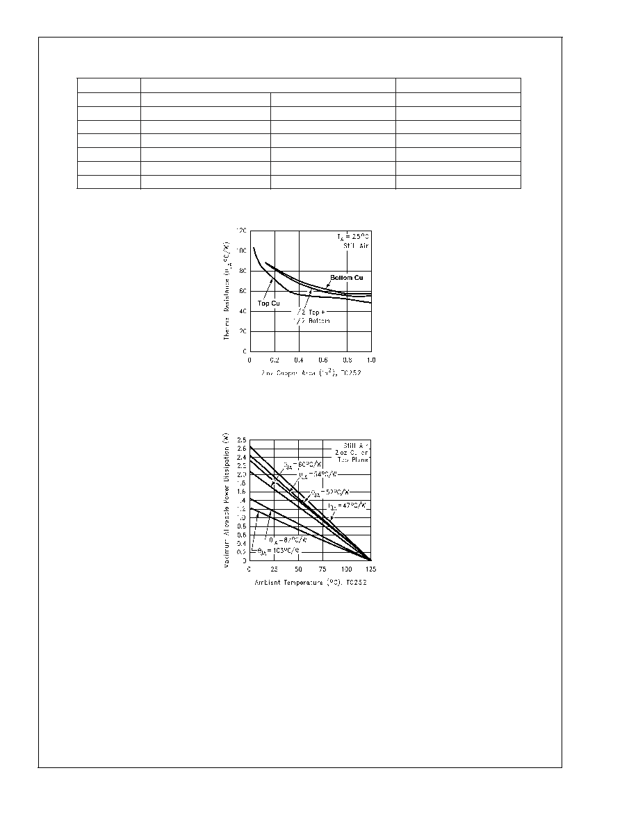
(Continued)
TABLE 1.
JA
Different Heatsink Area (Continued)
Layout
Copper Area
Thermal Resistance
10
0
0.8
57
11
0
1
57
12
0.066
0.066
89
13
0.175
0.175
72
14
0.284
0.284
61
15
0.392
0.392
55
16
0.5
0.5
53
Note: * Tab of device attached to topside of copper.
00906361
FIGURE 9.
JA
vs 2oz Copper Area for TO-252
00906363
FIGURE 10. Maximum Allowable Power Dissipation vs. Ambient Temperature for TO-252
LM1
17/LM317A/LM317
www.national.com
9
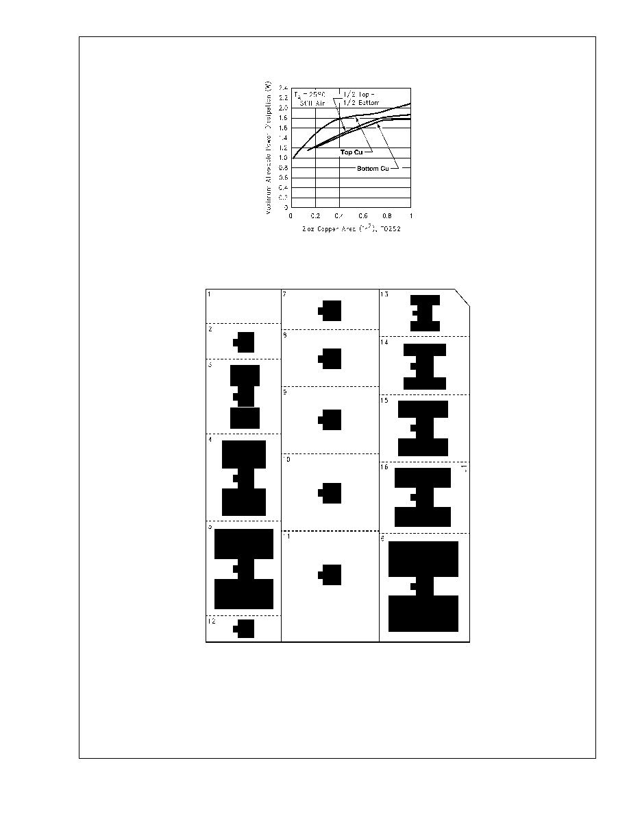
Application Hints
(Continued)
00906362
FIGURE 11. Maximum Allowable Power Dissipation vs. 2oz Copper Area for TO-252
00906364
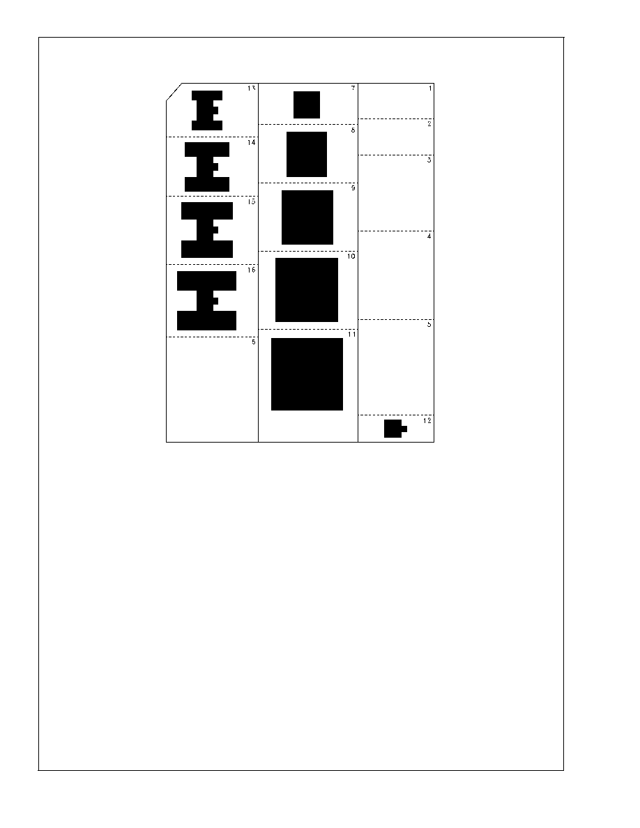
FIGURE 12. Top View of the Thermal Test Pattern in Actual Scale
LM1
17/LM317A/LM317
www.national.com
10
Application Hints
(Continued)
00906365
FIGURE 13. Bottom View of the Thermal Test Pattern in Actual Scale
LM1
17/LM317A/LM317
www.national.com
11
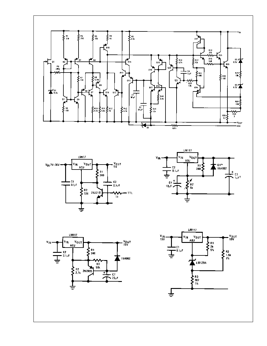
Schematic Diagram
00906308
Typical Applications
5V Logic Regulator with Electronic Shutdown
*
00906303
*Min. output ) 1.2V
Slow Turn-On 15V Regulator
00906309
Adjustable Regulator with Improved Ripple Rejection
00906310
Solid tantalum
*Discharges C1 if output is shorted to ground
High Stability 10V Regulator
00906311
LM1
17/LM317A/LM317
www.national.com
12

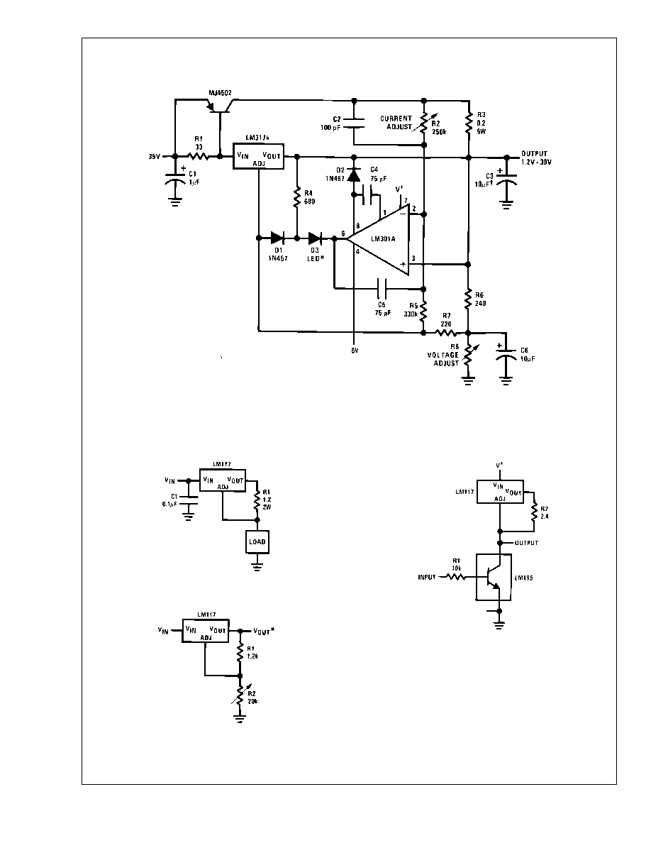
Typical Applications
(Continued)
High Current Adjustable Regulator
00906312
Optional -- improves ripple rejection
Solid tantalum
*Minimum load current = 30 mA
0 to 30V Regulator
00906313
Full output current not available at high input-output voltages
Power Follower
00906314
LM1
17/LM317A/LM317
www.national.com
13
Typical Applications
(Continued)
5A Constant Voltage/Constant Current Regulator
00906315
Solid tantalum
*Lights in constant current mode
1A Current Regulator
00906316
1.2V≠20V Regulator with Minimum Program Current
00906317
*Minimum load current ) 4 mA
High Gain Amplifier
00906318
LM1
17/LM317A/LM317
www.national.com
14
Typical Applications
(Continued)
Low Cost 3A Switching Regulator
00906319
Solid tantalum
*Core -- Arnold A-254168-2 60 turns
4A Switching Regulator with Overload Protection
00906320
Solid tantalum
*Core -- Arnold A-254168-2 60 turns
Precision Current Limiter
00906321
LM1
17/LM317A/LM317
www.national.com
15
Typical Applications
(Continued)
Tracking Preregulator
00906322
Current Limited Voltage Regulator
00906323
(Compared to LM117's higher current limit)
-- At 50 mA output only
3
/
4
volt of drop occurs in R
3
and R
4
Adjusting Multiple On-Card Regulators with Single Control
*
00906324
*All outputs within
±
100 mV
Minimum load -- 10 mA
LM1
17/LM317A/LM317
www.national.com
16
Typical Applications
(Continued)
AC Voltage Regulator
00906325
12V Battery Charger
00906326
Use of R
S
allows low charging rates with fully charged battery.
50 mA Constant Current Battery Charger
00906327
LM1
17/LM317A/LM317
www.national.com
17
Typical Applications
(Continued)
Adjustable 4A Regulator
00906328
Current Limited 6V Charger
00906329
*Sets peak current (0.6A for 1
)
**The 1000 µF is recommended to filter out input transients
Digitally Selected Outputs
00906302
*Sets maximum V
OUT
LM1
17/LM317A/LM317
www.national.com
18
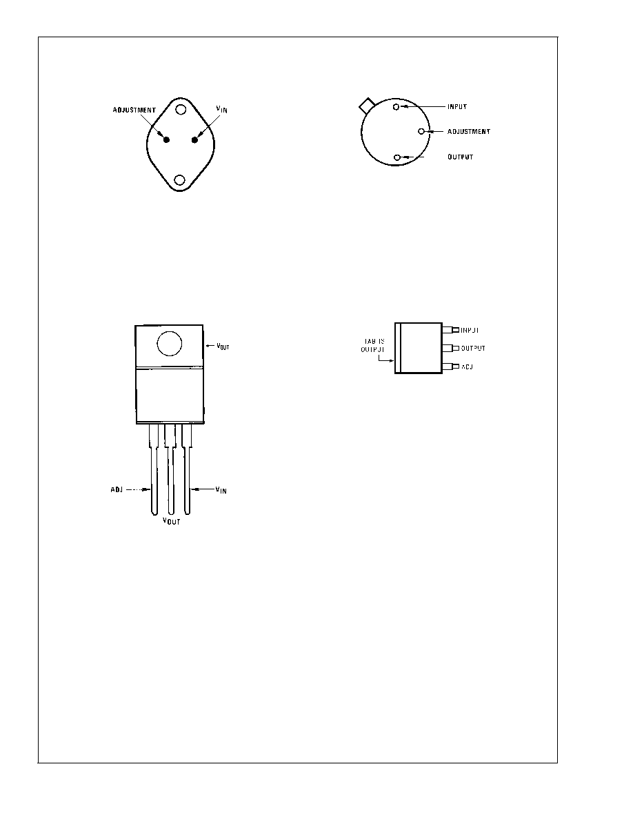
Connection Diagrams
(TO-3)
Metal Can Package
(TO-39)
Metal Can Package
00906330
CASE IS OUTPUT
Bottom View
Steel Package
Order Number LM117K STEEL
or LM317K STEEL
See NS Package Number K02A
Order Number LM117K/883
See NS Package Number K02C
00906331
CASE IS OUTPUT
Bottom View
Order Number LM117H, LM117H/883,
LM317AH or LM317H
See NS Package Number H03A
(TO-220)
Plastic Package
(TO-263) Surface-Mount Package
00906332
Front View
Order Number LM317AT or LM317T
See NS Package Number T03B
00906335
Top View
LM1
17/LM317A/LM317
www.national.com
19
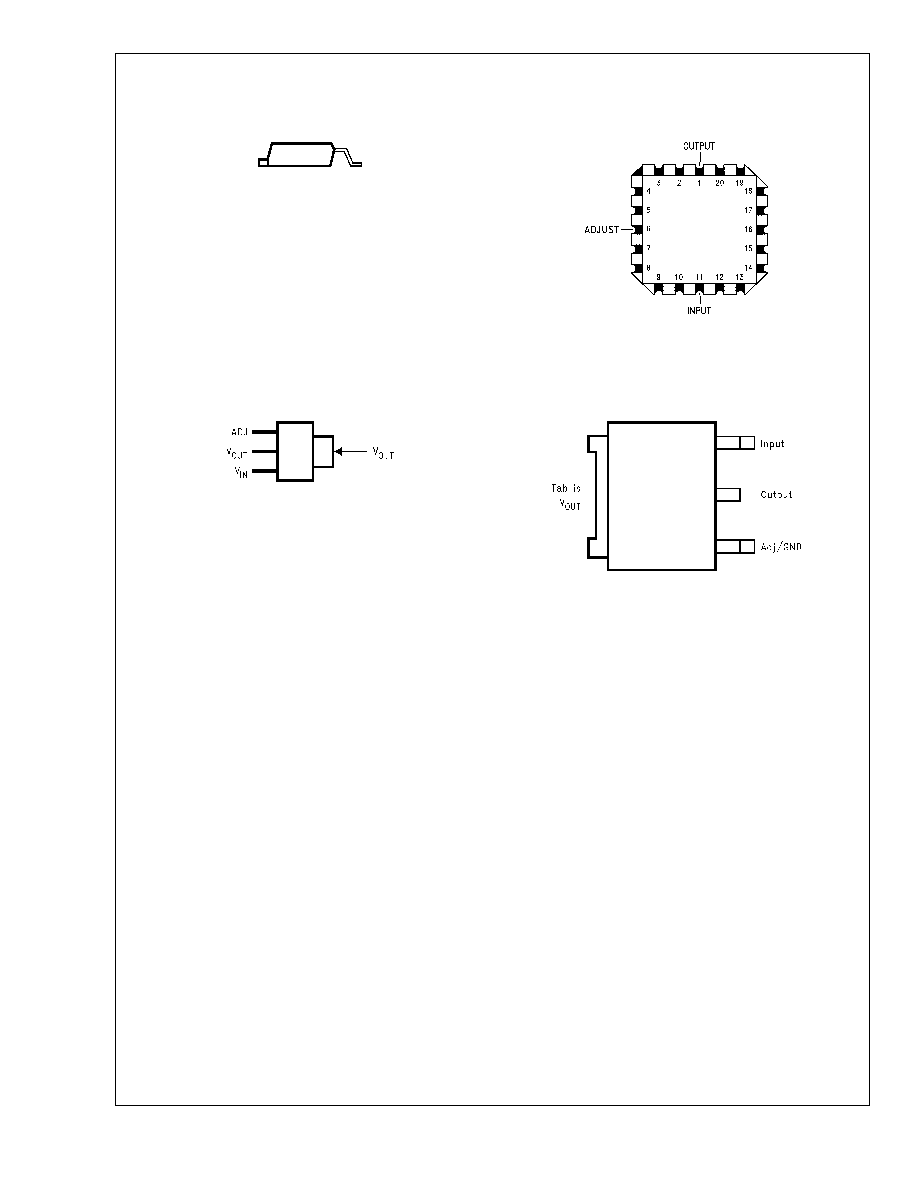
Connection Diagrams
(Continued)
Ceramic Leadless
Chip Carrier
00906336
Side View
Order Number LM317S
See NS Package Number TS3B
00906334
Top View
Order Number LM117E/883
See NS Package Number E20A
4-Lead SOT-223
TO-252 (D-Pak)
00906359
Front View
Order Part Number LM317EMP or LM317AEMP
See NSC Package Number MA04A
00906366
Front View
Order Part Number LM317MDT
See NSC Package Number TD03B
LM1
17/LM317A/LM317
www.national.com
20
Physical Dimensions
inches (millimeters)
unless otherwise noted
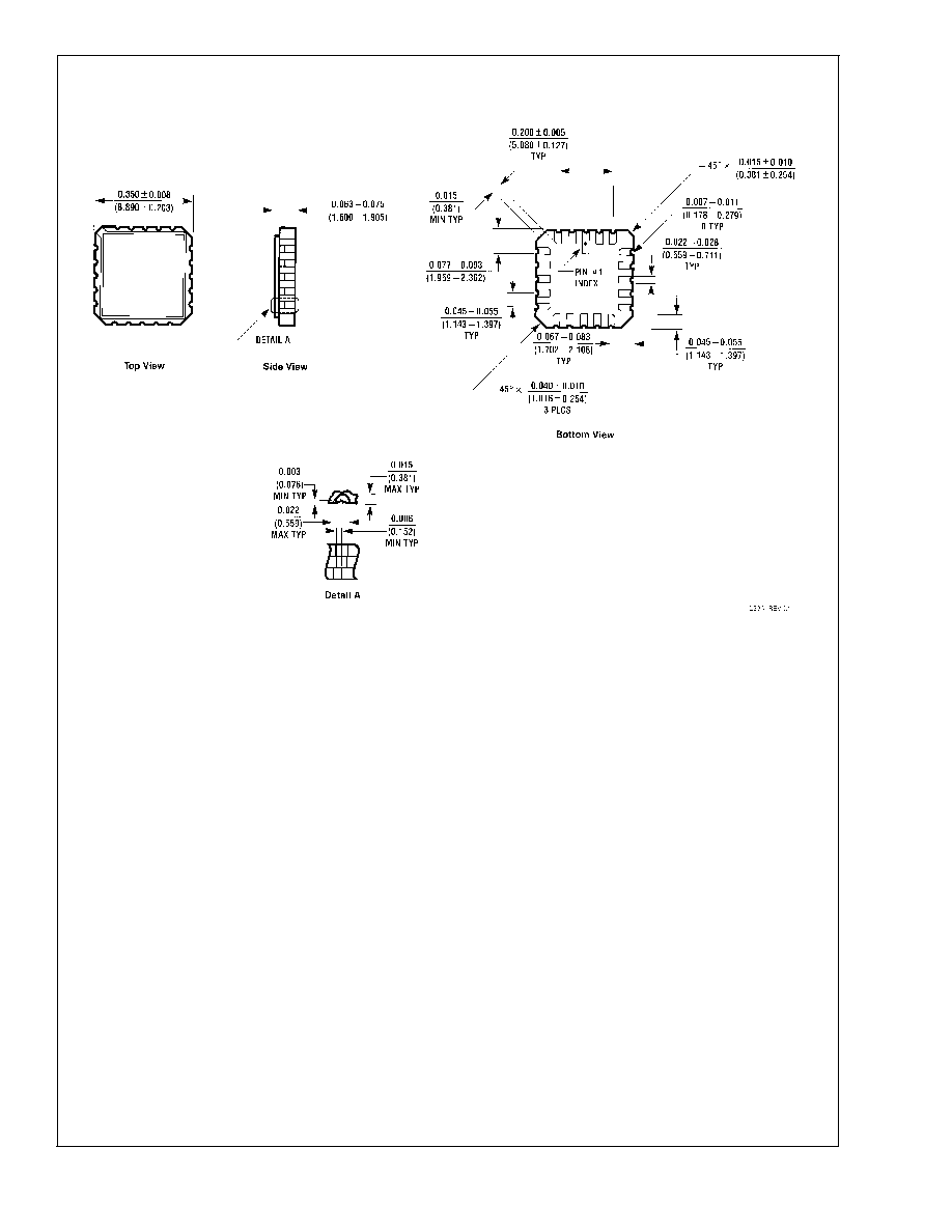
Ceramic Leadless Chip Carrier
Order Number LM117E/883
NS Package Number E20A
LM1
17/LM317A/LM317
www.national.com
21
Physical Dimensions
inches (millimeters) unless otherwise noted (Continued)
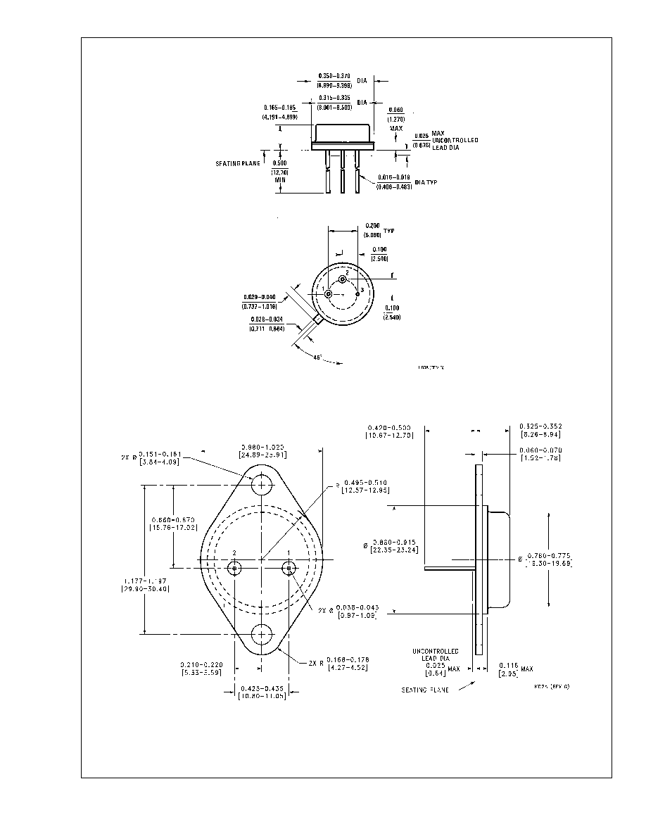
(TO-39) Metal Can Package
Order Number LM117H, LM117H/883, LM317AH or LM317H
NS Package Number H03A
TO-3 Metal Can Package (K)
Order Number LM117K STEEL,
LM117K STEEL/883, or LM317K STEEL
NS Package Number K02A
LM1
17/LM317A/LM317
www.national.com
22
Physical Dimensions
inches (millimeters) unless otherwise noted (Continued)
TO-3 Metal Can Package (K)
Mil-Aero Product
Order Number LM117K/883
NS Package Number K02C
LM1
17/LM317A/LM317
www.national.com
23
Physical Dimensions
inches (millimeters) unless otherwise noted (Continued)
4-Lead SOT-223 Package
Order Number LM317AEMP or LM317EMP
NS Package Number MP04A
(TO-220) Outline Drawing
Order Number LM317AT or LM317T
NS Package Number T03B
LM1
17/LM317A/LM317
www.national.com
24
Physical Dimensions
inches (millimeters) unless otherwise noted (Continued)
Order Number LM317S
NS Package Number TS3B
Order Number LM317MDT
NS Package Number TD03B
LM1
17/LM317A/LM317
www.national.com
25
Notes
LIFE SUPPORT POLICY
NATIONAL'S PRODUCTS ARE NOT AUTHORIZED FOR USE AS CRITICAL COMPONENTS IN LIFE SUPPORT
DEVICES OR SYSTEMS WITHOUT THE EXPRESS WRITTEN APPROVAL OF THE PRESIDENT AND GENERAL
COUNSEL OF NATIONAL SEMICONDUCTOR CORPORATION. As used herein:
1. Life support devices or systems are devices or
systems which, (a) are intended for surgical implant
into the body, or (b) support or sustain life, and
whose failure to perform when properly used in
accordance with instructions for use provided in the
labeling, can be reasonably expected to result in a
significant injury to the user.
2. A critical component is any component of a life
support device or system whose failure to perform
can be reasonably expected to cause the failure of
the life support device or system, or to affect its
safety or effectiveness.
National Semiconductor
Corporation
Americas
Email: support@nsc.com
National Semiconductor
Europe
Fax: +49 (0) 180-530 85 86
Email: europe.support@nsc.com
Deutsch Tel: +49 (0) 69 9508 6208
English
Tel: +44 (0) 870 24 0 2171
FranÁais Tel: +33 (0) 1 41 91 8790
National Semiconductor
Asia Pacific Customer
Response Group
Tel: 65-2544466
Fax: 65-2504466
Email: ap.support@nsc.com
National Semiconductor
Japan Ltd.
Tel: 81-3-5639-7560
Fax: 81-3-5639-7507
www.national.com
LM1
17/LM317A/LM317
3-T
erminal
Adjustable
Regulator
National does not assume any responsibility for use of any circuitry described, no circuit patent licenses are implied and National reserves the right at any time without notice to change said circuitry and specifications.