LM317L
3-Terminal Adjustable Regulator
General Description
The LM317L is an adjustable 3-terminal positive voltage
regulator capable of supplying 100mA over a 1.2V to 37V
output range. It is exceptionally easy to use and requires
only two external resistors to set the output voltage. Further,
both line and load regulation are better than standard fixed
regulators. Also, the LM317L is available packaged in a
standard TO-92 transistor package which is easy to use.
In addition to higher performance than fixed regulators, the
LM317L offers full overload protection. Included on the chip
are current limit, thermal overload protection and safe area
protection. All overload protection circuitry remains fully func-
tional even if the adjustment terminal is disconnected.
Normally, no capacitors are needed unless the device is
situated more than 6 inches from the input filter capacitors in
which case an input bypass is needed. An optional output
capacitor can be added to improve transient response. The
adjustment terminal can be bypassed to achieve very high
ripple rejection ratios which are difficult to achieve with stan-
dard 3-terminal regulators.
Besides replacing fixed regulators, the LM317L is useful in a
wide variety of other applications. Since the regulator is
"floating" and sees only the input-to-output differential volt-
age, supplies of several hundred volts can be regulated as
long as the maximum input-to-output differential is not ex-
ceeded.
Also, it makes an especially simple adjustable switching
regulator, a programmable output regulator, or by connecting
a fixed resistor between the adjustment and output, the
LM317L can be used as a precision current regulator. Sup-
plies with electronic shutdown can be achieved by clamping
the adjustment terminal to ground which programs the out-
put to 1.2V where most loads draw little current.
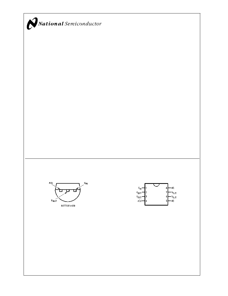
The LM317L is available in a standard TO-92 transistor
package, the SO-8 package, and 6-Bump micro SMD pack-
age. The LM317L is rated for operation over a -25∞C to
125∞C range.
Features
n
Adjustable output down to 1.2V
n
Guaranteed 100 mA output current
n
Line regulation typically 0.01%V
n
Load regulation typically 0.1%
n
Current limit constant with temperature
n
Eliminates the need to stock many voltages
n
Standard 3-lead transistor package
n
80 dB ripple rejection
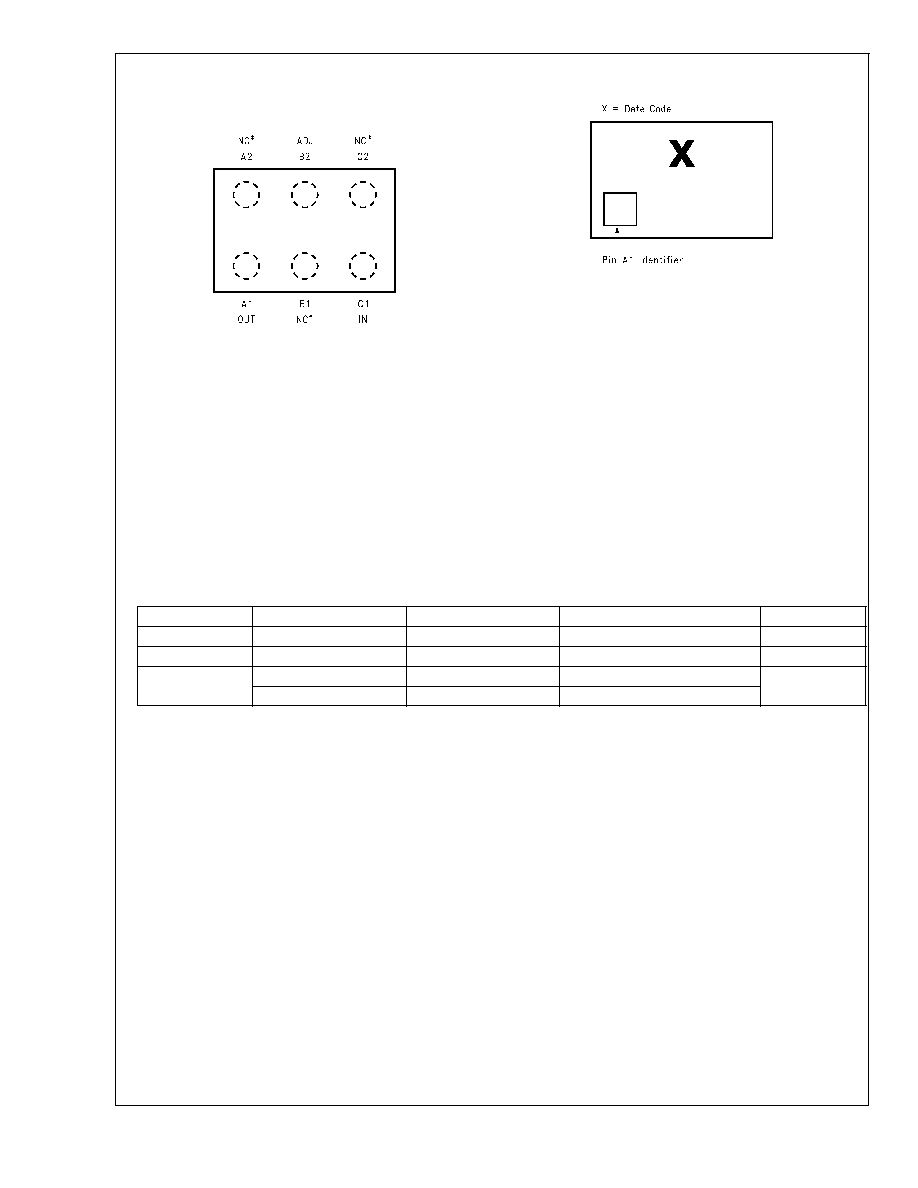
n
Available in TO-92, SO-8, or 6-Bump micro SMD
package
n
Output is short circuit protected
n
See AN-1112 for micro SMD considerations
Connection Diagrams
TO-92 Plastic package
DS009064-4
8-Pin SOIC
DS009064-5
Top View
March 2002
LM317L
3-T
erminal
Adjustable
Regulator
© 2002 National Semiconductor Corporation
DS009064
www.national.com

Absolute Maximum Ratings
(Note 1)
If Military/Aerospace specified devices are required,
please contact the National Semiconductor Sales Office/
Distributors for availability and specifications.
Power Dissipation
Internally Limited
Input-Output Voltage Differential
40V
Operating Junction Temperature
Range
-40∞C to +125∞C
Storage Temperature
-55∞C to +150∞C
Lead Temperature
(Soldering, 4 seconds)
260∞C
Output is Short Circuit Protected
ESD rating to be determined.
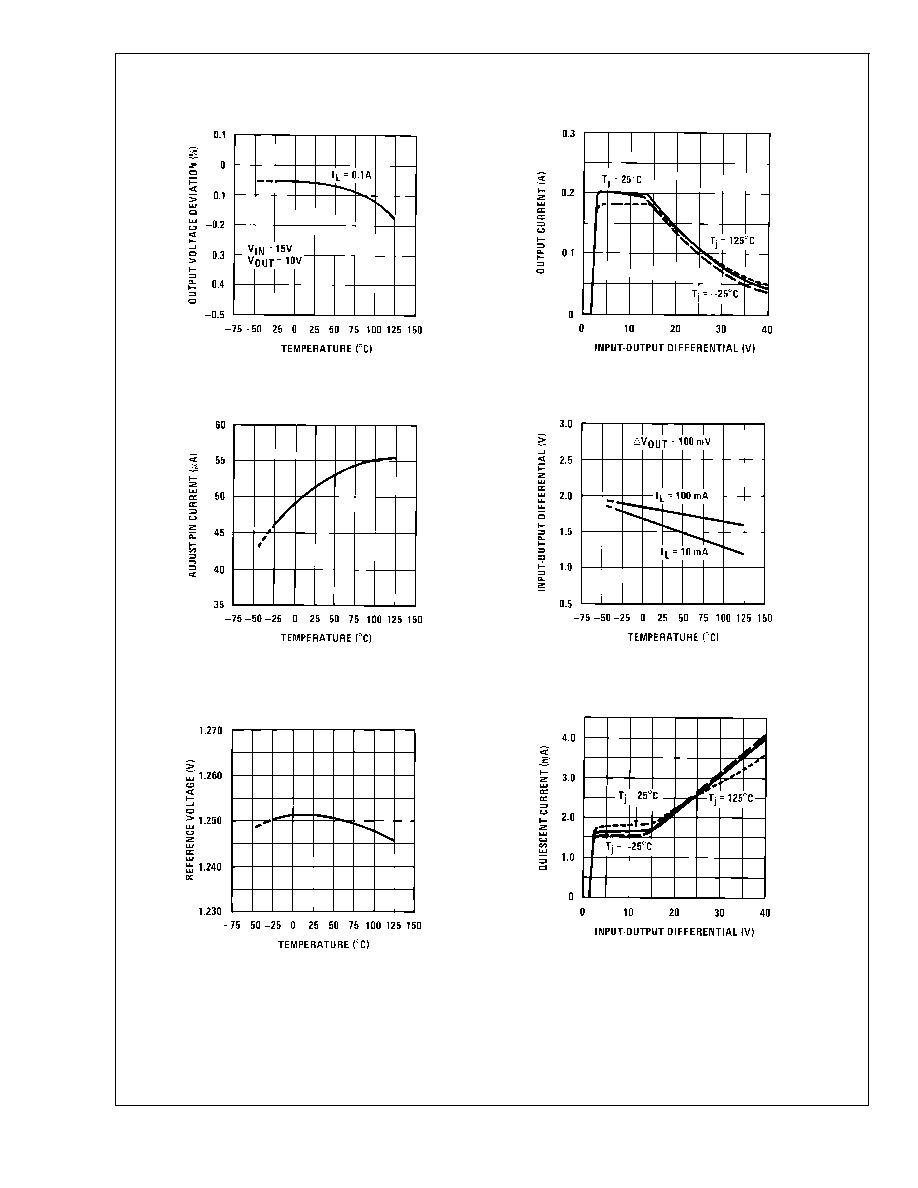
Electrical Characteristics
(Note 2)
Parameter
Conditions
Min
Typ
Max
Units
Line Regulation
T
J
= 25∞C, 3V
(V
IN
- V
OUT
)
40V, I
L
20mA (Note 3)
0.01
0.04
%/V
Load Regulation
T
J
= 25∞C, 5mA
I
OUT
I
MAX
, (Note 3)
0.1
0.5
%
Thermal Regulation
T
J
= 25∞C, 10ms Pulse
0.04
0.2
%/W
Adjustment Pin Current
50
100
µA
Adjustment Pin Current
5mA
I
L
100mA
0.2
5
µA
Change
3V
(V
IN
- V
OUT
)
40V, P
625mW
Reference Voltage
3V
(V
IN
- V
OUT
)
40V, (Note 4)
1.20
1.25
1.30
V
5mA
I
OUT
100mA, P
625mW
Line Regulation
3V
(V
IN
- V
OUT
)
40V, I
L
20mA (Note 3)
0.02
0.07
%/V
Load Regulation
5mA
I
OUT
100mA, (Note 3)
0.3
1.5
%
Temperature Stability
T
MIN
T
J
T
Max
0.65
%
Minimum Load Current
(V
IN
- V
OUT
)
40V
3.5
5
mA
3V
(V
IN
- V
OUT
)
15V
1.5
2.5
Current Limit
3V
(V
IN
- V
OUT
)
13V
100
200
300
mA
(V
IN
- V
OUT
) = 40V
25
50
150
mA
Rms Output Noise, % of V
OUT
T
J
= 25∞C, 10Hz
f
10kHz
0.003
%
Ripple Rejection Ratio
V
OUT
= 10V, f = 120Hz, C
ADJ
= 0
65
dB
C
ADJ
= 10µF
66
80
dB
Long-Term Stability
T
J
= 125∞C, 1000 Hours
0.3
1
%
Thermal Resistance
Z Package 0.4" Leads
180
∞C/W
Junction to Ambient
Z Package 0.125 Leads
160
∞C/W
SO-8 Package
165
∞C/W
6-Bump micro SMD
290
∞C/W
Thermal Rating of SO
Package
165
∞C/W
Note 1: "Absolute Maximum Ratings" indicate limits beyond which damage to the device may occur. Operating Ratings indicate conditions for which the device is
functional, but do not guarantee specific performance limits.
Note 2: Unless otherwise noted, these specifications apply: -25∞C
T
j
125∞C for the LM317L; V
IN
- V
OUT
= 5V and I
OUT
= 40 mA. Although power dissipation
is internally limited, these specifications are applicable for power dissipations up to 625 mW. I
MAX
is 100 mA.
Note 3: Regulation is measured at constant junction temperature, using pulse testing with a low duty cycle. Changes in output voltage due to heating effects are
covered under the specification for thermal regulation.
Note 4: Thermal resistance of the TO-92 package is 180∞C/W junction to ambient with 0.4" leads from a PC board and 160∞C/W junction to ambient with 0.125" lead
length to PC board.
LM317L
www.national.com
3