 | –≠–ª–µ–∫—Ç—Ä–æ–Ω–Ω—ã–π –∫–æ–º–ø–æ–Ω–µ–Ω—Ç: LM3204 | –°–∫–∞—á–∞—Ç—å:  PDF PDF  ZIP ZIP |
LM3204
Miniature, Adjustable, Step-Down DC-DC Converter with
Bypass Mode for RF Power Amplifiers
General Description
The LM3204 is a DC-DC converter optimized for powering
RF power amplifiers (PAs) from a single Lithium-Ion cell. It
steps down an input voltage of 2.7V to 5.5V to an adjustable
output voltage of 0.8V to 3.6V. The output voltage is set
using an analog input ( V
CON
) for optimizing efficiency of the
RF PA at various power levels.
The LM3204 offers superior features and performance for
mobile phones and similar RF PA applications. Fixed-
frequency PWM mode minimizes RF interference. Bypass
mode turns on an internal bypass switch to power the PA
directly from the battery. LM3204 has both forced and auto-
matic bypass modes. Shutdown mode turns the device off
and reduces battery consumption to 0.1µA (typ.).
The LM3204 is available in a 10-pin lead free micro SMD
package. A high switching frequency (2MHz) allows use of
tiny surface-mount components. Only three small external
surface-mount components, an inductor and two ceramic
capacitors are required.
Features
n
2MHz (typ.) PWM Switching Frequency
n
Operates from a single Li-Ion cell (2.7V to 5.5V)
n
Adjustable Output Voltage (0.8V to 3.6V)
n
Fast Turn on time when Enabled (50µs Typ.), 3GPP
Compliant
n
300mA Maximum load capability (PWM mode)
n
500mA Maximum load capability (Bypass mode)
n
PWM, Forced and Automatic Bypass Mode
n
High Efficiency (96% Typ. at 3.6V
IN
, 3.2V
OUT
at 120mA)
n
10-pin micro SMD Package
n
Current Overload Protection
n
Thermal Overload Protection
Applications
n
Cellular Phones
n
Hand-Held Radios
n
RF PC Cards
n
Battery Powered RF Devices
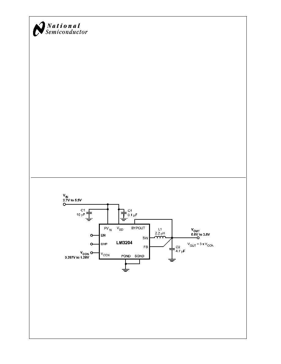
Typical Application
20138901
November 2005
LM3204
Miniature,
Adjustable,
Step-Down
DC-DC
Converter
with
Bypass
Mode
for
RF
Power
Amplifiers
© 2005 National Semiconductor Corporation
DS201389
www.national.com
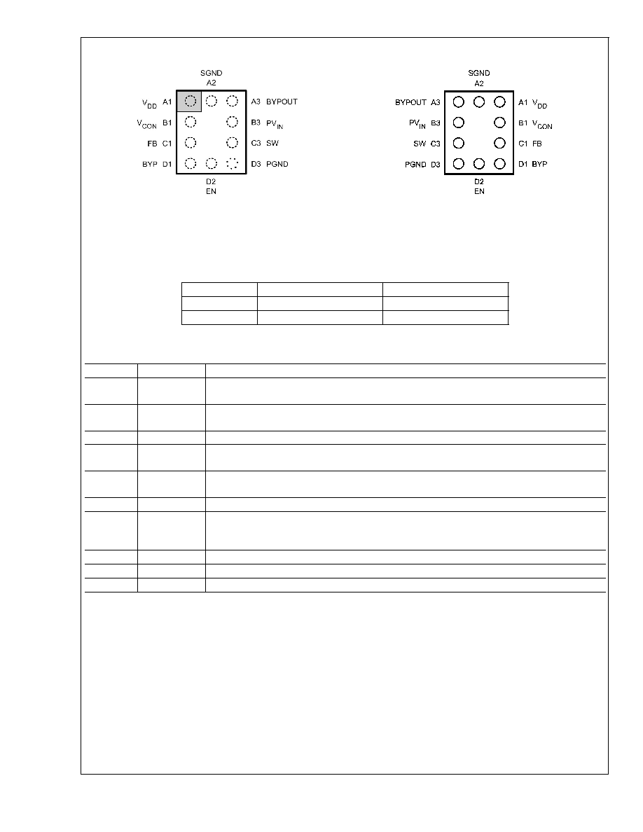
Connection Diagrams
20138902
Top View
20138903
Bottom View
10≠Bump Thin Micro SMD Package, Large Bump
See NS Package Number TLP10NHA
Order Information
Order Number
Package Marking (Note)
Supplied As
LM3204TL
XYTT SJDB
250 Units, Tape and Reel
LM3204TLX
XYTT SJDB
3000 Units, Tape and Reel
Note: The package marking "XY" designates the date code. "TT" is a NSC internal code for die traceability.
Pin Description
Pin #
Name
Description
A1
V
DD
Analog Supply Input. A 0.1µF ceramic capacitor is recommended to be placed as close to this pin
as possible. (Figure 1)
B1
V
CON
Voltage Control Analog input. V
CON
controls V
OUT
in PWM mode. Set: V
OUT
= 3 x V
CON.
Do not
leave floating.
C1
FB
Feedback Analog Input. Connect to the output at the output filter capacitor. (Figure 1)
D1
BYP
Bypass. Use this digital input to command operation in Bypass mode. Set BYP low (
<
0.4V) for
normal operation.
D2
EN
Enable Input. Set this digital input high (
>
1.2V) after Vin
>
2.7V for normal operation. For
shutdown, set low (
<
0.4V).
D3
PGND
Power Ground
C3
SW
Switching Node connection to the internal PFET switch and NFET synchronous rectifier.
Connect to an inductor with a saturation current rating that exceeds the maximum Switch Peak
Current Limit specification of the LM3204.
B3
PV
IN
Power Supply Voltage Input to the internal PFET switch and Bypass FET. (Figure 1)
A3
BYPOUT
Bypass FET Drain. Connect to the output capacitor. (Figure 1) Do not leave floating.
A2
SGND
Analog and Control Ground
LM3204
www.national.com
2
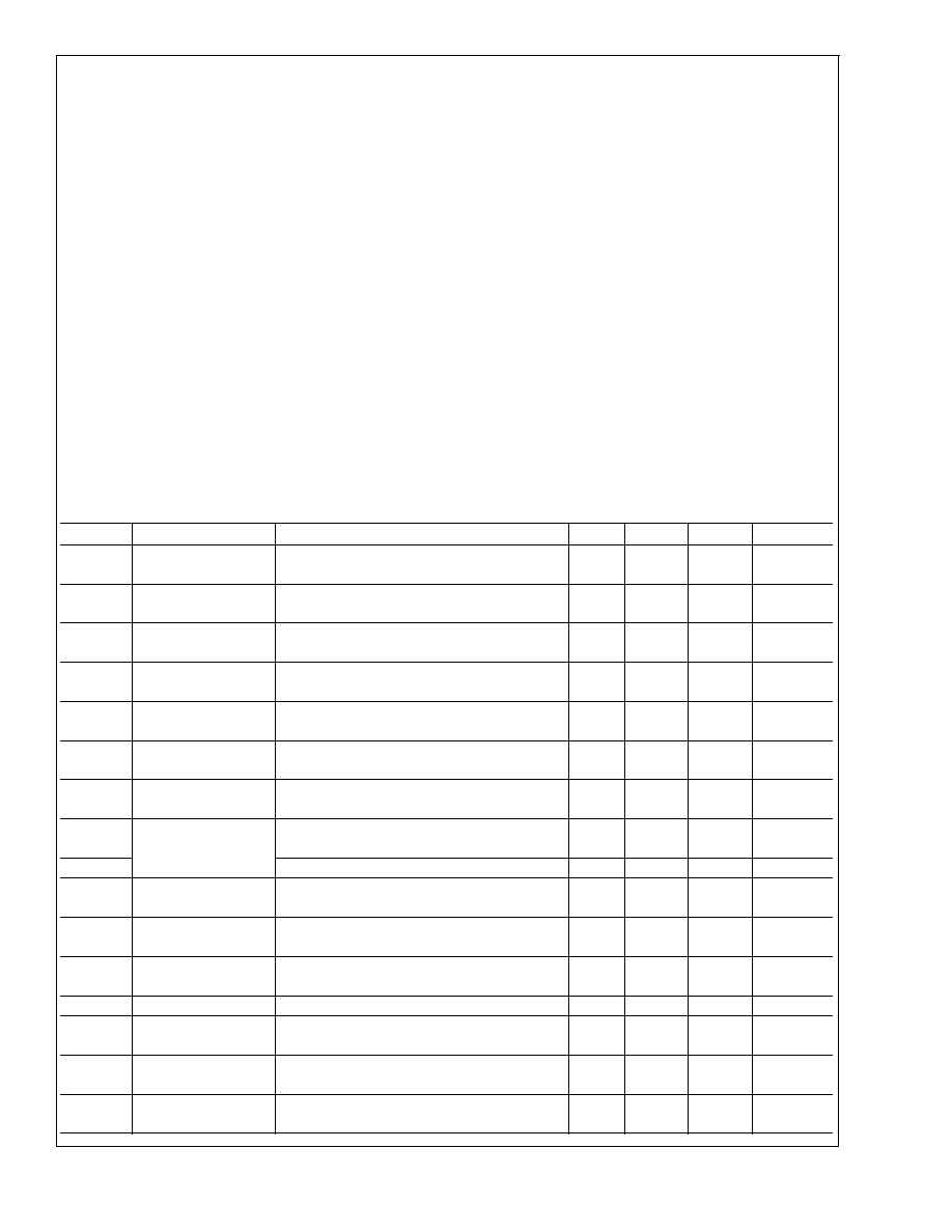
Absolute Maximum Ratings
(Notes 1, 2)
If Military/Aerospace specified devices are required,
please contact the National Semiconductor Sales Office/
Distributors for availability and specifications.
V
DD
, PV
IN
to SGND
-0.2V to +6.0V
PGND to SGND
-0.2V to +0.2V
EN, FB, BYP, V
CON
(SGND -0.2V)
to (V
DD
+0.2V)
w/6.0V max
SW, BYPOUT
(PGND -0.2V)
to (PV
IN
+0.2V)
w/6.0V max
PV
IN
to V
DD
-0.2V to +0.2V
Continuous Power Dissipation
(Note 3)
Internally Limited
Junction Temperature (T
J-MAX
)
+150∞C
Storage Temperature Range
-65∞C to +150∞C
Maximum Lead Temperature
(Soldering, 10 sec.)
+260∞C
ESD Rating (Note 4)
Human Body Model
Machine Model
2.0kV
200V
Operating Ratings
(Notes 1, 2)
Input Voltage Range
2.7V to 5.5V
Recommended Load Current
PWM Mode
0mA to 300mA
Bypass Mode
0mA to 500mA
Junction Temperature (T
J
) Range
-30∞C to +125∞C
Ambient Temperature (T
A
) Range
(Note 5)
-30∞C to +85∞C
Thermal Properties
Junction-to-Ambient Thermal
100∞C/W
Resistance (
JA
), TLP10 Package (Note 6)
Electrical Characteristics
(Notes 2, 7) Limits in standard typeface are for T
A
= T
J
= 25∞C. Limits in bold-
face type apply over the full operating ambient temperature range (-30∞C
T
A
= T
J
+85∞C). Unless otherwise noted, speci-
fications apply to the LM3204 with: PV
IN
= V
DD
= EN = 3.6V, BYP = 0V.
Symbol
Parameter
Conditions
Min
Typ
Max
Units
V
IN
Input Voltage Range
(Note 8)
PV
IN
= V
DD
= V
IN
2.7
5.5
V
V
FB, MIN
Feedback Voltage at
Minimum Setting
V
CON
= 0.267V, V
IN
= 3.6V
0.75
0.800
0.85
V
V
FB, MAX
Feedback Voltage at
Maximum Setting
V
CON
= 1.20V, V
IN
= 4.2V
3.528
3.600
3.672
V
OVP
Over-Voltage
Protection Threshold
(Note 9)
330
400
mV
V
BYPASS-
Auto Bypass Detection
Negative Threshold
(Note 10)
160
250
320
mV
V
BYPASS+
Auto Bypass Detection
Positive Threshold
(Note 10)
350
450
540
mV
I
SHDN
Shutdown Supply
Current (Note 11)
EN = SW = BYPOUT = V
CON
= FB = 0V
0.1
3
µA
I
Q_PWM
DC Bias Current into
V
DD
V
CON
= 0.267V, FB = 2V, BYPOUT = 0V,
No-Load
720
800
µA
I
Q_BYP
BYP = 3.6V, V
CON
= 0.5V, No-Load
720
800
µA
R
DSON (P)
Pin-Pin Resistance for
PFET
I
SW
= 500mA
320
450
m
R
DSON (N)
Pin-Pin Resistance for
N-FET
I
SW
= - 200mA
310
450
m
R
DSON
(BYP)
Pin-Pin Resistance for
Bypass FET
I
BYPOUT
= 500mA
85
120
m
I
LIM-PFET
Switch Current Limit
(Note 12)
700
820
940
mA
I
LIM-BYP
Bypass FET Current
Limit
(Note 13)
800
1000
1200
mA
F
OSC
Internal Oscillator
Frequency
1.7
2
2.2
MHz
V
IH
Logic High Input
Threshold for EN, BYP
1.20
V
LM3204
www.national.com
3
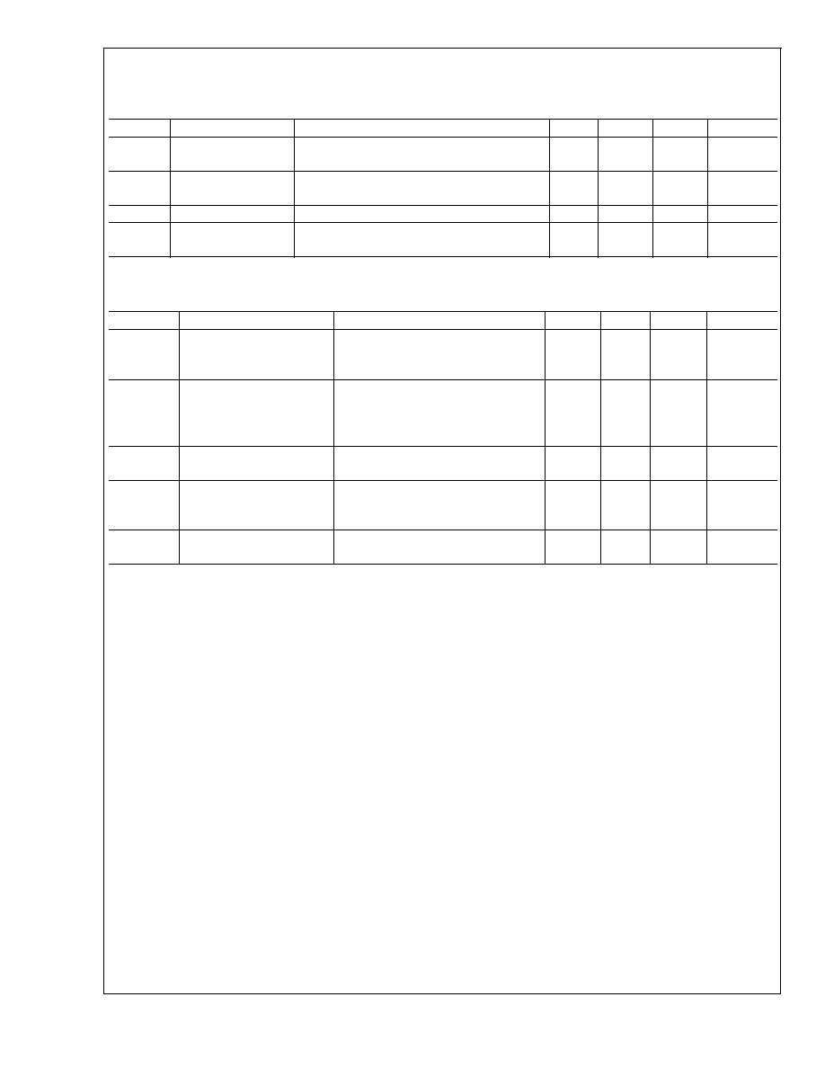
Electrical Characteristics
(Notes 2, 7) Limits in standard typeface are for T
A
= T
J
= 25∞C. Limits in boldface
type apply over the full operating ambient temperature range (-30∞C
T
A
= T
J
+85∞C). Unless otherwise noted,
specifications apply to the LM3204 with: PV
IN
= V
DD
= EN = 3.6V, BYP = 0V. (Continued)
Symbol
Parameter
Conditions
Min
Typ
Max
Units
V
IL
Logic Low Input
Threshold for EN, BYP
0.4
V
I
PIN
Pin Pull Down Current
for EN, BYP
EN, BYP = 3.6V
5
10
µA
Gain
V
CON
to V
OUT
Gain
3
V/V
I
CON
V
CON
Input Leakage
Current
V
CON
= 1.2V
10
nA
System Characteristics
The following spec table entries are guaranteed by design if the component values
in the typical application circuit are used. These parameters are not guaranteed by production testing.
Symbol
Parameter
Conditions
Min
Typ
Max
Units
T
RESPONSE
Time for V
OUT
to Rise from
0.8V to 3.4V in PWM Mode
V
IN
= 4.2V, C
OUT
= 4.7µF,
R
LOAD
= 15
L = 2.2 µH (I
SAT
>
0.94A)
25
µs
T
STARTUP
Time for V
OUT
to rise to 3.4V
in PWM Mode
(Note 14)
V
IN
= 4.2V, C
OUT
= 4.7µF,
R
LOAD
= 15
L = 2.2µH (I
SAT
= 0.94A)
EN = Low to High
50
µs
C
CON
V
CON
Input Capacitance
V
CON
= 1V,
Test frequency = 100kHz
15
pF
T
ON_BYP
Bypass FET Turn On Time
In Bypass Mode
V
IN
= 3.6V, V
CON
= 0.267V,
C
OUT
= 4.7µF, R
LOAD
= 15
BYP = Low to High
30
µs
T
BYP
Auto Bypass Detect Delay
Time
(Note 10)
10
15
20
µs
Note 1: Absolute Maximum Ratings indicate limits beyond which damage to the component may occur. Operating Ratings are conditions under which operation of
the device is guaranteed. Operating Ratings do not imply guaranteed performance limits. For guaranteed performance limits and associated test conditions, see the
Electrical Characteristics tables.
Note 2: All voltages are with respect to the potential at the GND pins.
Note 3: Internal thermal shutdown circuitry protects the device from permanent damage. Thermal shutdown engages at T
J
= 150∞C (typ.) and disengages at T
J
=
130∞C (typ.).
Note 4: The Human body model is a 100pF capacitor discharged through a 1.5k
resistor into each pin. (MIL-STD-883 3015.7) The machine model is a 200pF
capacitor discharged directly into each pin. National Semiconductor recommends that all integrated circuits be handled with appropriate precautions. Failure to
observe proper ESD handling techniques can result in damage.
Note 5: In applications where high power dissipation and/or poor package thermal resistance is present, the maximum ambient temperature may have to be
de-rated. Maximum ambient temperature (T
A-MAX
) is dependent on the maximum operating junction temperature (T
J-MAX-OP
= 125∞C), the maximum power
dissipation of the device in the application (P
D-MAX
), and the junction-to ambient thermal resistance of the part/package in the application (
JA
), as given by the
following equation: T
A-MAX
= T
J-MAX-OP
≠ (
JA
x P
D-MAX
).
Note 6: Junction-to-ambient thermal resistance (
JA
) is taken from thermal measurements, performed under the conditions and guidelines set forth in the JEDEC
standard JESD51-7. A 1" x 1", 4 layer, 1.5oz. Cu board was used for the measurements.
Note 7: Min and Max limits are guaranteed by design, test, or statistical analysis. Typical numbers are not guaranteed, but do represent the most likely norm.
Note 8: The LM3204 is designed for mobile phone applications where turn-on after power-up is controlled by the system controller and where requirements for a
small package size overrule increased die size for internal Under Voltage Lock-Out (UVLO) circuitry. Thus, it should be kept in shutdown by holding the EN pin low
until the input voltage exceeds 2.7V.
Note 9: Over-Voltage protection (OVP) threshold is the voltage above the nominal V
OUT
where the OVP comparator turns off the PFET switch while in PWM mode.
Note 10: V
IN
is compared to the programmed output voltage (V
OUT
). When V
IN
≠V
OUT
falls below V
BYPASS-
for longer than T
BYP
the Bypass FET turns on and the
switching FETs turn off. This is called the Bypass mode. The device comes out of Bypass mode when V
IN
≠V
OUT
exceeds V
BYPASS
+
for longer than T
BYP
, and PWM
mode returns. The hysteresis for the bypass detection threshold V
BYPASS
+
≠ V
BYPASS
- will always be positive and will be approximately 200mV (typ.).
Note 11: Shutdown current includes leakage current of PFET and Bypass FET.
Note 12: Electrical Characteristic table reflects open loop data (FB=0V and current drawn from SW pin ramped up until cycle by cycle current limit is activated).
Refer to datasheet curves for closed loop data and its variation with regards to supply voltage and temperature. Closed loop current limit is the peak inductor current
measured in the application circuit by increasing output current until output voltage drops by 10%.
Note 13: Bypass FET current limit is defined as the load current at which the FB voltage is 1V lower than V
IN
.
Note 14: The startup time is the time to reach 90% of 3.4V nominal output voltage from the EN being low to high.
LM3204
www.national.com
4
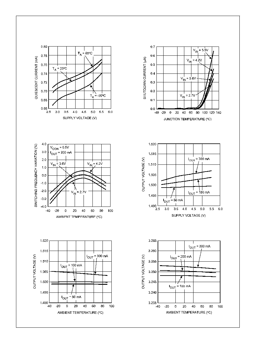
Typical Performance Characteristics
(Circuit in Figure 1, PV
IN
= V
DD
= EN = 3.6V, BYP = 0V, T
A
=
25∞C, unless otherwise noted)
Quiescent Current vs Supply Voltage
(V
CON
= 0.267V, FB = 2V, No load)
Shutdown Current vs Temperature
(EN = SW = BYPOUT = V
CON
= FB = 0V)
20138904
20138905
Switching Frequency Variation vs Temperature
(V
OUT
= 1.5V, V
CON
= 0.5V)
Output Voltage vs Supply Voltage
(V
OUT
= 1.5V, V
CON
= 0.5V)
20138906
20138907
Output Voltage vs Temperature
(V
OUT
= 1.5V, V
CON
= 0.5V)
Output Voltage vs Temperature
(V
IN
= 4.2V, V
OUT
= 3.25V, V
CON
= 1.08V)
20138908
20138909
LM3204
www.national.com
5