 | –≠–ª–µ–∫—Ç—Ä–æ–Ω–Ω—ã–π –∫–æ–º–ø–æ–Ω–µ–Ω—Ç: LM3207TL | –°–∫–∞—á–∞—Ç—å:  PDF PDF  ZIP ZIP |
LM3207
650mA Miniature, Adjustable, Step-Down DC-DC
Converter for RF Power Amplifiers with Integrated Vref
LDO
General Description
The LM3207 is a DC-DC converter optimized for powering
WCDMA / CDMA RF power amplifiers (PAs) from a single
Lithium-Ion cell; however they may be used in many other
applications. It steps down an input voltage from 2.7V to
5.5V to a variable output voltage from 0.8V(typ.) to
3.6V(typ.). Output voltage is set using a V
CON
analog input
for controlling power levels and efficiency of the RF PA.
The LM3207 also provides a regulated reference voltage(V-
ref) required by linear RF power amplifiers through an inte-
grated LDO with a nominal output voltage of 2.875V and
maximum Iref of 10 mA.
The LM3207 is available in a 9-pin lead free micro SMD
package. High switching frequency (2MHz) allows use of
surface-mount
components.
Only
four
small
external
surface-mount components are required, an inductor and
three ceramic capacitors.
Features
n
2MHz (typ.) PWM Switching Frequency
n
Operates from a single Li-Ion cell (2.7V to 5.5V)
n
Variable Output Voltage (0.8V to 3.6V)
n
650mA Maximum load capability
n
High Efficiency (95% Typ at 3.9V
IN
, 3.4V
OUT
at 400mA)
from internal synchronous rectification
n
Integrated 2.875V Vref LDO
n
Regulated LDO Output up to 10mA max
n
Fast 3uS Vref LDO On/Off Time
n
9-pin micro SMD Package
n
Current Overload Protection
n
Thermal Overload Protection
Applications
n
Cellular Phones
n
Hand-Held Radios
n
RF PC Cards
n
Battery Powered RF Devices
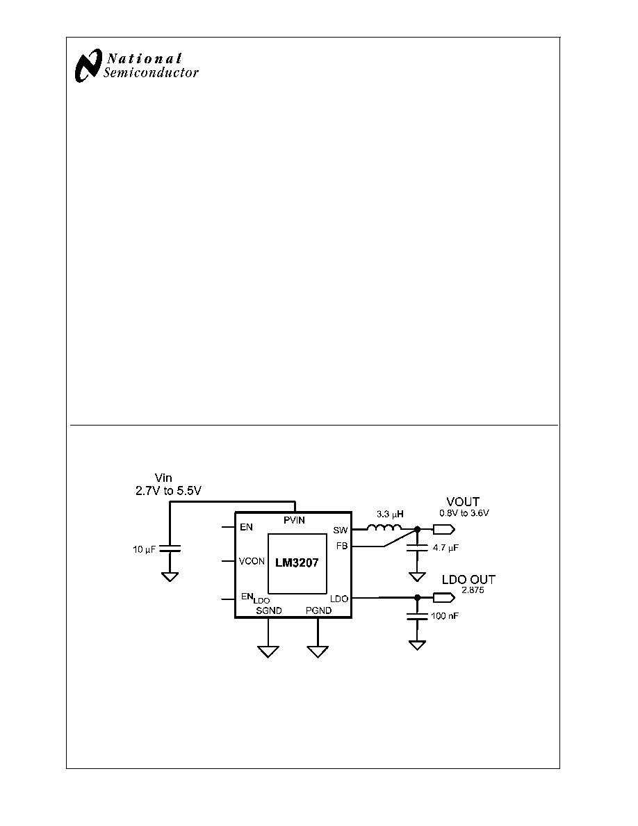
Typical Application
20165301
FIGURE 1. LM3207 Typical Application
August 2006
LM3207
650mA
Miniature,
Adjustable,
Step-Down
DC-DC
Converter
for
RF
Power
Amplifiers
© 2006 National Semiconductor Corporation
DS201653
www.national.com
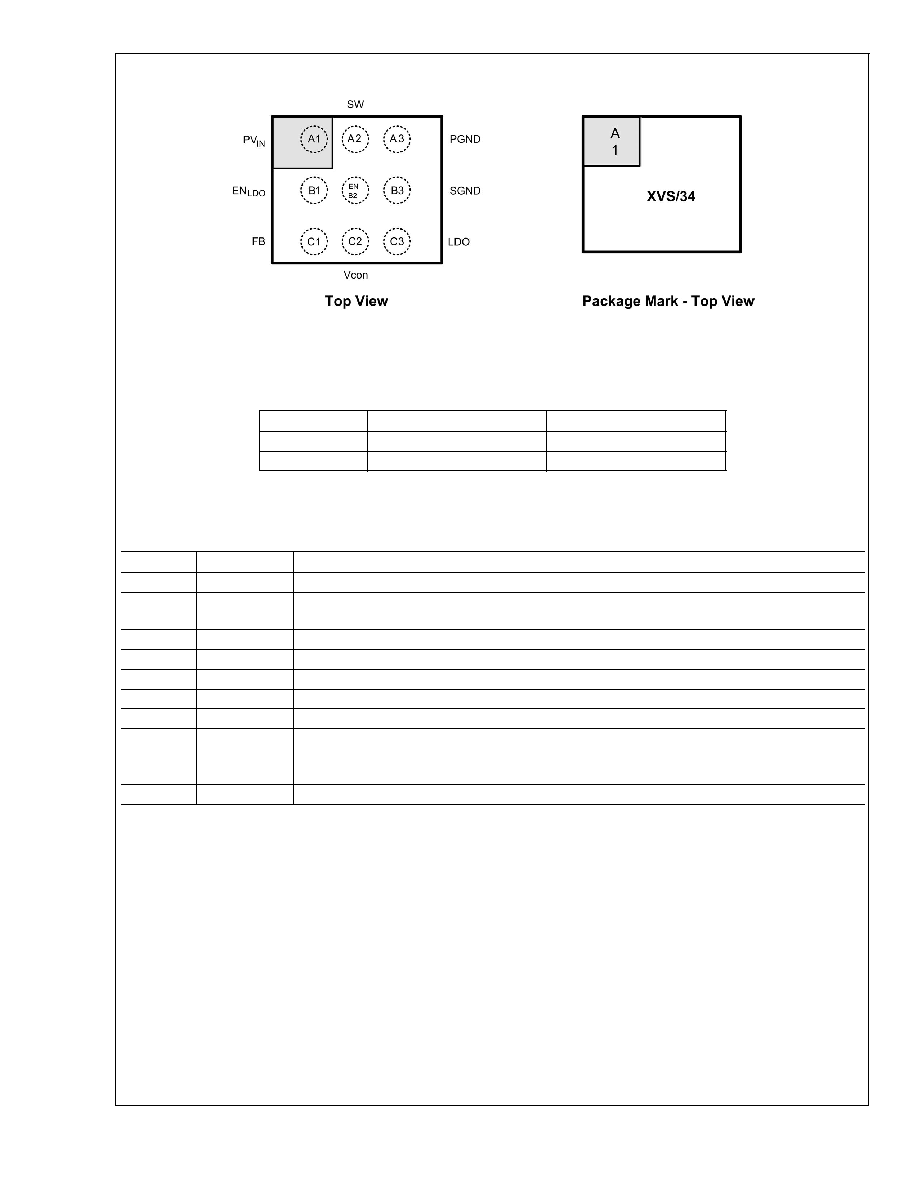
Connection Diagrams
20165399
9≠Bump Thin Micro SMD Package, Large Bump
NS Package Number TLA09TTA
Order Information
Order Number
Package Marking (Note)
Supplied As
LM3207TL
XVS/34
250 units, Tape-and-Reel
LM3207TLX
XVS/34
3000 units, Tape-and-Reel
Note: The actual physical placement of the package marking will vary from part to part. The package marking "X" designates the date
code. "V" is a NSC internal code for die traceability. "S" designates the device type as switcher device. Both will vary considerably. "34"
identifies the device (part number, option, etc.).
Pin Descriptions
Pin #
Name
Description
A1
PV
IN
Power Supply Voltage Input.
B1
EN
LDO
LDO Enable Input. Set this digital input high to turn on LDO (EN pin must also be set high). For
shutdown, set low.
C1
FB
Feedback Analog Input. Connect to the output at the output filter capacitor.
C2
V
CON
Voltage Control Analog input. V
CON
controls V
OUT
in PWM mode.
C3
LDO
LDO Output Voltage.
B3
SGND
Analog and Control Ground.
A3
PGND
Power Ground.
A2
SW
Switch node connection to the internal PFET switch and NFET synchronous rectifier. Connect to
an inductor with a saturation current rating that exceeds the maximum Switch Peak Current Limit
specification of the LM3207.
B2
EN
PWM enable Input. Set this digital input high for normal operation. For shutdown, set low.
LM3207
www.national.com
2
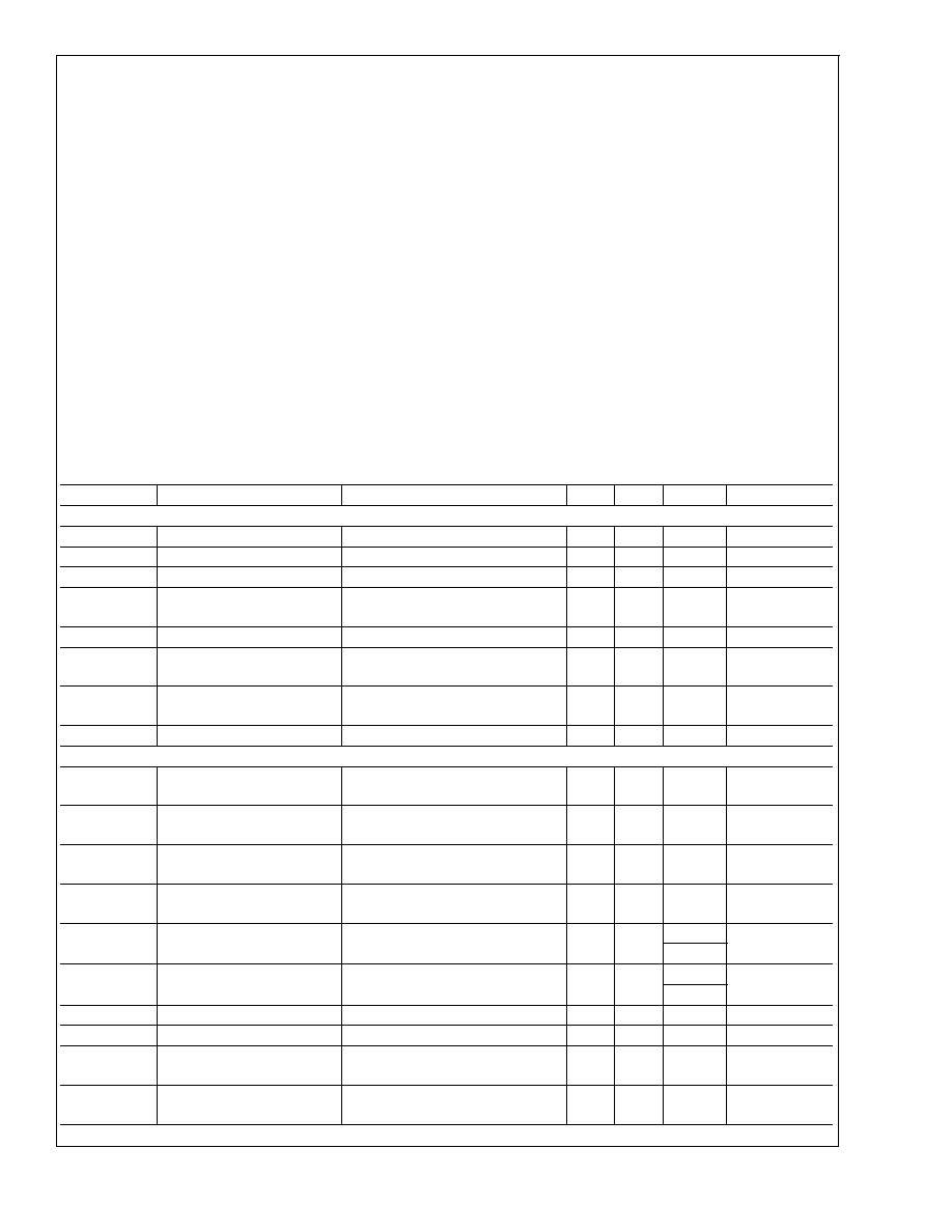
Absolute Maximum Ratings
(Notes 1, 2)
If Military/Aerospace specified devices are required,
please contact the National Semiconductor Sales Office/
Distributors for availability and specifications.
PV
IN
to SGND
-0.2V to +6.0V
PGND to SGND
-0.2V to +0.2V
EN, FB, V
CON
, EN
LDO
, LDO
(SGND -0.2V)
to (V
DD
+0.2V)
w/6.0V max
SW
(PGND -0.2V)
to (PV
IN
+0.2V)
w/6.0V max
PV
IN
-0.2V to +0.2V
Continuous Power Dissipation
(Note 3)
Internally Limited
Junction Temperature (T
J-MAX
)
+150∞C
Storage Temperature Range
-65∞C to +150∞C
Maximum Lead Temperature
(Soldering, 10 sec)
+260∞C
Operating Ratings
(Notes 1, 2)
Input Voltage Range
2.7V to 5.5V
Recommended Load Current
0mA to 650mA
Junction Temperature (T
J
) Range
-30∞C to +125∞C
Ambient Temperature (T
A
) Range
(Note 4)
-30∞C to +85∞C
Thermal Properties
Junction-to-Ambient Thermal
100∞C/W
Resistance (
JA
), TLA09 Package
(Note 5)
Electrical Characteristics
(Notes 2, 6, 7) Limits in standard typeface are for T
A
= T
J
= 25∞C. Limits in bold-
face type apply over the full operating ambient temperature range (-30∞C
T
A
= T
J
+85∞C). Unless otherwise noted, all
specifications apply to LM3207 with: PV
IN
= V
IN
= EN
LDO
= EN = 3.6V.
Symbol
Parameter
Conditions
Min
Typ
Max
Units
LDO
V
LDO
LDO Output Voltage
Iout = 0 mA
2.875
2.95
V
V
LDO,MIN
Minimum LDO Output Voltage Iout = 10mA, PV
IN
= 3V
2.80
V
I
SC
Short circuit current(DC)
V
LDO
= 0
50
mA
I
PUT
Pull-up current (transient)
V
LDO
= V
LDO(nom)
/2, PV
IN
= 3V
(Note 12)
150
mA
I
PD
DC Pull-down current (DC)
V
LDO
= PV
IN
, EN
LDO
= 0
-50
mA
I
PDT
Pull-down current (transient)
V
LDO
= V
LDO(nom)
/2, PV
IN
= 3V
(Note 12)
-200
mA
I
Q_LDO + PWM
DC Bias current into PV
IN
V
CON
= 2V, FB = 0V, No Switching,
EN
LDO
= EN = 3.6V (Note 9)
1.2
1.6
mA
I
PIN,ENLDO
LDO Pin pull down current
5
10
uA
Switcher
V
FB, MIN
Feedback Voltage at
minimum setting
V
CON
= 0.32V
0.75
0.8
0.85
V
V
FB, MAX
Feedback Voltage at
maximum setting
V
CON
= 1.44V, PV
IN
= 4.2V
3.537
3.6
3.683
V
I
SHDN
Shutdown supply current
EN = EN
LDO
= SW = V
CON
= 0V,
(Note 8)
0.01
2
µA
I
Q_PWM
DC bias current into PV
IN
V
CON
= 2V, FB = 0V, EN
LDO
= 0V ,
EN = 3.6V, No Switching (Note 9)
1.1
1.6
mA
R
DSON(P)
Pin-pin resistance for PFET
I
SW
= 200mA
140
200
m
230
R
DSON(N)
Pin-pin resistance for NFET
I
SW
= - 200mA
300
415
m
485
I
LIM,PFET
Switch peak current limit
(Note 10)
935
1100
1200
mA
F
OSC
Internal oscillator frequency
1.7
2
2.3
MHz
V
IH,EN
Logic high input threshold
(PWM, LDO)
1.2
V
V
IL,EN
Logic low input threshold
(PWM, LDO)
0.5
V
LM3207
www.national.com
3
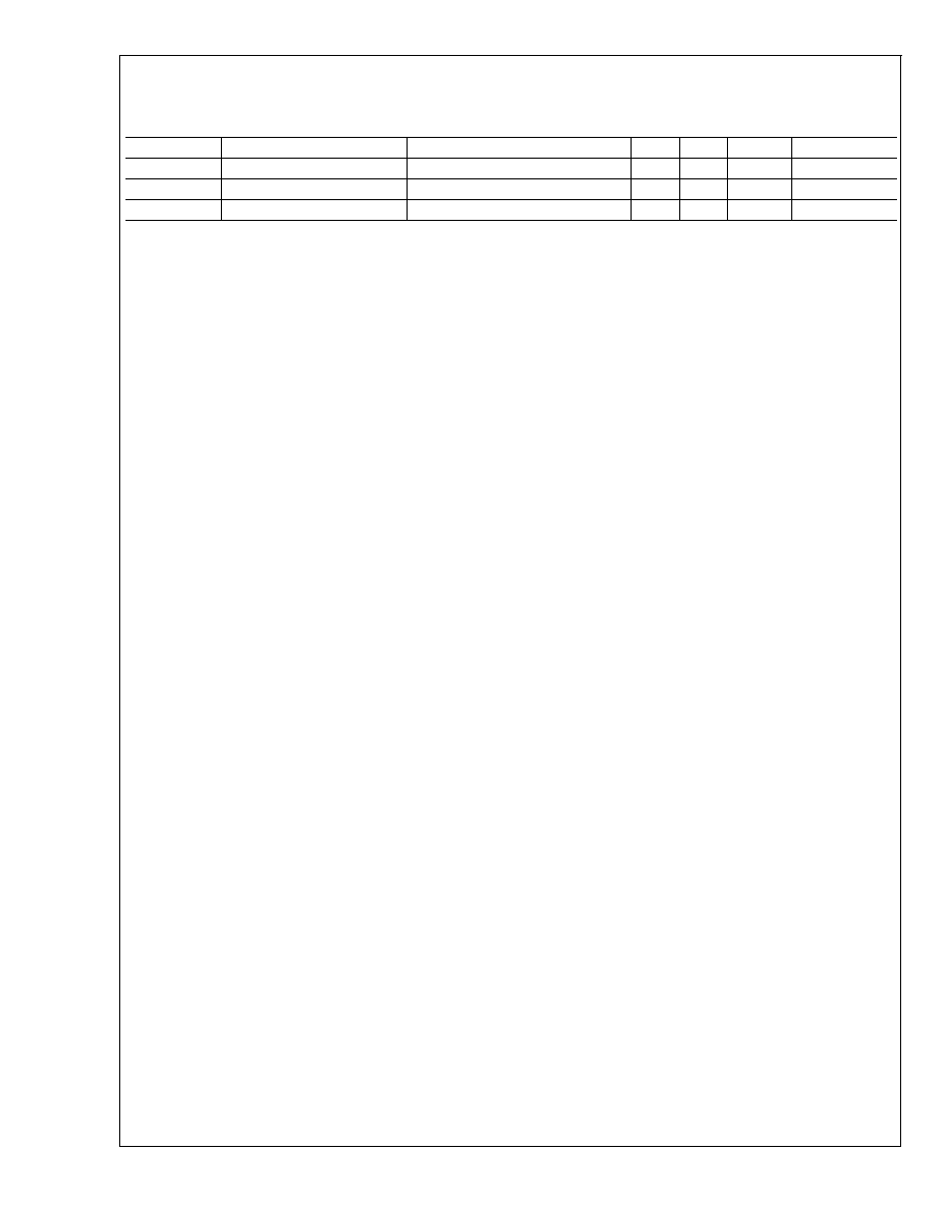
Electrical Characteristics
(Notes 2, 6, 7) Limits in standard typeface are for T
A
= T
J
= 25∞C. Limits in
boldface type apply over the full operating ambient temperature range (-30∞C
T
A
= T
J
+85∞C). Unless otherwise noted, all
specifications apply to LM3207 with: PV
IN
= V
IN
= EN
LDO
= EN = 3.6V. (Continued)
Symbol
Parameter
Conditions
Min
Typ
Max
Units
I
PIN,EN
PWM Pin pull down current
5
10
µA
Gain
V
CON
to V
OUT
Gain
0.32V
V
CON
1.44V
2.5
V/V
I
CON
V
CON
pin leakage current
V
CON
= 1.0V
±
1
µA
LM3207
www.national.com
4

System Characteristics
The following spec table entries are guaranteed by design providing the component
values in the typical application circuit are used (L = 3.0µH, (DCR = 0.12
, FDK MIPW3226D3R0M);
C
IN
= 10µF, (6.3V, 0805, TDK C2012X5R0J106K); C
OUT
= 4.7µF, (6.3V, 0603, TDK C1608X5R0J475M); C
LDO
= 100nF,
(10V, 0402, TDK C1005X5R1A104KT) (or 220nF, (6.3V, 0402, TDK C1005X5R0J224KT))) . These parameters are not
guaranteed by production testing. Min and Max values are specified over the V
IN
range = 2.7V to 5.5V and over the ambi-
ent temp range T
A
= -30∞C to 85∞C unless otherwise specified. Typical values are specified at PV
IN
= EN = 3.6V and T
A
=
25∞C unless otherwise specified.
Symbol
Parameter
Conditions
Min
Typ
Max
Units
LDO
PSRR
Power Supply Rejection
Ratio
Offset Freq = 1Khz, C
out
= 100nF,
I
out
= 1mA, PV
in
= Vout
(nom)
+ 0.5V
50
dB
V
LDO(NOISE)
Output Noise Voltage
BW = 10Hz to 100Khz, I
out
= 1mA
30
uVrms
t
LDO, ON
Time to reach 90% of
V
LDO(nom)
after EN
LDO
signal goes high.
C
LDO
= 100nF, PWM mode assumed to
be fully functional before EN
LDO
goes
high. PV
in
= 3V, Iout = 5 mA (Note 12)
3
uS
C
LDO
= 220nF, PWM mode assumed to
be fully functional before EN
LDO
goes
high. PV
in
= 3V, Iout = 5 mA (Note 12)
5
uS
t
LDO, OFF
Time to reach 10% of
V
LDO(nom)
after EN
LDO
signal goes low.
C
LDO
= 100nF, PV
in
= 3V, Iout = 0mA
(Note 12)
3
uS
C
LDO
= 220nF, PV
in
= 3V, Iout = 0mA
(Note 12)
5
Switcher
T
RESPONSE
(Rise time)
Time for V
OUT
to rise
from 0.8V to 3.6V
PV
IN
= 4.2V, C
OUT
= 4.7uF, L = 3.0uH,
R
LOAD
= 5.5
20
30
µs
T
RESPONSE
(Fall
time)
Time for V
OUT
to fall
from 3.6V to 0.8V
PV
IN
= 4.2V, C
OUT
= 4.7uF, L = 3.0uH,
R
LOAD
= 10
20
30
µs
C
CON
V
CON
input capacitance
V
CON
= 1V,
Test frequency = 100 kHz
20
pF
V
CON
Linearity
Linearity in control
range 0.32V to 1.44V
PV
IN
= 3.9V, Monotonic in nature
-3
+3
%
T
_ON
Turn on time
(time for output to reach
3.6V from Enable low to
high transition)
EN = Low to High, PV
IN
= 4.2V,
V
O
= 3.6V, C
OUT
= 4.7µF,
I
OUT
1mA
70
100
µs
Efficiency
(L = 3.0µH, DCR
100m
)
PV
IN
= 3.6V, V
OUT
= 0.8V, I
OUT
= 90mA
81
%
PV
IN
= 3.9V, V
OUT
= 3.4V, I
OUT
= 400mA
95
%
V
O_ripple
Ripple voltage, PWM
mode
PV
IN
= 3V to 4.5V, V
OUT
= 0.8V,
I
OUT
= 10mA to 400mA, (Note 11)
10
mVp-p
Line_tr
Line transient response
PV
IN
= 600mV perturbance,
T
RISE
= T
FALL
= 10µs, V
OUT
= 0.8V,
I
OUT
= 100mA
50
mV
Load_tr
Load transient response PV
IN
= 3.1/3.6/4.5V, V
OUT
= 0.8V,
transients up to 100mA,
T
RISE
= T
FALL
= 10µs
50
mV
Note 1: Absolute Maximum Ratings indicate limits beyond which damage to the component may occur. Operating Ratings are conditions under which operation of
the device is guaranteed. Operating Ratings do not imply guaranteed performance limits. For guaranteed performance limits and associated test conditions, see the
Electrical Characteristics tables.
Note 2: All voltages are with respect to the potential at the GND pins. The LM3207 is designed for mobile phone applications where turn-on after power-up is
controlled by the system controller and where requirements for a small package size overrule increased die size for internal Under Voltage Lock-Out (UVLO) circuitry.
Thus, it should be kept in shutdown by holding the EN pin low until the input voltage exceeds 2.7V.
Note 3: Internal thermal shutdown circuitry protects the device from permanent damage. Thermal shutdown engages at T
J
= 150∞C (typ.) and disengages at T
J
=
130∞C (typ.).
Note 4: In applications where high power dissipation and/or poor package thermal resistance is present, the maximum ambient temperature may have to be
de-rated. Maximum ambient temperature (T
A-MAX
) is dependent on the maximum operating junction temperature (T
J-MAX-OP
= 125∞C), the maximum power
dissipation of the device in the application (P
D-MAX
), and the junction-to ambient thermal resistance of the part/package in the application (
JA
), as given by the
following equation: T
A-MAX
= T
J-MAX-OP
≠ (
JA
x P
D-MAX
).
LM3207
www.national.com
5