LM3211
Step-up PWM DC/DC Converter Integrated with 4 Buffers
General Description
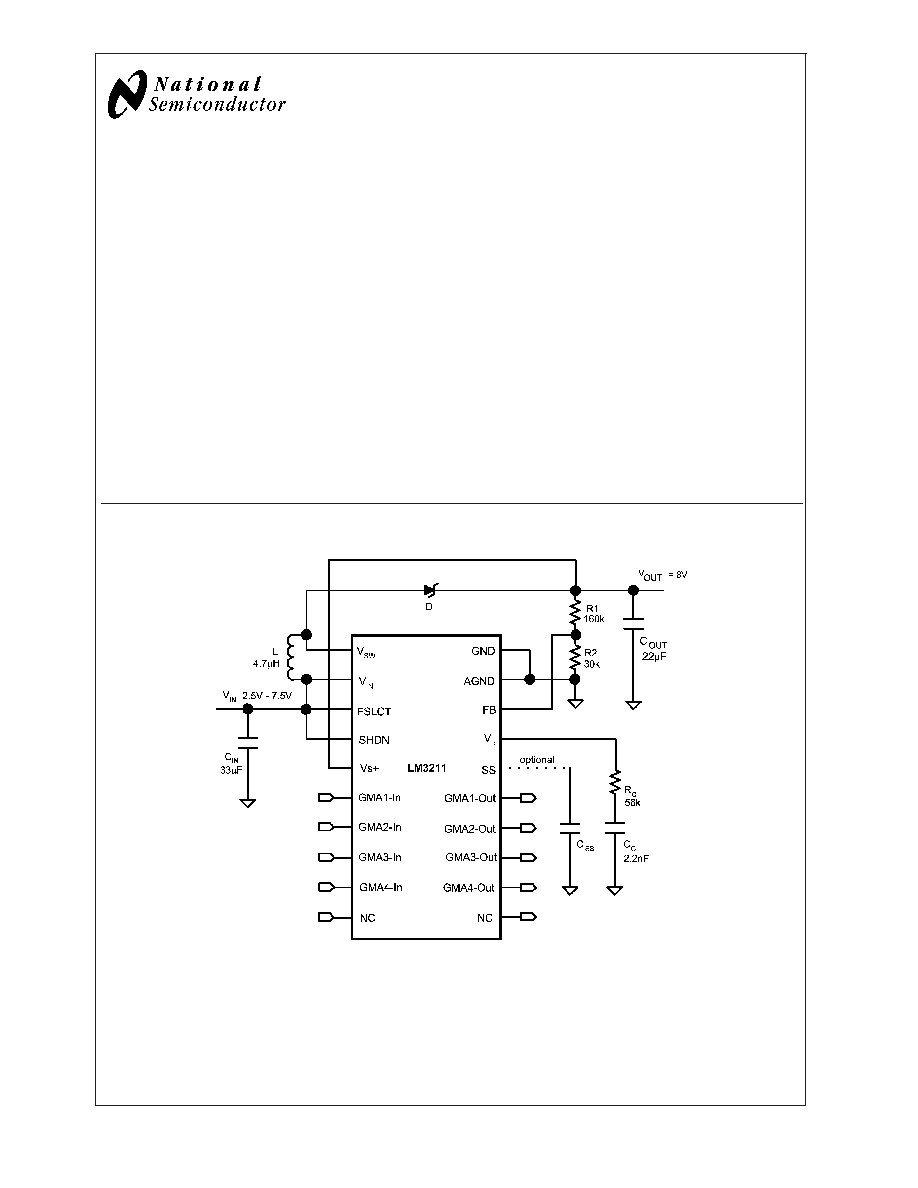
The LM3211 is a compact bias solution for TFT displays. It
has a current mode PWM step-up DC/DC converter with a
1.4A, 0.17
internal switch. Capable of generating 8V at
300mA from a Lithium Ion battery, the LM3211 is ideal for
generating bias voltages for large screen LCD panels. The
LM3211 can be operated at switching frequencies of 600kHz
or 1.25MHz, allowing for easy filtering and low noise. An
external compensation pin gives the user flexibility in setting
frequency compensation, which makes possible the use of
small, low ESR ceramic capacitors at the output. The
LM3211 uses a patented internal circuitry to limit startup
inrush current of the boost switching regulator without the
use of an external softstart capacitor. An external softstart
pin enables the user to tailor the softstart to a specific
application. The LM3211 contains 4 Gamma buffers capable
of supplying 35mA source and sink. The TSSOP-20 package
ensures a low profile overall solution.
Features
n
1.4A, 0.17
, internal power switch
n
V
IN
operating range: 2.2V to 7.5V
n
600kHz/1.25MHz selectable frequency step-up DC/DC
converter
n
20 pin TSSOP package
n
Inrush current limiting circuitry
n
External softstart override
n
4 Gamma buffers
Applications
n
LCD Bias Supplies
n
Handheld Devices
n
Portable Applications
n
Cellular Phones/Digital Cameras
Typical Application Circuit
20062231
February 2004
LM321
1
Step-up
PWM
DC/DC
Converter
Integrated
with
4
Buffers
© 2004 National Semiconductor Corporation
DS200622
www.national.com
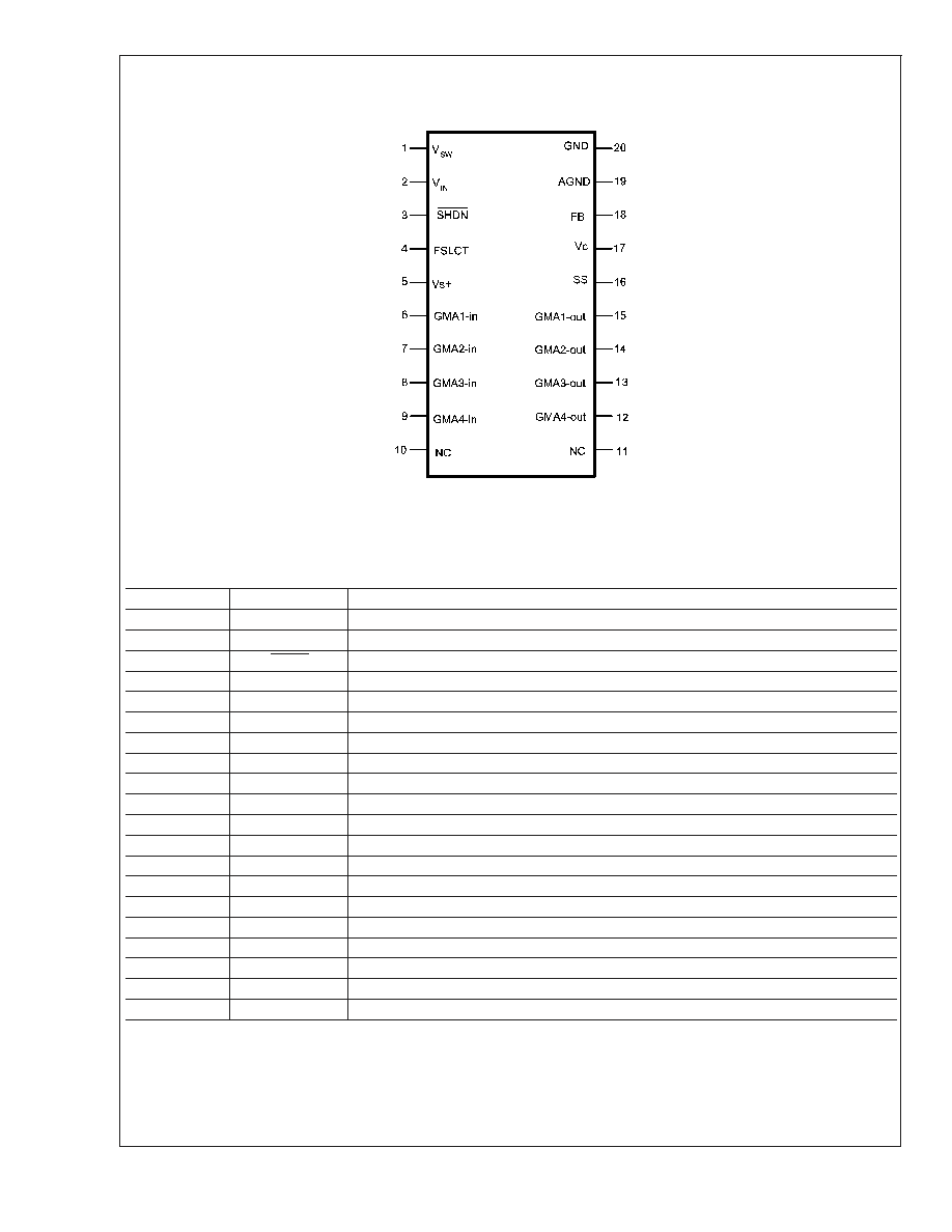
Connection Diagram
Top View
20062204
TSSOP 20 package
T
JMAX
= 125∞C,
JA
= 120∞C/W (Note 1)
Pin Description
Pin
Name
Function
1
V
SW
Power switch input.
2
V
IN
Switching Regulator Power input.
3
SHDN
Shutdown pin, active low.
4
FSLCT
Frequency Select pin. FSLCT = V
IN
for 1.25 MHz, FSLCT = AGND or floating for 600kHz.
5
Vs+
Gamma Buffer input supply.
6
GMA1-in
Gamma Buffer input.
7
GMA2-in
Gamma Buffer input.
8
GMA3-in
Gamma Buffer input.
9
GMA4-in
Gamma Buffer input.
10
NC
No Connection, leave open.
11
NC
No Connection, leave open.
12
GMA4-out
Gamma Buffer output.
13
GMA3-out
Gamma Buffer output.
14
GMA2-out
Gamma Buffer output.
15
GMA1-out
Gamma Buffer output.
16
SS
Soft start pin.
17
V
C
Boost Compensation Network Connection.
18
FB
Output Voltage Feedback input.
19
AGND
Gamma Buffer ground, Analog ground connection for Regulator.
20
GND
Switch Power Ground.
LM321
1
www.national.com
2
Pin Functions
V
SW
(Pin 1): This is the drain of the internal NMOS power
switch. Minimize the metal trace area connected to this pin to
minimize EMI.
V
IN
(Pin 2): Input Supply Pin. Bypass this pin with a capacitor
as close to the device as possible. The capacitor should
connect between V
IN
and GND.
SHDN(Pin 3): Shutdown Pin. The shutdown pin signal is
active low. A voltage of less than 0.3V disables the device. A
voltage greater than 0.85V enables the device.
FSLCT(Pin 4): Frequency Select Pin. Connecting FSLCT to
AGND selects a 600 kHz operating frequency for the switch-
ing regulator. Connecting FSLCT to V
IN
selects a 1.25 MHz
operating frequency. If FSLCT is left floating, the switching
frequency defaults to 600 kHz.
Vs+(Pin 5): Supply pin for the four Gamma buffers. Bypass
this pin with a capacitor as close to the device as possible.
The capacitor should connect between Vs+ and GND.
GMA1-in(Pin 6):Gamma Buffer input pin.
GMA2-in(Pin 7): Gamma Buffer input pin.
GMA3-in(Pin 8): Gamma Buffer input pin.
GMA4-in(Pin 9): Gamma Buffer input pin.
NC(Pin 10):No Connection.
NC(Pin 11): No Connection.
GMA4-out(Pin 12): Gamma Buffer output pin.
GMA3-out(Pin13): Gamma Buffer output pin.
GMA2-out(Pin 14): Gamma Buffer output pin.
GMA1-out(Pin 15): Gamma Buffer output pin.
SS(Pin 16): Softstart pin. Connect capacitor to SS pin and
AGND to slowly ramp inductor current on startup.
V
C
(Pin 17): Compensation Network for Boost switching
regulator. Connect resistor/capacitor network between V
C
pin and AGND for boost switching regulator AC compensa-
tion.
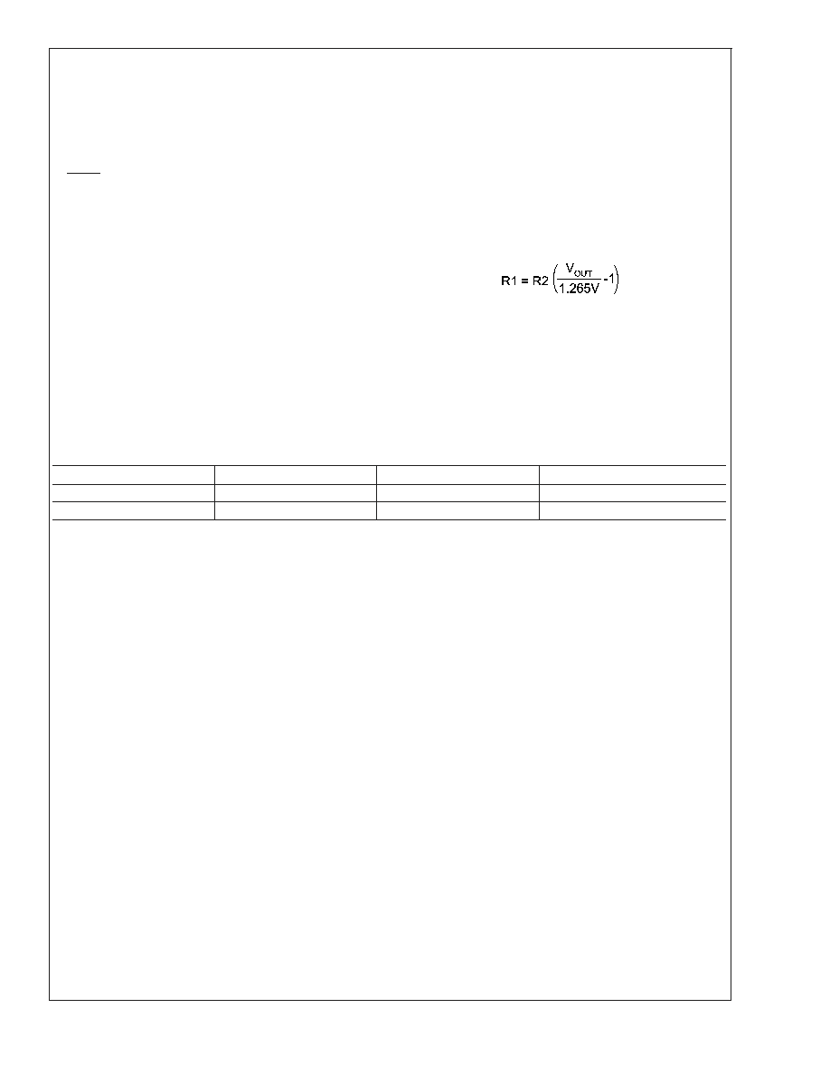
FB(Pin 18): Feedback pin. Set the output voltage by select-
ing values of R1 and R2 using:
Connect the ground of the feedback network to the AGND
plane, which can be tied directly to the GND pin.
AGND(Pin 19): Analog ground pin. Ground connection for
the Gamma buffers and the boost switching regulator. AGND
must be tied directly to GND at the pins.
GND(Pin 20): Power ground pin. Ground connection for the
NMOS power device of the boost switching regulator. GND
must be tied directly to AGND at the pins.
Ordering Information
Order Number
Package Type
NSC Package Drawing
Supplied As
LM3211MT-ADJ
TSSOP-20
MTC20
73 Units, Rail
LM3211MTX-ADJ
TSSOP-20
MTC20
2500 Units, Tape and Reel
LM321
1
www.national.com
3
Absolute Maximum Ratings
(Note 2)
If Military/Aerospace specified devices are required,
please contact the National Semiconductor Sales Office/
Distributors for availability and specifications.
V
IN
-0.3V to 7.5V
V
SW
Voltage
-0.3V to 18V
FB Voltage
-0.3V to 7V
V
C
Voltage
0.965V to 1.565V
SHDN Voltage
-0.3V to V
IN
FSLCT Voltage
AGND to V
IN
Supply Voltage, Vs+
-0.3V to 14V
Buffer Input Voltage
Rail-to-Rail
Buffer Output Voltage
Rail-to-Rail
ESD Ratings
(Note 3)
Human Body Model
2kV
Machine Model
150V
Operating Conditions
Operating Temperature
-40∞C to +125∞C
Storage Temperature
-65∞C to +150∞C
Supply Voltage, V
IN
2.2V to 7.5V
V
SW
Voltage
17V
Supply Gamma Buffer, Vs+
4V to 14V
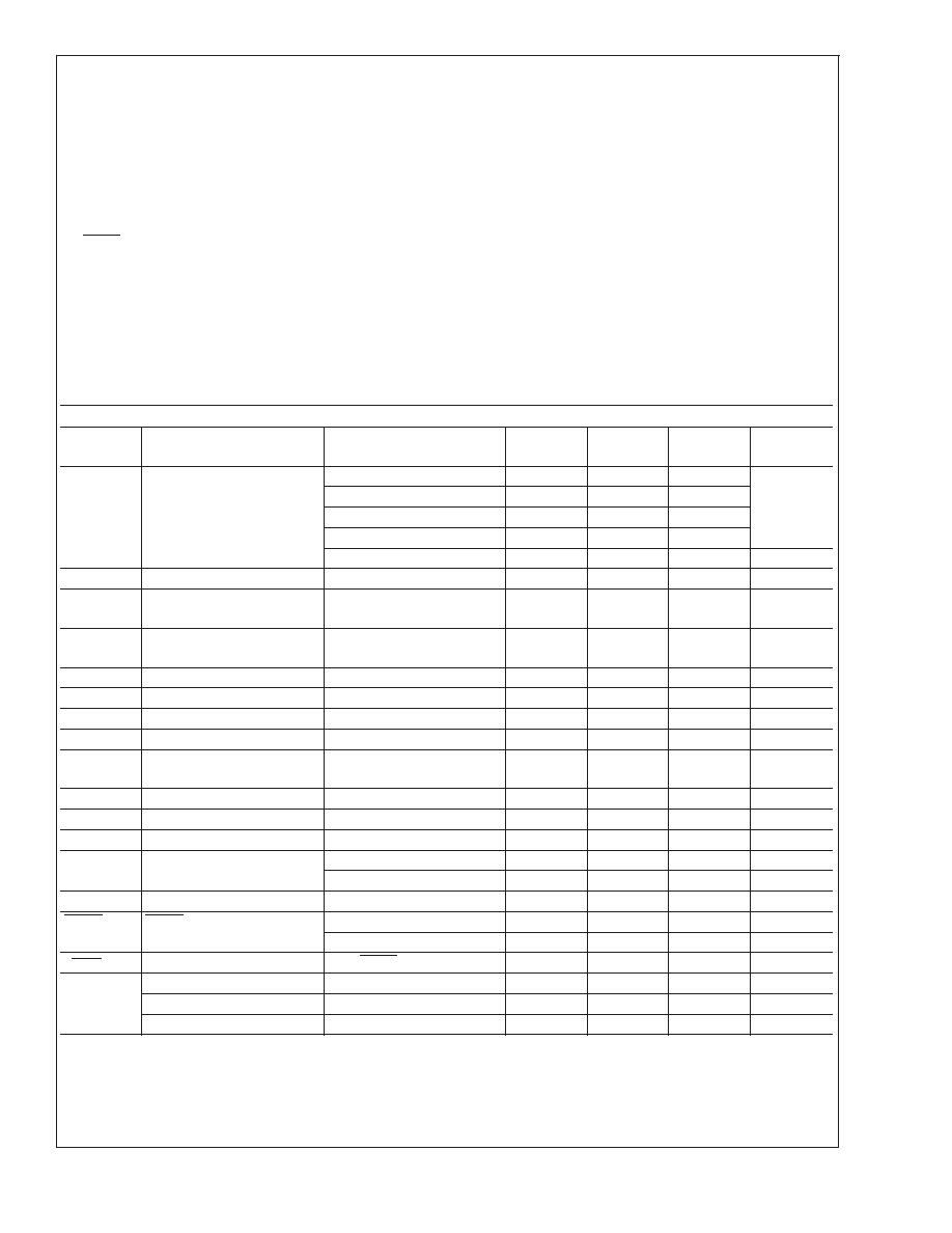
Electrical Characteristics
Specifications in standard type face are for T
J
= 25∞C and those with boldface type apply over the full Operating Tempera-
ture Range ( T
J
= -40∞C to +125∞C). Unless otherwise specified, V
IN
=2.2V and Vs+ = 8V.
Switching Regulator
Symbol
Parameter
Conditions
Min
(Note 4)
Typ
(Note 5)
Max
(Note 4)
Units
I
Q
Quiescent Current
Not Switching, FSCLT = 0V
1.6
2
mA
Not Switching, FSCLT = V
IN
1.65
2.2
Switching, FSCLT = 0V
2.5
3
Switching, FSCLT = V
IN
3.4
4
Shutdown mode
6
15
µA
V
FB
Feedback Voltage
1.239
1.265
1.291
V
%V
FB
/
V
IN
Feedback Voltage Line
Regulation
0.03
0.05
%/V
I
CL
Switch Current Limit
(Note 6)
V
IN
= 2.5V, V
OUT
= 8V
1.4
A
R
DSON
Switch R
DSON
(Note 7)
V
IN
= 2.7V
170
m
I
B
FB Pin Bias Current(Note 8)
30
90
nA
V
IN
Input Voltage Range
2.2
7.5
V
I
SS
Soft Start Current
5
11
15
µA
T
SS
Internal Soft Start Ramp
Time
FSLCT = 0V
6.7
12
mS
g
m
Error Amp Transconductance
I = 5µA
60
135
250
µmho
A
V
Error Amp Voltage Gain
135
V/V
D
MAX
Maximum Duty Cycle
78
85
%
f
S
Switching Frequency
FSLCT = 0V
500
600
700
kHz
FSLCT = V
IN
0.9
1.25
1.5
MHz
I
L
Switch Leakage Current
V
SW
= 17V
0.185
20
µA
SHDN
SHDN Threshold
Output High
0.85
0.6
V
Output Low
0.6
0.3
V
I
SHDN
Shutdown Pin Current
0V
SHDN V
IN
0.5
1
µA
UVP
On Threshold
1.8
1.9
2
V
Off Threshold
1.7
1.8
1.9
V
Hysteresis
100
mV
LM321
1
www.national.com
5