 | –≠–ª–µ–∫—Ç—Ä–æ–Ω–Ω—ã–π –∫–æ–º–ø–æ–Ω–µ–Ω—Ç: LM330-5 | –°–∫–∞—á–∞—Ç—å:  PDF PDF  ZIP ZIP |
LM330
3-Terminal Positive Regulator
General Description
The LM330 5V 3-terminal positive voltage regulator features
an ability to source 150 mA of output current with an
input-output differential of 0.6V or less. Familiar regulator
features such as current limit and thermal overload protec-
tion are also provided.
The low dropout voltage makes the LM330 useful for certain
battery applications since this feature allows a longer battery
discharge before the output falls out of regulation. For ex-
ample, a battery supplying the regulator input voltage may
discharge to 5.6V and still properly regulate the system and
load voltage. Supporting this feature, the LM330 protects
both itself and regulated systems from negative voltage in-
puts resulting from reverse installations of batteries.
Other protection features include line transient protection up
to 26V, when the output actually shuts down to avoid damag-
ing internal and external circuits. Also, the LM330 regulator
cannot be harmed by a temporary mirror-image insertion.
Features
n
Input-output differential less than 0.6V
n
Output current of 150 mA
n
Reverse battery protection
n
Line transient protection
n
Internal short circuit current limit
n
Internal thermal overload protection
n
Mirror-image insertion protection
n
P
+
Product Enhancement tested
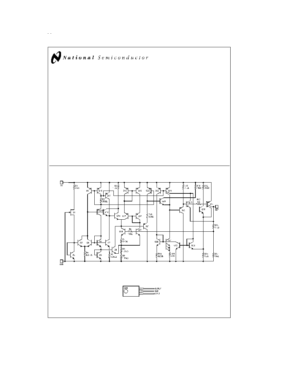
Schematic and Connection Diagrams
DS009306-1
(TO-220)
Plastic Package
DS009306-2
Front View
Order Number LM330T-5.0
See NS Package Number T03B
May 1998
LM330
3-T
erminal
Positive
Regulator
© 1999 National Semiconductor Corporation
DS009306
www.national.com
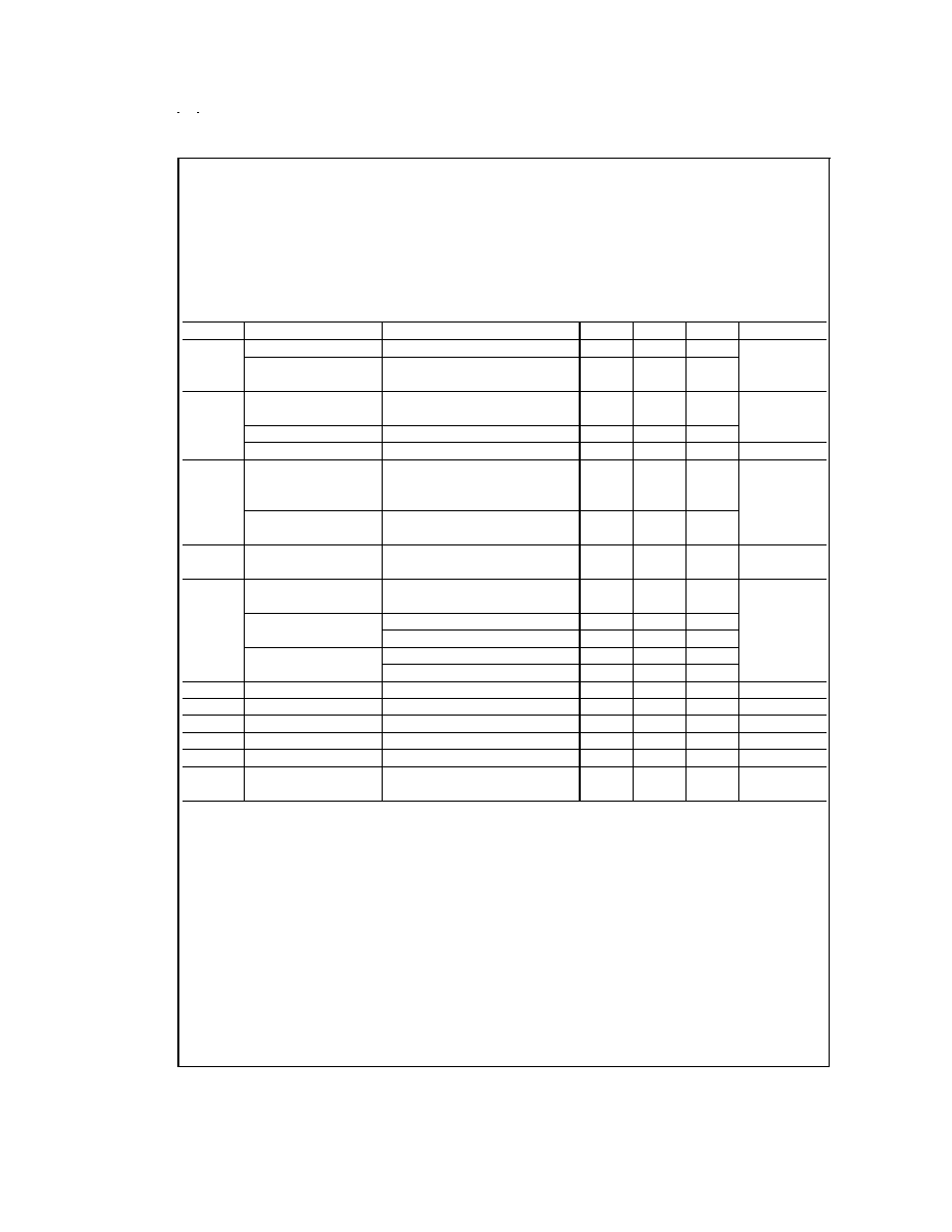
Absolute Maximum Ratings
(Note 1)
If Military/Aerospace specified devices are required,
please contact the National Semiconductor Sales Office/
Distributors for availability and specifications.
Input Voltage
Operating Range
26V
Line Transient Protection (1000 ms)
40V
Internal Power Dissipation
Internally Limited
Operating Temperature Range
0∞C to +70∞C
Maximum Junction Temperature
+125∞C
Storage Temperature Range
-65∞C to +150∞C
Lead Temperature
(Soldering, 10 sec.)
+300∞C
Electrical Characteristics
(Note 2)
Symbol
Parameter
Conditions
Min
Typ
Max
Units
V
o
Output Voltage
T
j
= 25∞C
4.8
5
5.2
Output Voltage
5
<
I
o
<
150 mA
4.75
5.25
V
Over Temp
6
<
V
IN
<
26V; 0∞C
T
j
100∞C
V
o
Line Regulation
9
<
V
IN
<
16V, I
o
= 5 mA
7
25
6
<
V
IN
<
26V, I
o
= 5 mA
30
60
mV
Load Regulation
5
<
I
o
<
150 mA
14
50
Long Term Stability
20
mV/1000 hrs
I
Q
Quiescent Current
I
o
= 10 mA
3.5
7
I
o
= 50 mA
5
11
I
o
= 150 mA
18
40
mA
Line Transient
V
IN
= 40V, R
L
= 100
, 1s
14
Reverse Polarity
V
IN
= -6V, R
L
= 100
-80
I
Q
Quiescent Current
6
<
V
IN
<
26V
10
%
Change
V
IN
Overvoltage Shutdown
26
38
Voltage
Max Line Transient
60
V
1s, V
o
5.5V
50
Reverse Polarity
-30
Input Voltage
DC V
o
>
- 0.3V, R
L
= 100
-12
Output Noise Voltage
10 Hz≠100 kHz
50
µV
Output Impedance
I
o
= 100 mADC + 10 mArms
200
m
Ripple Rejection
56
dB
Current Limit
150
400
700
mA
Dropout Voltage
I
o
= 150 mA
0.32
0.6
V
Thermal Resistance
Junction to Case
4
∞C/W
Junction to Ambient
50
Note 1: "Absolute Maximum Ratings" indicate limits beyond which damage to the device may occur. Operating Ratings indicate conditions for which the device is
functional, but do not guarantee specific performance limits.
Note 2: Unless otherwise specified: V
IN
= 14V, I
o
= 150 mA, T
j
= 25∞C, C1 = 0.1 µF, C2 = 10 µF. All characteristics except noise voltage and ripple rejection are
measured using pulse techniques (t
W
10 ms, duty cycle
5%). Output voltage changes due to changes in internal temperature must be taken into account sepa-
rately.
www.national.com
2
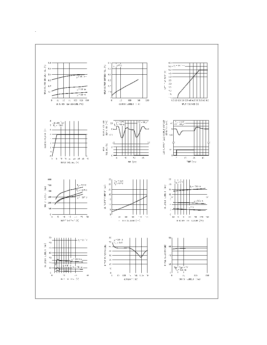
Typical Performance Characteristics
Dropout Voltage
DS009306-7
Dropout Voltage
DS009306-8
Low Voltage Behavior
DS009306-9
High Voltage Behavior
DS009306-10
Line Transient Response
DS009306-11
Load Transient Response
DS009306-12
Peak Output Current
DS009306-13
Quiescent Current
DS009306-14
Quiescent Current
DS009306-15
Quiescent Current
DS009306-16
Ripple Rejection
DS009306-17
Ripple Rejection
DS009306-18
www.national.com
3
Typical Performance Characteristics
(Continued)
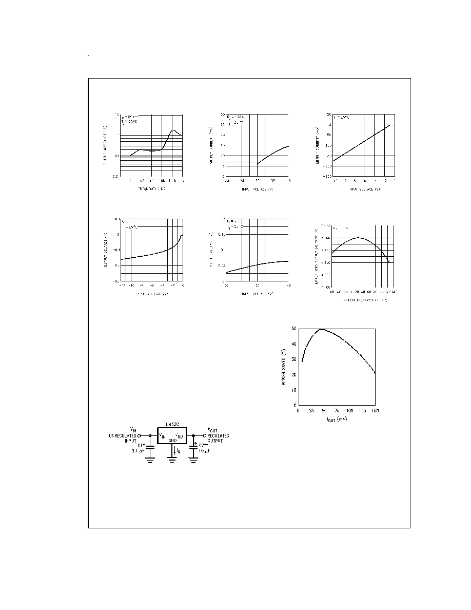
Typical Applications
The LM330 is designed specifically to operate at lower input
to output voltages. The device is designed utilizing a power
lateral PNP transistor which reduces dropout voltage from
2.0V to 0.3V when compared to IC regulators using NPN
pass transistors. Since the LM330 can operate at a much
lower input voltage, the device power dissipation is reduced,
heat sinking can be simpler and device reliability improved
through lower chip operating temperature. Also, a cost sav-
ings can be utilized through use of lower power/voltage com-
ponents. In applications utilizing battery power, the LM330
allows the battery voltage to drop to within 0.3V of output
voltage prior to the voltage regulator dropping out of regula-
tion.
Output Impedance
DS009306-19
Overvoltage Supply Current
DS009306-20
Reverse Supply Current
DS009306-21
Output at Reverse Supply
DS009306-22
Output at Overvoltage
DS009306-23
Output Voltage (Normalized
to 5V at T
j
= 25∞C)
DS009306-24
DS009306-5
*
Required if regulator is located far from power supply filter.
**
C2 may be either an Aluminum or Tantalum type capacitor but must be
rated to operate at -40∞C to guarantee regulator stability to that
temperature extreme. 10 µF is the minimum value required for stability and
may be increased without bound. Locate as close as possible to the
regulation.
DS009306-6
Note: Compared to IC regulator with 2.0V dropout voltage and
I
Qmax
, = 6.0 mA.
www.national.com
4

Physical Dimensions
inches (millimeters) unless otherwise noted
LIFE SUPPORT POLICY
NATIONAL'S PRODUCTS ARE NOT AUTHORIZED FOR USE AS CRITICAL COMPONENTS IN LIFE SUPPORT
DEVICES OR SYSTEMS WITHOUT THE EXPRESS WRITTEN APPROVAL OF THE PRESIDENT AND GENERAL
COUNSEL OF NATIONAL SEMICONDUCTOR CORPORATION. As used herein:
1. Life support devices or systems are devices or
systems which, (a) are intended for surgical implant
into the body, or (b) support or sustain life, and
whose failure to perform when properly used in
accordance with instructions for use provided in the
labeling, can be reasonably expected to result in a
significant injury to the user.
2. A critical component is any component of a life
support device or system whose failure to perform
can be reasonably expected to cause the failure of
the life support device or system, or to affect its
safety or effectiveness.
National Semiconductor
Corporation
Americas
Tel: 1-800-272-9959
Fax: 1-800-737-7018
Email: support@nsc.com
National Semiconductor
Europe
Fax: +49 (0) 1 80-530 85 86
Email: europe.support@nsc.com
Deutsch Tel: +49 (0) 1 80-530 85 85
English
Tel: +49 (0) 1 80-532 78 32
FranÁais Tel: +49 (0) 1 80-532 93 58
Italiano
Tel: +49 (0) 1 80-534 16 80
National Semiconductor
Asia Pacific Customer
Response Group
Tel: 65-2544466
Fax: 65-2504466
Email: sea.support@nsc.com
National Semiconductor
Japan Ltd.
Tel: 81-3-5639-7560
Fax: 81-3-5639-7507
www.national.com
TO Plastic Package
Order Number LM330T-5.0
NS Package Number T03B
LM330
3-T
erminal
Positive
Regulator
National does not assume any responsibility for use of any circuitry described, no circuit patent licenses are implied and National reserves the right at any time without notice to change said circuitry and specifications.