 | –≠–ª–µ–∫—Ç—Ä–æ–Ω–Ω—ã–π –∫–æ–º–ø–æ–Ω–µ–Ω—Ç: LM3310SQ | –°–∫–∞—á–∞—Ç—å:  PDF PDF  ZIP ZIP |
LM3310
Step-up PWM DC/DC Converter with Integrated Op-Amp
and Gate Pulse Modulation Switch
General Description
The LM3310 is a step-up DC/DC converter integrated with
an Operational Amplifier and a gate pulse modulation switch.
The boost (step-up) converter is used to generate an adjust-
able output voltage and features a low R
DSON
internal switch
for maximum efficiency. The operating frequency is select-
able between 660kHz and 1.28MHz allowing for the use of
small external components. An external soft-start pin en-
ables the user to tailor the soft-start time to a specific appli-
cation and limit the inrush current. The Op-Amp is capable of
sourcing/sinking 135mA of current (typical). The gate pulse
modulation switch can operate with a VGH voltage of 5V to
30V. The LM3310 is available in a low profile 24-lead LLP
package.
Features
n
Boost converter with a 2A, 0.18
switch
n
Boost output voltage adjustable up to 20V
n
Operating voltage range of 2.5V to 7V
n
660kHz/1.28MHz pin selectable switching frequency
n
Adjustable soft-start function
n
Input undervoltage protection
n
Over temperature protection
n
Integrated Op-Amp
n
Integrated gate pulse modulation (GPM) switch
n
24-Lead LLP package
Applications
n
TFT Bias Supplies
n
Portable Applications
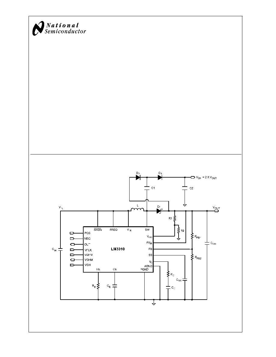
Typical Application Circuit
20133331
August 2005
LM3310
Step-up
PWM
DC/DC
Converter
with
Integrated
Op-Amp
and
Gate
Pulse
Modulation
Switch
© 2005 National Semiconductor Corporation
DS201333
www.national.com
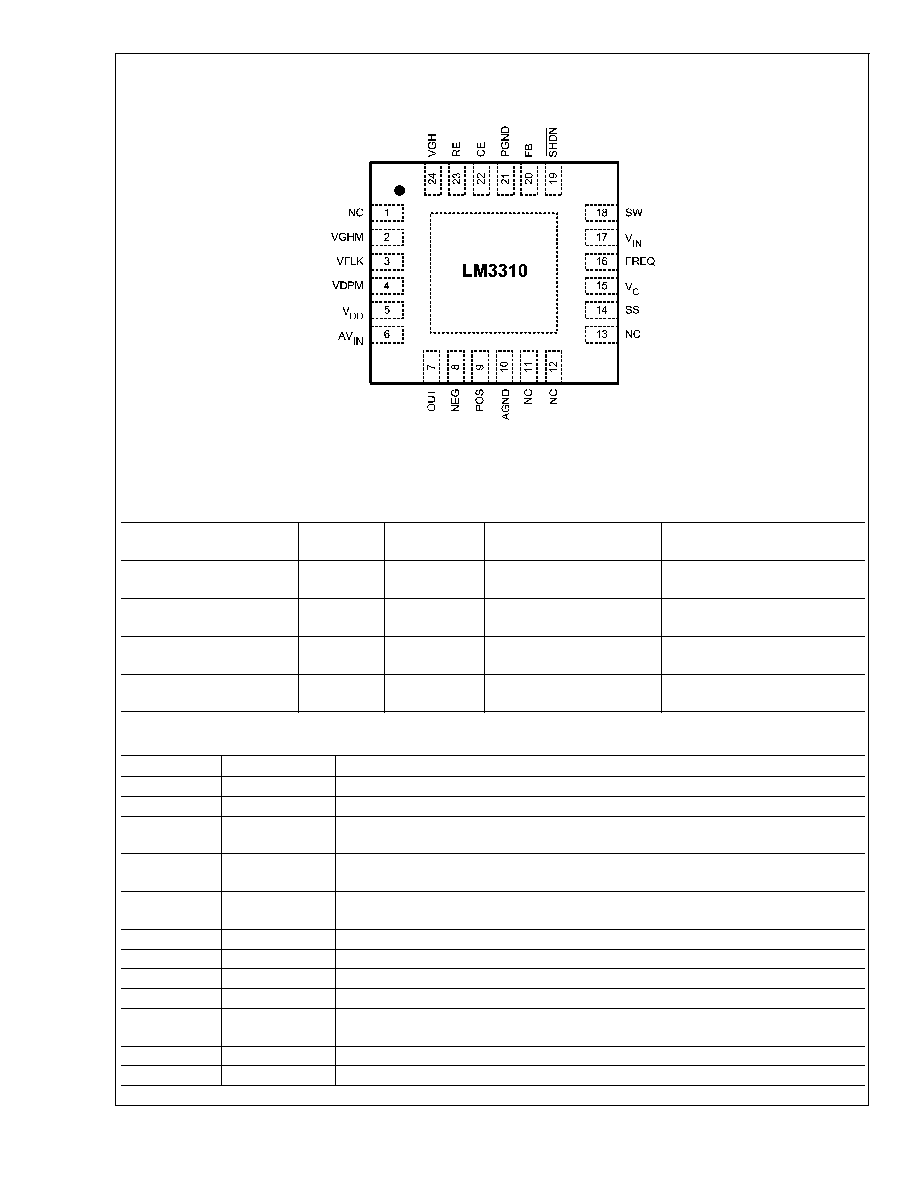
Connection Diagram
20133304
LLP-24 (Top View)
JA
=37∞C/W
Ordering Information
Order Number
Spec.
Package
Type
NSC Package Drawing
Supplied As
LM3310SQ
LLP-24
SQA24A
1000 units/reel
tape and reel
LM3310SQX
LLP-24
SQA24A
4500 units/reel
tape and reel
LM3310SQ
NOPB
LLP-24
SQA24A
1000 units/reel
tape and reel
LM3310SQX
NOPB
LLP-24
SQA24A
4500 units/reel
tape and reel
Pin Descriptions
Pin
Name
Function
1
NC
Not internally connected. Leave pin open.
2
VGHM
Output of GPM circuit. This output directly drives the supply for the gate driver circuits.
3
VFLK
Determines when the TFT LCD is on or off. This is controlled by the timing controller in
the LCD module.
4
VDPM
VDPM pin is the enable signal for the GPM block. Pulling this pin high enables the GPM
while pulling this pin low disables it. VDPM is used for timing sequence control.
5
V
DD
Reference input for gate pulse modulation (GPM) circuit. The voltage at V
DD
is used to set
the lower VGHM voltage.
6
AV
IN
Op-Amp analog power input.
7
OUT
Output of the Op-Amp.
8
NEG
Negative input terminal of the Op-Amp.
9
POS
Positive input terminal of the Op-Amp.
10
AGND
Analog ground for the step-up regulator, LDO, and Op-Amp. Connect directly to DAP and
PGND beneath the device.
11
NC
Not internally connected. Leave pin open.
12
NC
Not internally connected. Leave pin open.
LM3310
www.national.com
2
Pin Descriptions
(Continued)
Pin
Name
Function
13
NC
Not internally connected. Leave pin open.
14
SS
Boost converter soft start pin.
15
V
C
Boost compensation network connection. Connected to the output of the voltage error
amplifier.
16
FREQ
Switching frequency select input. Connect this pin to V
IN
for 1.28MHz operation and
AGND for 660kHz operation.
17
V
IN
Boost converter and GPM power input.
18
SW
Boost power switch input. Switch connected between SW pin and PGND pin.
19
SHDN
Shutdown pin. Active low, pulling this pin low disable the LM3310.
20
FB
Boost output voltage feedback input.
21
PGND
Power Ground. Source connection of the step-up regulator NMOS switch and ground for
the GPM circuit. Connect AGND and PGND directly to the DAP beneath the device.
22
CE
Connect capacitor from this pin to AGND.
23
RE
Connect a resistor between RE and PGND.
24
VGH
GPM power supply input. VGH range is 5V to 30V.
DAP
Die Attach Pad. Internally connected to GND. Connect AGND and PGND pins directly to
this pad beneath the device.
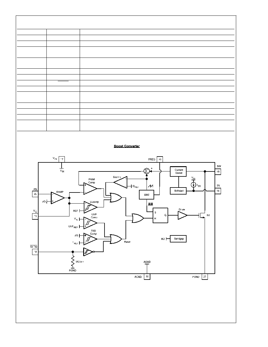
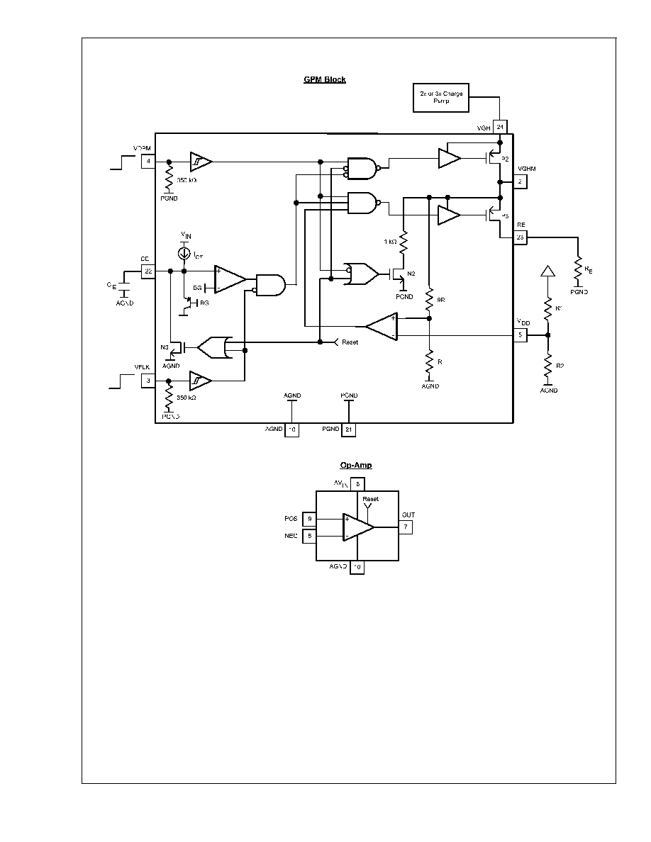
Block Diagrams
20133357
LM3310
www.national.com
3
Block Diagrams
(Continued)
20133358
20133359
LM3310
www.national.com
4
Absolute Maximum Ratings
(Note 1)
If Military/Aerospace specified devices are required,
please contact the National Semiconductor Sales Office/
Distributors for availability and specifications.
V
IN
7.5V
SW Voltage
21V
FB Voltage
V
IN
V
C
Voltage (Note 2)
1.265V
±
0.3V
SHDN Voltage
7.5V
FREQ
V
IN
AV
IN
12V
Amplifier Inputs/Output
Rail-to-Rail
VGH Voltage
31V
VGHM Voltage
VGH
VFLK, VDPM, V
DD
Voltage
7.5V
CE Voltage (Note 2)
1.265 + 0.3V
RE Voltage
VGH
Maximum Junction
Temperature
150∞C
Power Dissipation(Note 3)
Internally Limited
Lead Temperature
300∞C
Vapor Phase (60 sec.)
215∞C
Infrared (15 sec.)
220∞C
ESD Susceptibility (Note 4)
Human Body Model
2kV
Operating Conditions
Operating Junction
Temperature Range (Note 5)
-40∞C to +125∞C
Storage Temperature
-65∞C to +150∞C
Supply Voltage
2.5V to 7V
Maximum SW Voltage
20V
VGH Voltage Range
5V to 30V
Op-Amp Supply, AV
IN
4V to 12V
Electrical Characteristics V
IN
=2.5V and I
L
= 0A
Specifications in standard type face are for T
J
= 25∞C and those with boldface type apply over the full Operating Tempera-
ture Range ( T
J
= -40∞C to +125∞C). Unless otherwise specified, V
IN
=2.5V and I
L
= 0A.
Symbol
Parameter
Conditions
Min(Note 5) Typ(Note 6) Max(Note 5)
Units
I
Q
Quiescent Current
FB = 2V (Not Switching)
690
1100
µA
V
SHDN
= 0V
0.04
0.5
8.5
660kHz Switching
2.1
2.8
mA
1.28MHz Switching
3.1
4.0
V
FB
Feedback Voltage
1.231
1.263
1.287
V
%V
FB
/
V
IN
Feedback Voltage Line
Regulation
2.5V
V
IN
7V
-0.26
0.089
0.42
%/V
I
CL
Switch Current Limit (Note 7) (Note 8)
2.0
2.6
A
I
B
FB Pin Bias Current (Note 9)
27
160
nA
I
SS
SS Pin Current
8.5
11
13.5
µA
V
SS
SS Pin Voltage
1.20
1.24
1.28
V
V
IN
Input Voltage Range
2.5
7
V
g
m
Error Amp Transconductance
I = 5µA
26
74
133
µmho
A
V
Error Amp Voltage Gain
69
V/V
D
MAX
Maximum Duty Cycle
f
S
= 660kHz
80
91
%
f
S
= 1.28MHz
80
89
f
S
Switching Frequency
FREQ = Ground
440
660
760
kHz
FREQ = V
IN
1.0
1.28
1.5
MHz
I
SHDN
Shutdown Pin Current
V
SHDN
= 2.5V
8
13.5
µA
V
SHDN
= 0.3V
1
2
I
L
Switch Leakage Current
V
SW
= 20V
0.03
5
µA
R
DSON
Switch R
DSON
I
SW
= 500mA
0.18
0.35
Th
SHDN
SHDN Threshold
Output High, V
IN
= 2.5V to
7V
1.4
V
Output Low, V
IN
= 2.5V to 7V
0.4
UVP
Undervoltage Protection
Threshold
On Threshold (Switch On)
2.5
2.4
V
Off Threshold (Switch Off)
2.3
2.1
LM3310
www.national.com
5