 | –≠–ª–µ–∫—Ç—Ä–æ–Ω–Ω—ã–π –∫–æ–º–ø–æ–Ω–µ–Ω—Ç: LM3351MMX | –°–∫–∞—á–∞—Ç—å:  PDF PDF  ZIP ZIP |
LM3351
Switched Capacitor Voltage Converter
General Description
The LM3351 is a CMOS charge-pump voltage converter
which efficiently provides a 3.3V to 5V step-up, or 5V to 3.3V
step-down. The LM3351 is pin for pin compatible with the
LM3350 but consumes 66% less quiescent current. The
LM3351 uses four small, low cost capacitors to provide the
voltage conversion. It eliminates the cost, size and radiated
EMI related to inductor based circuits, or the power loss of a
linear regulator. Operating power conversion efficiency
greater than 90% provides ideal performance for battery
powered portable systems.
The architecture provides a fixed voltage conversion ratio of
3/2 or 2/3. Thus it can be used for other DC-DC conversions
as well.
Key Specifications
n
200 kHz switch frequency allows use of very small,
inexpensive capacitors.
n
4.2
typical step-up output impedance
n
1.8
typical step-down output impedance
n
95% typical power conversion efficiency at 50 mA
n
250 nA typical shutdown current
n
Low quiescent current extends battary life
Features
n
Conversion of 3.3V to 5V, or 5V to 3.3V
n
Small Mini SO-8 package
n
No inductor required
Applications
n
Any mixed 5V and 3.3V system
n
Laptop computers and PDAs
n
Handheld instrumentation
n
PCMCIA cards
Ordering Information
Order Number
Package Type
NSC Package
Drawing
Package
Marking
Supplied As
LM3351MMX
Mini SO-8
MUA08A
S05A
3500 Units on Tape and Reel
LM3351MM
Mini SO-8
MUA08A
S05A
1000 Units on Tape and Reel
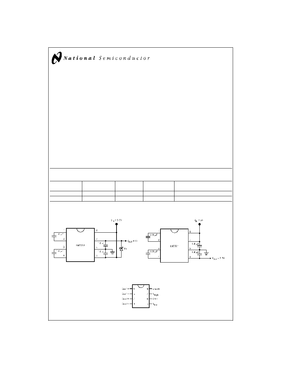
Basic Operating Circuits
Connection Diagram
Step-Up Converter
DS100146-1
Step-Down Converter
DS100146-2
Mini SO8 Package
DS100146-3
Top View
December 1999
LM3351
Switched
Capacitor
V
oltage
Converter
© 1999 National Semiconductor Corporation
DS100146
www.national.com
Absolute Maximum Ratings
(Note 1)
If Military/Aerospace specified devices are required,
please contact the National Semiconductor Sales Office/
Distributors for availability and specifications.
Maximum Input Voltage, Step-Down
5.5V
Maximum Input Voltage, Step-Up
3.65V
Power Dissipation (P
D
) (T
A
=25∞C,
(Note 2))
500 mW
ja
(Note 2)
250∞C/W
Tj Max (Note 2)
150∞C
Storage Temperature
-65∞C to +150∞C
Lead Temperature (Soldering, 10
secs)
260∞C
ESD Susceptibility (Note 3)
2kV
Not short circuit protected.
Operating Conditions
(Note 1)
Ambient Temperature Range
-40∞C to + 85∞C
Electrical Characteristics
3/2 Step-Up Voltage Converter
Specifications in standard type face are for T
j
= 25∞C, and those with boldface type apply over full operating temperature
range. Unless otherwise specified, V
in
= 3.3V, V
Enable
= 3.3V, I
load
= 50 mA, C
1
, C
2
, C
in
and C
out
= 1 µF.
Symbol
Parameter
Conditions
Typ (Note 4)
Limits (Note 5)
Units
V
outNL
Output Voltage at
No Load
I
load
= 0 A
5.0
V
V
outFL
Output Voltage at
50 mA
I
load
= 50 mA
4.7
V
V
in
Input Supply
Voltage Range
3.3
V
2.5
V(Min)
3.65
V(Max)
I
Q1
Quiescent Current
Shutdown Mode, V
Enable
= 0V,
I
load
=0 A; Current into pin V
low
0.025
µA
3
µA(Max)
I
Q2
Quiescent Current
Normal Mode, I
Ioad
= 0A; Current into
pin V
Iow
1.1
mA
1.5
mA(Max)
Z
out
Output Source
Impedance
I
load
= 50 mA
4.2
6.25
(Max)
f
SW
Switching
Frequency
(Note 6)
200
kHz
125
kHz(Min)
275
kHz(Max)
V
Enable
Enable Threshold
Voltage
1.7
V
1.0
V(Min)
2.5
V(Max)
I
Enable
Leakage Current
Current into ENABLE pin; ENABLE =
5V and all other pins at ground
0.025
µA
1
µA(Max)
P
Power Efficiency
95
%
Electrical Characteristics
2/3 Step-Down Voltage Converter
Specifications in standard type face are for T
j
= 25∞C, and those with boldface type apply over full operating temperature
range. Unless otherwise specified, V
high
= 5V, V
Enable
= 5V, I
load
= 50 mA, C
1
, C
2
, C
in
and C
out
= 1 µF.
Symbol
Parameter
Conditions
Typ (Note 4)
Limits (Note 5)
Units
V
outNL
Output Voltage at
No Load
I
load
= 0 A
3.3
V
V
outFL
Output Voltage at
50 mA
I
load
=50 mA
3.2
V
V
in
Input Supply
Voltage Range
5
V
2.2
V(Min)
5.5
V(Max)
I
Q1
Quiescent Current
Shutdown Mode, V
Enable
= 0V,
I
load
=0 A; Current into pin V
high
0.25
µA
3
µA(Max)
LM3351
www.national.com
2
Electrical Characteristics
2/3 Step-Down Voltage Converter
(Continued)
Specifications in standard type face are for T
j
= 25∞C, and those with boldface type apply over full operating temperature
range. Unless otherwise specified, V
high
= 5V, V
Enable
= 5V, I
load
= 50 mA, C
1
, C
2
, C
in
and C
out
= 1 µF.
Symbol
Parameter
Conditions
Typ (Note 4)
Limits (Note 5)
Units
I
Q2
Quiescent Current
Normal Mode, I
Ioad
= 0A; Current into
pin V
high
0.8
mA
1.0
mA(Max)
Z
out
Output Source
Impedance
I
load
= 50 mA
1.8
3
(Max)
f
SW
Switching
Frequency
(Note 6)
200
kHz
125
kHz(Min)
275
kHz(Max)
V
Enable
Enable Threshold
Voltage
1.7
V
1.0
V(Min)
2.5
V(Max)
I
Enable
Leakage Current
Current into ENABLE pin; ENABLE =
5V and all other pins at ground
0.025
µA
1
µA(Max)
P
Power Efficiency
95
%
Note 1: Absolute maximum ratings indicate limits beyond which damage to the device may occur. Operating ratings indicate conditions for which the device is in-
tended to be functional, but do not guarantee specific performance limits. For guaranteed specifications and test conditions, see Electrical Characteristics. The guar-
anteed specifications apply only for the test conditions listed. Some performance characteristics may degrade when the device is not operated under the listed test
conditions.
Note 2: For operation at elevated temperatures, LM3351 must be derated based on package thermal resistance of
ja
and T
j
max, T
j
= T
A
+
ja
P
D
.
Note 3: The human body model is a 100 pF capacitor discharged through a 1.5 kW resistor into each pin.
Note 4: Typical numbers are at 25∞C and represent the most likely parametric norm.
Note 5: Limits are 100% production tested at 25∞C. Limits over the operating temperature range are guaranteed through correlation using Statistical Quality Control
(SQC) methods. The limits are used to calculate National's Averaging Outgoing Quality Level (AOQL).
Note 6: The internal oscillator runs at 1.6 MHz, the output switches operate at one eighth of the oscillator frequency, f
OSC
= 8f
SW
.
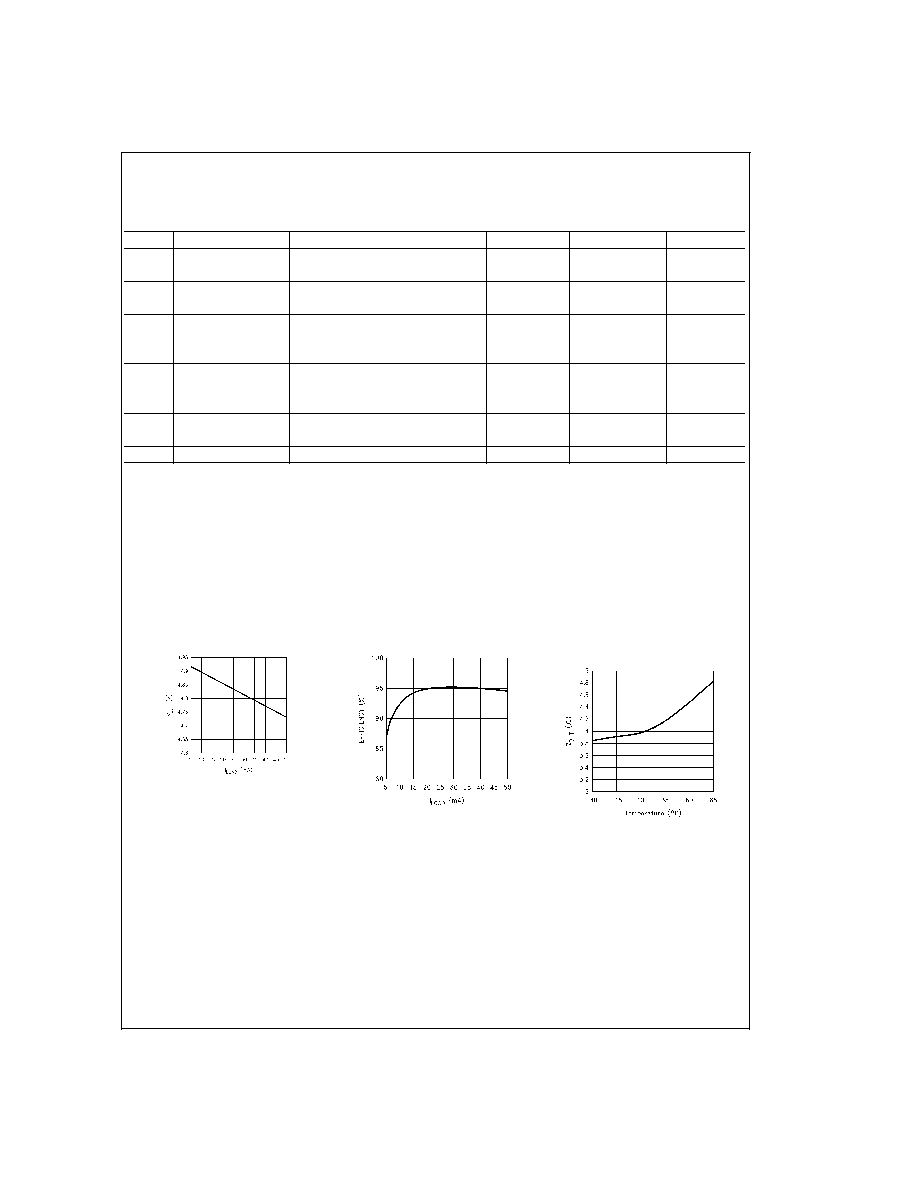
Typical Performance Characteristics
V
out
vs I
load
(Step-Up)
DS100146-4
P
vs I
load
(Step-Up)
DS100146-5
Output Source Impedance vs
Temperature (Step-Up)
DS100146-6
LM3351
www.national.com
3
Typical Performance Characteristics
(Continued)
Pin Description
Pin
Name
Function
1
Cap1+
Positive terminal for the first charge
pump capacitor.
2
Cap1-
Negative terminal for the first charge
pump capacitor.
3
Cap2+
Positive terminal for the second charge
pump capacitor.
4
Cap2-
Negative terminal for the second charge
pump capacitor.
5
V
low
In Step-Up mode, this will be the input
terminal. In Step-Down mode, this will
be the output terminal.
6
Gnd
Ground
7
V
high
In Step-Down mode, this will be the
input terminal. In Step-Up mode, this
will be the output terminal.
8
Enable
Active high CMOS logic level Enable
Input. Connect to Voltage Input terminal
to enable the IC. Connect to Ground
(Pin 6) to disable.
Detailed Operation
OPERATING PRINCIPLE
The LM3351 is a charge-pump voltage converter that pro-
vides a voltage conversion ratio of 3/2 in step-up mode and
a conversion ratio of 2/3 in the step-down mode. Thus it can
be used in the step-down mode to provide a 3.3V output
from a regulated 5V input or in the step-up mode to provide
a 5V output from a regulated 3.3V input. Other values of in-
put voltages can be used as long as they are within the lim-
its.
The LM3351 contains an array of CMOS switches which are
operated in a certain sequence to provide the step-up or
step-down of the input supply. An internal RC oscillator pro-
vides the timing signals.
Energy transfer and storage are provided by four inexpen-
sive ceramic capacitors. The selection of these capacitors is
explained in the Capacitor Selection section under Applica-
tion Information.
V
out
vs I
load
(Step-Down)
DS100146-7
P
vs I
load
(Step-Down)
DS100146-8
Output Source Impedance vs
Temperature (Step-Down)
DS100146-9
Switching Frequency vs
Temperature
DS100146-10
LM3351
www.national.com
4
Detailed Operation
(Continued)
STEP-UP APPLICATIONS NEED AN EXTRA DIODE
The LM3351 is biased from pin V
high
. Thus for step-up appli-
cations, an external Schottky diode (D1) is needed to supply
power to V
high
during startup (See
Figure 1). Note that during
shutdown, this diode will provide a DC path from V
in
to V
out
.
The load may therefore continue to draw current from the in-
put voltage source. This Schottky diode is not required for
step-down applications (See
Figure 2).
SHUTDOWN MODE
When ENABLE is a logic low (ground), the LM3351 enters a
low power shutdown mode. In this mode, all circuitry is dis-
abled and therefore, all switching action stops. During shut-
down, the current consumption drops to 250 nA (typical).
When ENABLE is a logic high, (i.e. 3.3V for step-up mode
and 5.0V for step-down mode), the LM3351 returns to nor-
mal operation.
Application Information
CAPACITOR SELECTION
The LM3351 requires four capacitors: an input bypass ca-
pacitor (connected between V
in
and ground), an output hold
capacitor (connected between V
out
and ground), and two
sampling capacitors (C1 and C2 in
Figures 1, 2). 1.0 µF
(
±
20%) ceramic chip type capacitors are recommended for
all four capacitors. The usable operating frequency should
be greater than 5 MHz for all capacitors.
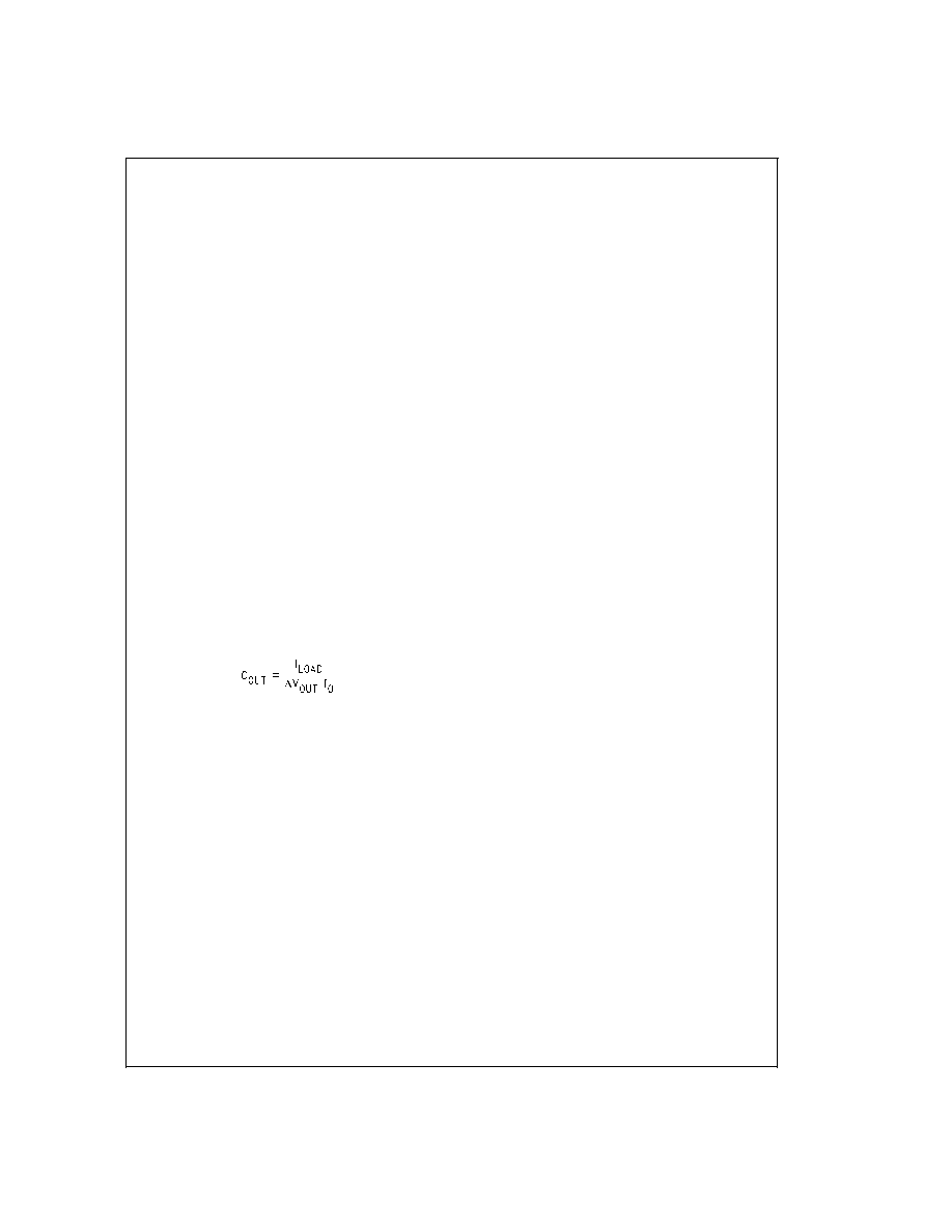
The output hold capacitor value determines the output ripple.
Increasing the value of the hold capacitor decreases the
ripple. The value of this capacitor (C
out
) can be calculated
(approximately) based on the output ripple (
V
out
) require-
ments from:
where I
load
is the load current and f
O
is the oscillator fre-
quency.
In order to ensure superior performance over the entire oper-
ating temperature range, capacitors made of X7R dielectric
material are suggested. However, capacitors made of other
dielectric materials that still meet the
±
20% specification
over the entire temperature range can also be used.
PRECAUTIONS
The LM3351 is not short circuit protected.
LM3351
www.national.com
5