LM3355
Regulated 50mA Buck-Boost Switched Capacitor DC/DC
Converter
General Description
The LM3355 is a CMOS switched capacitor DC/DC con-
verter that produces a regulated output voltage by automati-
cally stepping up (boost) or stepping down (buck) the input
voltage. It accepts an input voltage between 2.5V and 5.5V.
The LM3355 is available with a standard output voltage of
4.1V (ideal for white LED applications). If other output volt-
age options between 1.8V and 4.1V are desired for other
applications, please contact your National Semiconductor
representative.
The LM3355's proprietary buck-boost architecture enables
up to 50 mA of load current at an average efficiency greater
than 75%. Typical operating current is only 375 µA and the
typical shutdown current is only 2.3 µA.
The LM3355 is available in a 10-pin MSOP package. This
package has a maximum height of only 1.1 mm.
The high efficiency of the LM3355, low operating and shut-
down currents, small package size, and the small size of the
overall solution make this device ideal for battery powered,
portable, and hand-held applications.
See the LM3352 for up to 200mA of output current.
Features
n
Regulated V
OUT
with
±
3% accuracy
n
Standard output voltage of 4.1V
n
Custom output voltages available from 1.8V to 4.1V in
100 mV increments
n
2.5V to 5.5V input voltage
n
Up to 50 mA output current
n
>
75% average efficiency
n
Uses few, low-cost external components
n
Very small solution size
n
375 µA typical operating current
n
2.3 µA typical shutdown current
n
1 MHz switching frequency (typical)
n
Architecture and control methods provide high load
current and good efficiency
n
MSOP-10 package
n
Over-temperature protection
Applications
n
White LED display backlights
n
1-cell Lilon battery-operated equipment including PDAs,
hand-held PCs, cellular phones
n
Flat panel displays
n
Hand-held instruments
n
NiCd, NiMH, or alkaline battery powered systems
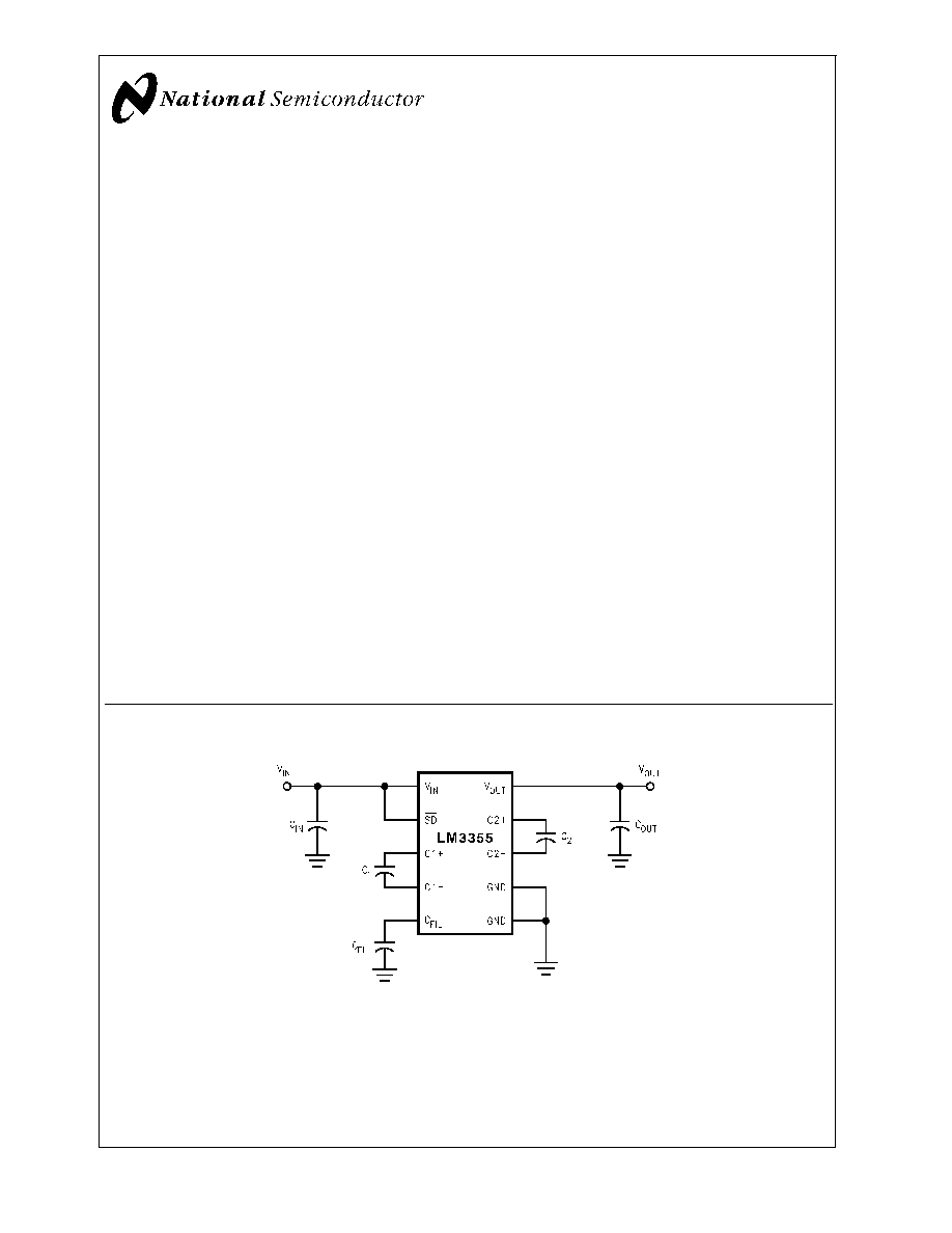
Typical Operating Circuit
DS200219-1
December 2001
LM3355
Regulated
50
mA
Buck-Boost
Switched
Capacitor
DC/DC
Converter
© 2001 National Semiconductor Corporation
DS200219
www.national.com
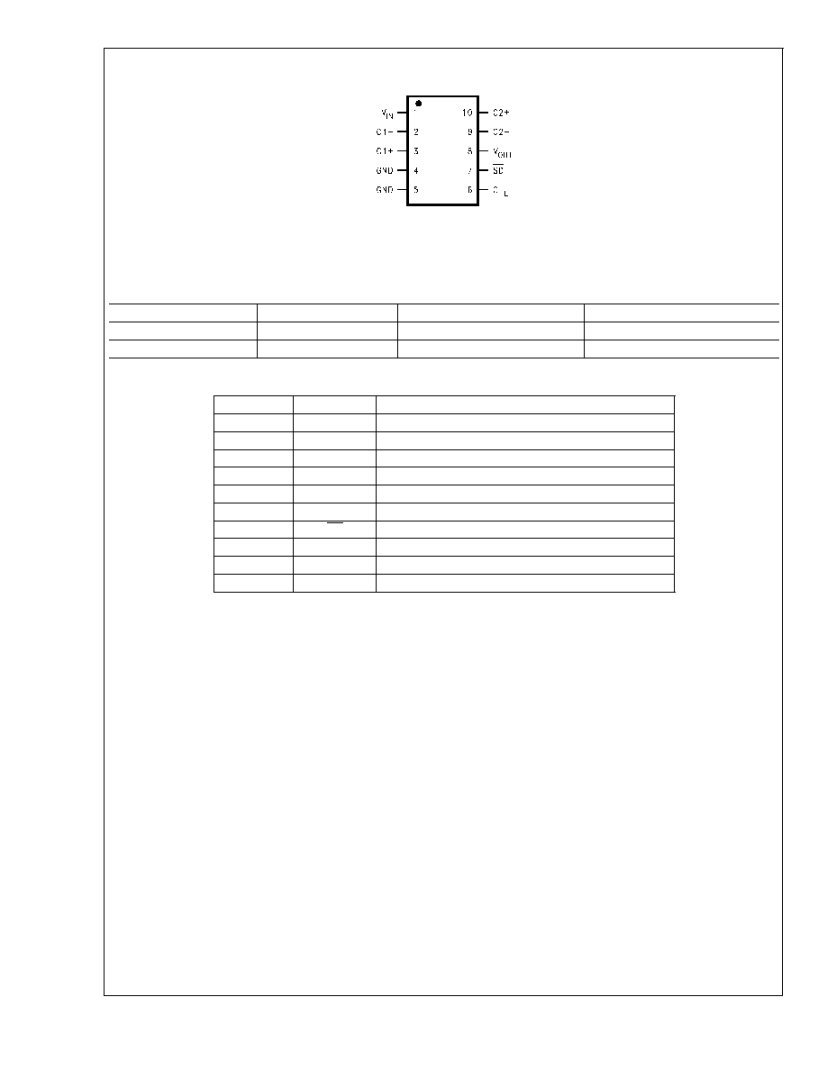
Connection Diagram
Ordering Information
Order Number
Package Type
NSC Package Drawing
Supplied As
LM3355MMX-4.1
MSOP-10
MUB10A
3.5k Units, Tape and Reel
LM3355MM-4.1
MSOP-10
MUB10A
1k Units, Tape and Reel
Pin Description
Pin Number
Name
Function
1
V
IN
Input Supply Voltage
2
C1-
Negative Terminal for C1
3
C1+
Positive Terminal for C1
4
GND
Ground
5
GND
Ground
6
C
FIL
Filter Capacitor, a 1µF capacitor is recommended.
7
SD
Shutdown, active low
8
V
OUT
Regulated Output Voltage
9
C2-
Negative Terminal for C2
10
C2+
Positive Terminal for C2
DS200219-2
Top View
MSOP-10 Pin Package
See NS Package Number MUB10A
LM3355
www.national.com
2

Absolute Maximum Ratings
(Note 1)
If Military/Aerospace specified devices are required,
please contact the National Semiconductor Sales Office/
Distributors for availability and specifications.
All Pins
-0.5V to 5.6V
Power Dissipation (T
A
= 25∞C)
(Note 2)
Internally Limited
T
JMAX
(Note 2)
150∞C
JA
(Note 2)
250∞C/W
Storage Temperature
-65∞C to +150∞C
Lead Temperature (Soldering, 5 sec.)
260∞C
ESD Rating (Note 3)
Human Body Model
Machine Model
1.5 kV
100V
Operating Ratings
Input Voltage (V
IN
)
2.5V to 5.5V
Output Voltage (V
OUT
)
1.8V to 4.1V
Ambient Temperature (T
A
) (Note 2)
-40∞C to +85∞C
Junction Temperature (T
J
) (Note 2)
-40∞C to +125∞C
Electrical Characteristics
Limits in standard typeface are for T
A
= 25∞C, and limits in boldface type apply over the full operating temperature range of
-40∞C
T
A
85∞C. Unless otherwise specified: C
1
= C
2
= 0.33 µF; C
IN
= 10 µF; C
OUT
= 10 µF; C
FIL
= 1 µF; V
IN
= 3.5V.
Parameter
Conditions
Min (Note 5)
Typ (Note 4)
Max (Note 5)
Units
LM3355-4.1
Output Voltage (V
OUT
)
V
IN
= 3.5V; I
LOAD
= 50 mA
4.038
4.1
4.162
V
2.6V
<
V
IN
<
5.5V;
1 mA
<
I
LOAD
<
50 mA
3.977/3.936
4.1
4.223/4.264
2.5V
<
V
IN
<
5.5V;
1 mA
<
I
LOAD
<
40 mA
3.977/3.936
4.1
4.223/4.264
Efficiency
I
LOAD
= 10 mA
80
%
I
LOAD
= 50 mA
75
Output Voltage Ripple
(Peak-to-Peak)
I
LOAD
= 50 mA
C
OUT
= 10 µF ceramic
75
mV
P-P
LM3355-ALL OUTPUT VOLTAGE VERSIONS
Operating Quiescent Current
Measured at Pin V
IN
;
I
LOAD
= 0A (Note 6)
375
475
µA
Shutdown Quiescent Current
SD Pin at 0V (Note 7)
2.3
5
µA
Switching Frequency
0.60
1
1.40
MHz
SD Input Threshold Low
2.5V
<
V
IN
<
5.5V
0.2 V
IN
V
SD Input Threshold High
2.5V
<
V
IN
<
5.5V
0.8 V
IN
V
SD Input Current
Measured at SD Pin;
SD Pin = V
IN
= 5.5V
0.3
µA
Note 1: "Absolute Maximum Ratings" indicate limits beyond which damage to the device may occur. Operating Ratings are conditions for which the device is
intended to be functional, but device parameter specifications may not be guaranteed. For guaranteed specifications and test conditions, see "Electrical
Characteristics".
Note 2: As long as T
A
+85∞C, all electrical characteristics hold true and the junction temperature should remain below +125∞C.
Note 3: The Human Body Model is a 100 pF capacitor discharged through a 1.5 k
resistor into each pin. The Machine Model is a 200 pF capacitor discharged
directly into each pin.
Note 4: Typical numbers are at 25∞C and represent the most likely norm.
Note 5: All limits guaranteed at room temperature (standard typeface) and at temperature extremes (bold typeface). All room temperature limits are 100% tested
or guaranteed through statistical analysis. All limits at temperature extremes are guaranteed by correlation using standard Statistical Quality Control methods (SQC).
All limits are used to calculate Average Outgoing Quality Level (AOQL).
Note 6: The V
OUT
pin is forced to 200 mV above the typical V
OUT
. This is to insure that the internal switches are off.
Note 7: The output capacitor C
OUT
is fully discharged before measurement.
LM3355
www.national.com
3
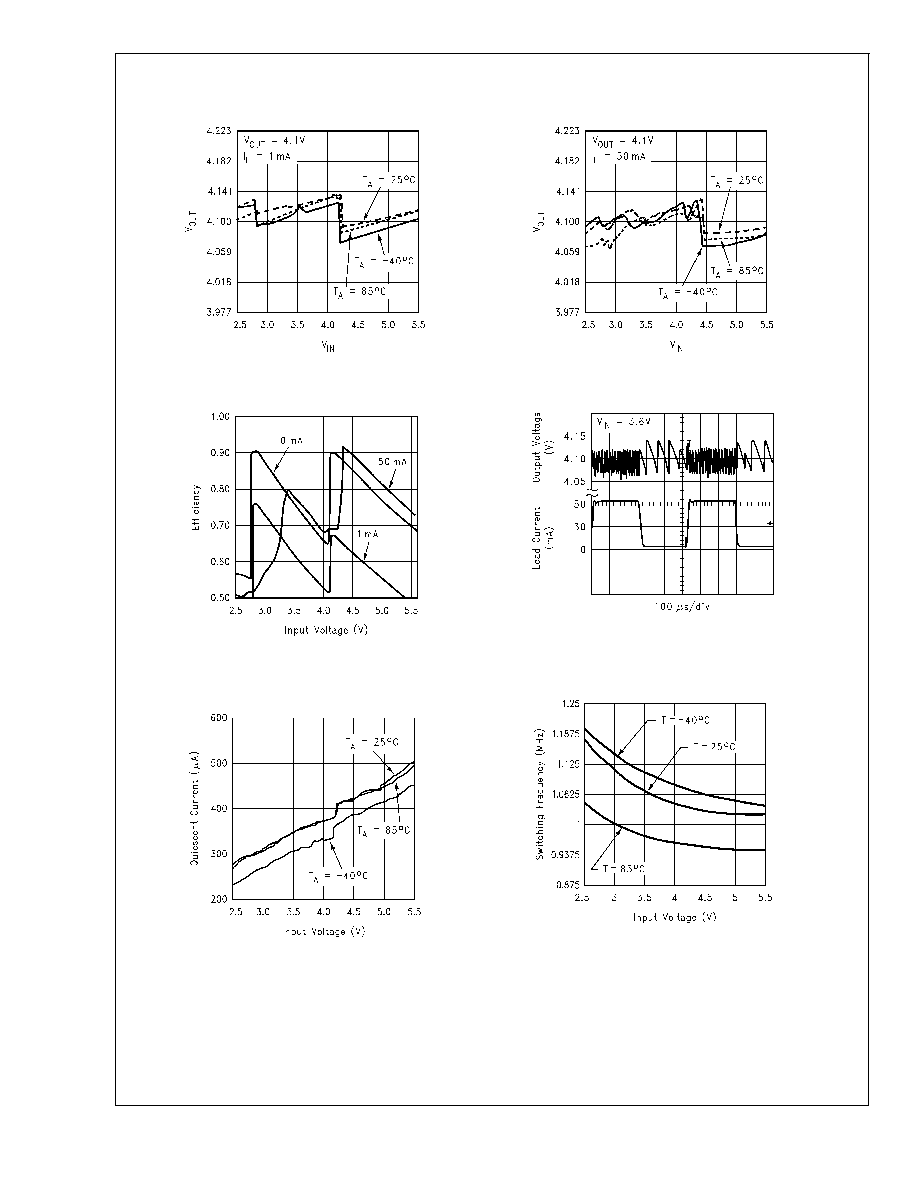
Typical Performance Characteristics
Unless otherwise specified T
A
= 25∞C.
V
OUT
vs. V
IN
DS200219-4
V
OUT
vs. V
IN
DS200219-5
Efficiency vs. V
IN
DS200219-20
Load Transient Response
DS200219-14
Operating Quiescent
Current vs. V
IN
DS200219-24
Switching Frequency vs. V
IN
DS200219-23
LM3355
www.national.com
4
Typical Performance Characteristics
Unless otherwise specified T
A
= 25∞C. (Continued)
Applications Information
Operating Principle
The LM3355 is designed to provide a step-up/step-down
voltage regulation in battery powered systems. It combines
switched capacitor circuitry, reference, comparator, and
shutdown logic in a single 10-pin MSOP package. The
LM3355 can provide a regulated voltage between 1.8V and
4.1V from an input voltage between 2.5V and 5.5V. It can
supply a load current up to 50 mA.
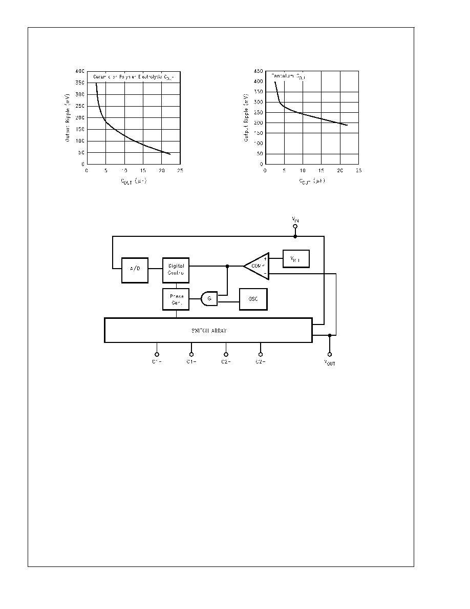
As shown in
Figure 1, the LM3355 employs two feedback
loops to provide regulation in the most efficient manner
possible. The first loop is from V
OUT
through the comparator
COMP, the AND gate G
1
, the phase generator, and the
switch array. The comparator's output is high when V
OUT
is
less than the reference V
REF
. Regulation is provided by
gating the clock to the switch array. In this manner, charge is
transferred to the output only when needed. The second
loop controls the gain configuration of the switch array. This
loop consists of the comparator, the digital control block, the
phase generator, and the switch array. The digital control
block computes the most efficient gain from a set of five
gains based on inputs from the A/D and the comparator. The
gain signal is sent to the phase generator which then sends
the appropriate timing and configuration signals to the switch
array. This dual loop provides regulation over a wide range of
loads efficiently.
Since efficiency is automatically optimized, the curves for
V
OUT
vs. V
IN
and Efficiency vs. V
IN
in the Typical Perfor-
mance Characteristics section exhibit small variations. The
reason is that as input voltage or output load changes, the
digital control loops are making decisions on how to optimize
efficiency. As the switch array is reconfigured, small varia-
tions in output voltage and efficiency result. In all cases
where these small variations are observed, the part is oper-
ating correctly; minimizing output voltage changes and opti-
mizing efficiency.
Charge Pump Capacitor Selection
A 0.33 µF ceramic capacitor is suggested for C1 and C2. To
ensure proper operation over temperature variations, an
X7R dielectric material is recommended.
Maximum V
OUT
Ripple vs. C
OUT
DS200219-32
Maximum V
OUT
Ripple vs. C
OUT
DS200219-30
DS200219-3
FIGURE 1. Block Diagram
LM3355
www.national.com
5