LM3370
Dual Synchronous Step-Down DC-DC Converter with
Dynamic Voltage Scaling Function
General Description
LM3370 is a dual step-down DC-DC converter optimized for
powering ultra-low voltage circuits from a single Li-Ion bat-
tery and input rail ranging from 2.7V to 5.5V. It provides two
outputs with 600mA load per channel. The output voltage
range varies from 1V to 3.3V and can be dynamically con-
trolled using the I
2
C compatible interface. This dynamic volt-
age scaling function allows processors to achieve maximum
performance at the lowest power level. The I
2
C compatible
interface can also be used to control auto PFM-PWM/PWM
mode selection and other performance enhancing features.
The LM3370 offers superior features and performance for
portable systems with complex power management require-
ments. Automatic intelligent switching between PWM low-
noise and PFM low-current mode offers improved system
efficiency. Internal synchronous rectification enhances the
converter efficiency without the use of futher external de-
vices.
There is a power-on-reset function that monitors the level of
the output voltage to avoid unexpected power losses. The
independent enable pin for each output allows for simple and
effective power sequencing.
LM3370 is available in a 4mm by 5mm 16-lead non-pullback
LLP
package.
A
high
switching
frequency -- 2MHz
(typ) -- allows use of tiny surface-mount components includ-
ing a 2.2µH inductor.
Default fixed voltages for the 2 output voltages combination
can be customized to fit system requirements by contacting
National Semiconductor Corporation.
Features
n
I
2
C compatible interface
-- V
OUT1
= 1V to 2V in 50mV steps
-- V
OUT2
= 2.3V to 3.3V in 100mV steps
-- Automatic PFM/PWM mode switching & Forced PWM
mode for low noise operation
-- Spread Spectrum capability using I
2
C
n
600mA load per channel
n
2MHz PWM fixed switching frequency (typ.)
n
Internal synchronous rectification for high efficiency
n
Internal soft start
n
Power-on-reset function for both outputs
n
2.7V
V
IN
5.5V
n
Operates from a single Li-Ion cell or 3 cell NiMH/NiCd
batteries and 3.3V/5.5V fixed rails
n
2.2µH Inductor, 4.7µF Input and 10µF Output Capacitor
per channel
n
16-lead LLP Package (4mm x 5mm x 0.8mm)
Applications
n
Baseband Processors
n
Application Processors (Video, Audio)
n
I/O Power
n
FPGA Power and CPLD
February 2006
LM3370
Dual
Synchronous
Step-Down
DC-DC
Converter
with
Dynamic
V
oltage
Scaling
Function
© 2006 National Semiconductor Corporation
DS201673
www.national.com
Typical Application
Functional Block Diagram
20167301
FIGURE 1. Typical Application Circuit
20167302
FIGURE 2. Functional Diagram
LM3370
www.national.com
2
Package Marking Information
16-Lead LLP Package
20167343
FIGURE 3. Top Marking
20167342
FIGURE 4. Top View
LM3370
www.national.com
3
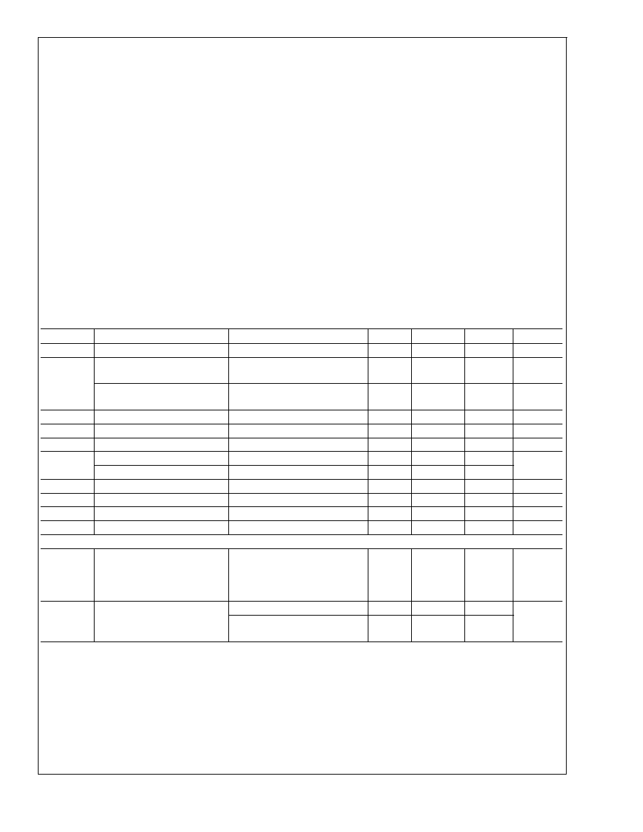
Pin Descriptions
Pin #
Name
Description
1
V
IN2
Power supply voltage input to PFET and NFET switches for Buck 2
2
SW2
Buck 2 Switch Pin
3
PGND2
Buck 2 Power Ground
4
V
DD
Signal supply voltage input, V
DD
must be equal or greater of the two inputs ( V
IN1
&
V
IN2
)
5
SGND
Signal GND
6
PGND1
Buck 1 Power Ground
7
SW1
Buck 1 Switch Pin
8
V
IN1
Power supply voltage input to PFET and NFET switches for Buck 1
9
FB1
Analog Feedback Input for Buck 1
10
SDA
I
2
C Compatible Data, a 2 k
pull up resistor is required.
11
SCL
I
2
C Compatible Clock, a 2 k
pull up resistor is required.
12
nPOR1
Power ON Reset for Buck 1, Open drain output Low when Buck 1 output is 92% of
target output. A 100 k
pull up resistor is required
13
nPOR2
Power ON Reset for Buck 2, Open drain output Low when Buck 2 output is 92% of
target output. A 100 k
pull up resistor is required
14
EN1
Buck 1 Enable
15
EN2
Buck 2 Enable
16
FB2
Analog feedback for Buck 2
I
2
C Controlled Features
Features
Parameter
Comments
Output Voltage
V
OUT1
& V
OUT2
Output voltage is controlled via I
2
C compatible
Modes
Buck 1 & Buck 2
Mode can be controlled via I
2
C
compatible by either forcing device
in Auto mode or forced PWM mode
Spread Spectrum
Buck 1 & Buck 2
Spread Spectrum capability via I
2
C compatible for noise reduction
Ordering Information
Order Number
Voltage Option
Package Marking
Supplied As
LM3370SD-3013*
1.2V & 2.5V
TBD
250 units, Tape-and-Reel
LM3370SDX-3013*
TBD
3000 units, Tape and Reel
LM3370SD-3021
1.2V & 3.3V
S0003TB
250 units, Tape-and-Reel
LM3370SDX-3021
S0003TB
3000 units, Tape-and-Reel
LM3370SD-3416*
1.4V & 2.8V
TBD
250 units, Tape-and-Reel
LM3370SDX-3416*
TBD
3000 units, Tape-and-Reel
LM3370SD-38xx*
1.6V & 1.8V
TBD
250 units, Tape-and-Reel
LM3370SDX-38xx*
TBD
3000 units, Tape-and-Reel
LM3370SD-4221*
1.8V & 3.3V
TBD
250 units, Tape-and-Reel
LM3370SDX-4221*
TBD
3000 units, Tape-and-Reel
Note the LM3370SD-3013 has the following default output voltages where V
OUT1
= 1.2V & V
OUT2
= 2.5V
* Contact National Semiconductor for availability
LM3370
www.national.com
4
Absolute Maximum Ratings
(Notes 1,
2)
If Military/Aerospace specified devices are required,
please contact the National Semiconductor Sales Office/
Distributors for availability and specifications.
V
IN1
, V
IN2
VDD to PGND &
SGND
-0.2V to 6V
PGND to SGND
-0.2V to +0.2V
SDA, SCL, EN, EN2, nPOR1,
nPOR2, SW1, SW2, FB1 &
FB2
(GND - 0.2) to (V
IN
+
0.2V)
Maximum Continuous Power
Dissipation (P
D_MAX
) (Note 3)
Internally Limited
Junction Temperature (T
J-MAX
)
125∞C
Storage Temperature Range
-65∞C to +150∞C
Maximum Lead Temperature
(Soldering)
(Note 4)
ESD Ratings (Note 5)
All Pins
2 kV HBM
200V MM
Operating Ratings
(Notes 1, 2)
Input Voltage Range ((Note 10))
2.7V to 5.5V
Recommended Load Current Per Channel
0mA to 600mA
Junction Temperature (T
J
) Range
-30∞C to +125∞C
Ambient Temperature (T
A
) Range (Note 6)
-30∞C to +85∞C
Thermal Properties
(Note 7)
Junction-to-Ambient Thermal Resistance
(
JA
)
26∞C/W
Electrical Characteristics
(Notes 2, 8, 10)Typical limits appearing in normal type apply for T
J
= 25∞C. Lim-
its appearing in boldface type apply over the entire junction temperature range (T
A
= T
J
= -30∞C to +85∞C). Unless otherwise
noted, V
IN1
= V
IN2
= 3.6V.
Symbol
Parameter
Conditions
Min
Typ
Max
Units
V
FB
Feedback Voltage
(Note 11)
-3.5
+3.5
%
V
OUT
Line Regulation
2.7V
V
IN
5.5V
I
O
= 10mA, V
OUT
= 1.8V
0.031
%/V
Load Regulation
100mA
I
O
600mA
V
IN
= 3.6V, V
OUT
= 1.8V
0.0013
%/mA
I
Q
PFM
Quiescient Current "On"
PFM Mode, Both Bucks ON
34
µA
I
Q
SD
Quiescient Current "Off"
EN1 = EN2 = 0V
0.2
3
µA
I
LIM
Peak Switching Current Limit
V
IN
= 3.6V
850
1200
1400
mA
R
DS_ON
PFET
V
IN
= 3.6V, I
SW
= 200mA
390
500
m
NFET
V
IN
= 3.6V, I
SW
= 200mA
240
350
F
OSC
Internal Oscillator Frequency
1.5
2.0
2.4
MHz
I
EN
Enable (EN) Input Current
0.01
1
µA
V
IL
Enable Logic Low
0.4
V
V
IH
Enable Logic High
1.0
V
POWER ON RESET THRESHOLD/FUNCTION (POR)
nPOR1 &
nPOR2
Delay Time
nPOR1 = Power ON Reset
for Buck 1
50 mS (default)
50
mS
nPOR2 = Power ON Reset
for Buck 2
Can be pre-trimmd to 50 uS, 100
mS & 200 mS
POR
Threshold
Percentage of Target V
OUT
V
OUT
Rising
94
%
V
OUT
Falling, 85% (default), Can
be pre-trimmed to 70% or 94%
85
Note 1: Absolute Maximum Ratings are limits beyond which damage to the device may occur. Operating Ratings are conditions under which operation of the device
is guaranteed. Operating Ratings do not imply guaranteed performance limits. For guaranteed performance limits and associated test conditions, see the Electrical
Characteristics tables.
Note 2: All voltages are with respect to the potential at the GND pin.
Note 3: Internal thermal shutdown circuitry protects the device from permanent damage. The thermal shutdown engages at T
J
= 150∞C (typ.) and disengages at
T
J
= 140∞C(typ.).
Note 4: For detailed soldering specifications and information, please refer to National Semiconductor Application Note 1187: Leadless Leadframe Package (LLP)
(AN-1187).
Note 5: The Human body model is a 100 pF capacitor discharged through a 1.5 k
resistor into each pin. (MIL-STD-883 3015.7) The machine model is a 200 pF
capacitor discharged directly into each pin. (EAIJ)
LM3370
www.national.com
5