LM3411
Precision Secondary Regulator/Driver
General Description
The LM3411 is a low power fixed-voltage (3.3V or 5.0V) pre-
cision shunt regulator designed specifically for driving an op-
toisolator to provide feedback isolation in a switching regula-
tor.
The LM3411 circuitry includes an internally compensated op
amp, a bandgap reference, NPN output transistor, and volt-
age setting resistors.
A trimmed precision bandgap reference with temperature
drift curvature correction, provides a guaranteed 1% preci-
sion over the operating temperature range (A grade version).
The amplifier's inverting input is externally accessible for
loop frequency compensation when used as part of a larger
servo system. The output is an open-emitter NPN transistor
capable of driving up to 15 mA of load current.
Because of its small die size, the LM3411 has been made
available in the sub-miniature 5-lead SOT23-5 surface
mount package. This package is ideal for use in space criti-
cal applications.
Although its main application is to provide a precision output
voltage (no trimming required) and maintain very good regu-
lation in isolated DC/DC converters, it can also be used with
other types of voltage regulators or power semiconductors to
provide a precision output voltage without precision resistors
or trimming.
Features
n
Fixed voltages of 3.3V and 5.0V with initial tolerance of
Ī
1% for standard grade and
Ī
0.5% for A grade
n
Custom voltages available (3V≠17V)
n
Wide output current range, 20 ĶA≠15 mA
n
Low temperature coefficient
n
Available in 5-lead SOT23-5 surface mount package
(tape and reel)
Applications
n
Secondary controller for isolated DC/DC PWM switching
regulators systems
n
Use with LDO regulator for high-precision fixed output
regulators
n
Precision monitoring applications
n
Use with many types of regulators to increase precision
and improve performance
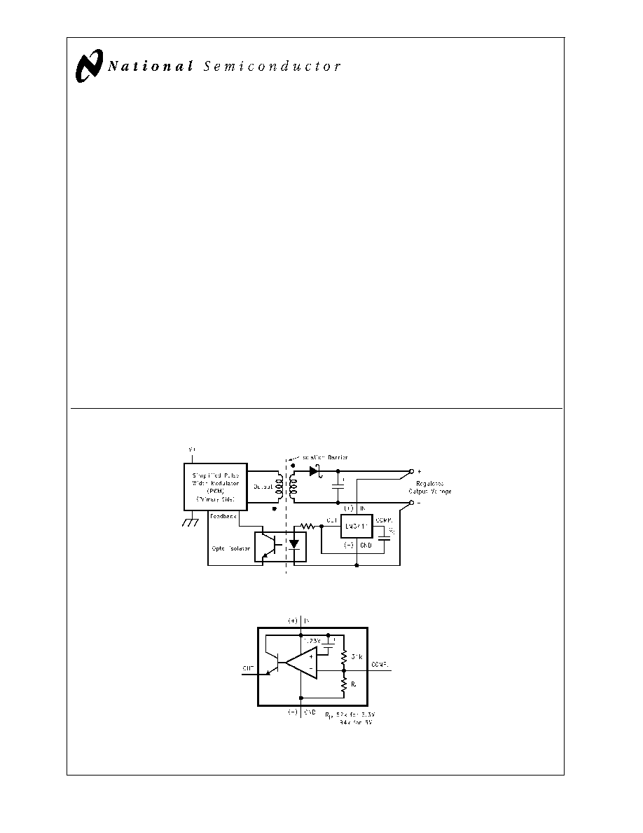
Typical Application and Functional Diagram
SIMPLE SWITCHER
TM
is a tradmark of National Semiconductor Corporation.
DS011987-1
Basic Isolated DC/DC Converter
DS011987-2
LM3411 Functional Diagram
July 2000
LM341
1
Precision
Secondary
Regulator/Driver
© 2000 National Semiconductor Corporation
DS011987
www.national.com
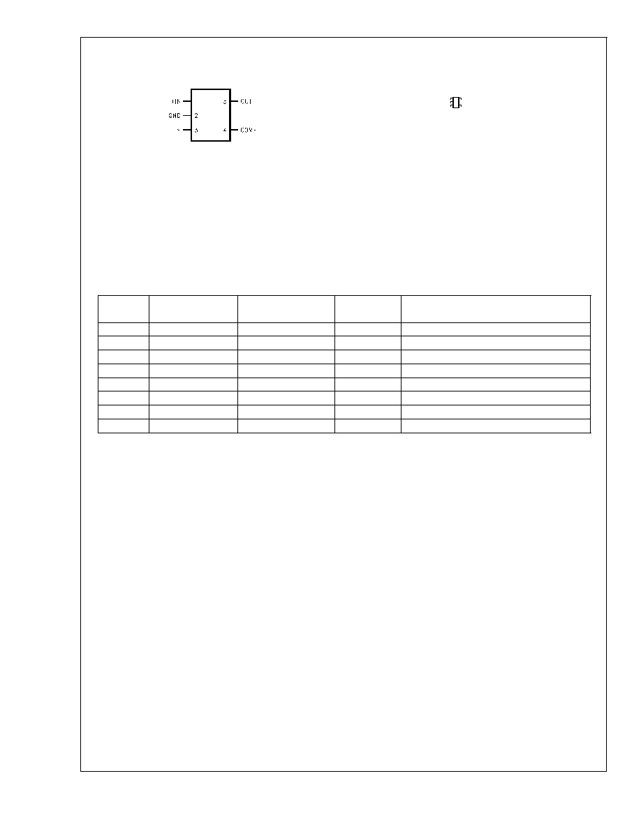
Connection Diagrams and Order Information
Five Lead Surface Mount Package Marking
and Order Information (SOT23-5)
The small SOT23-5 package allows only 4 alphanumeric characters to identify the product. The table below contains the field in-
formation marked on the package.
The first letter "D" identifies the part as a Driver, the next two numbers indicate the voltage, "00" for 3.3V part and "01" for a 5V
part. The fourth letter indicates the grade, "B" for standard grade, "A" for the prime grade.
The SOT23-5 surface mount package is only available on tape in quantities increments of 250 on tape and reel (indicated by the
letters "M5" in the part number), or in quantities increments of 3000 on tape and reel (indicated by the letters "M5X" in the part
number).
5-Lead Small Outline Package (M5)
DS011987-3
*No internal connection, but should be soldered to PC board for best heat
transfer.
Top View
Actual Size
DS011987-4
For Ordering Information
See
Figure 1 in this Data Sheet
See NS Package Number MF05A
Grade
Order Information
Package
Marking
Supplied as
3.3V
A (Prime)
LM3411AM5-3.3
D00A
1000 unit increments on tape and reel
3.3V
A (Prime)
LM3411AM5X-3.3
D00A
3000 unit increments on tape and reel
3.3V
B (Standard)
LM3411M5-3.3
D00B
1000 unit increments on tape and reel
3.3V
B (Standard)
LM3411M5X-3.3
D00B
3000 unit increments on tape and reel
5.0V
A (Prime)
LM3411AM5-5.0
D01A
1000 unit increments on tape and reel
5.0V
A (Prime)
LM3411AM5X-5.0
D01A
3000 unit increments on tape and reel
5.0V
B (Standard)
LM3411M5-5.0
D01B
1000 unit increments on tape and reel
5.0V
B (Standard)
LM3411M5X-5.0
D01B
3000 unit increments on tape and reel
FIGURE 1. SOT23-5 Marking and Order Information
LM341
1
www.national.com
2
Absolute Maximum Ratings
(Note 1)
If Military/Aerospace specified devices are required,
please contact the National Semiconductor Sales Office/
Distributors for availability and specifications.
Input Voltage V(IN)
20V
Output Current
20 mA
Junction Temperature
150įC
Storage Temperature
-65įC to +150įC
Lead Temperature
Vapor Phase (60 sec.)
+215įC
Infrared (15 sec.)
+220įC
Power Dissipation (T
A
= 25įC) (Note
2)
300 mW
ESD Susceptibility (Note 3)
Human Body Model
1500V
See AN-450 "Surface Mounting Methods and Their Effect on
Product Reliability" for methods on soldering surface-mount
devices.
Operating Ratings
(Notes 1, 2)
Ambient Temperature Range
-40įC
T
A
+85įC
Junction Temperature Range
-40įC
T
J
+125įC
Output Current
15 mA
LM3411-3.3 Electrical Characteristics
Specifications with standard type face are for T
J
= 25įC, and those with boldface type apply over full Operating Tempera-
ture Range. Unless otherwise specified, V(IN) = V
REG
, V
OUT
= 1.5V.
Symbol
Parameter
Conditions
Typical
LM3411A-3.3
LM3411-3.3
Units
(Note 4)
Limit
Limit
(Limits)
(Note 5)
(Note 5)
V
REG
Regulation Voltage
I
OUT
= 5 mA
3.3
V
3.317/3.333
3.333/3.366
V(max)
3.284/3.267
3.267/3.234
V(min)
Regulation Voltage
I
OUT
= 5 mA
Ī
0.5/
Ī
1
Ī
1/
Ī
2
%(max)
Tolerance
I
q
Quiescent Current
I
OUT
= 5 mA
85
ĶA
110/115
125/150
ĶA(max)
G
m
Transconductance
20 ĶA
I
OUT
1 mA
3.3
mA/mV
I
OUT
/
V
REG
1.5/0.75
1/0.50
mA/mV(min)
1 mA
I
OUT
15 mA
6.0
mA/mV
3.3/2.0
2.5/1.7
mA/mV(min)
A
V
Voltage Gain
1V
V
OUT
V
REG
- 1.2V (-1.3)
1000
V/V
V
OUT
/
V
REG
R
L
= 140
(Note 6)
550/250
450/200
V/V(min)
1V
V
OUT
V
REG
- 1.2V (-1.3)
3500
V/V
R
L
= 2 k
1500/900
1000/700
V/V(min)
V
SAT
Output Saturation
V(IN) = V
REG
+100 mV
1.0
V
(Note 7)
I
OUT
= 15 mA
1.2/1.3
1.2/1.3
V(max)
I
L
Output Leakage
V(IN) = V
REG
-100 mV
0.1
ĶA
Current
V
OUT
= 0V
0.5/1.0
0.5/1.0
ĶA(max)
R
f
Internal Feedback
52
k
Resistor (Note 8)
65
65
k
(max)
39
39
k
(min)
E
n
Output Noise
I
OUT
= 1 mA, 10 Hz
f
10 kHz
50
ĶV
RMS
Voltage
LM341
1
www.national.com
3

LM3411-5.0 Electrical Characteristics
Specifications with standard type face are for T
J
= 25įC, and those with boldface type apply over full Operating Tempera-
ture Range. Unless otherwise specified, V(IN) = V
REG
, V
OUT
= 1.5V.
Symbol
Parameter
Conditions
Typical
LM3411A-5.0
LM3411-5.0
Units
(Note 4)
Limit
Limit
(Limits)
(Note 5)
(Note 5)
V
REG
Regulation Voltage
I
OUT
= 5 mA
5
V
5.025/5.050
5.050/5.100
V(max)
4.975/4.950
4.950/4.900
V(min)
Regulation Voltage
I
OUT
= 5 mA
Ī
0.5/
Ī
1
Ī
1/
Ī
2
%(max)
Tolerance
I
q
Quiescent Current
I
OUT
= 5 mA
85
ĶA
110/115
125/150
ĶA(max)
G
m
Transconductance
20 ĶA
I
OUT
1 mA
3.3
mA/mV
I
OUT
/
V
REG
1.5/0.75
1.0/0.5
mA/mV(min)
1 mA
I
OUT
15 mA
6.0
mA/mV
3.3/2.0
2.5/1.7
mA/mV(min)
A
V
Voltage Gain
1V
V
OUT
V
REG
- 1.2V (-1.3)
1000
V/V
V
OUT
/
V
REG
R
L
= 250
(Note 6)
750/350
650/300
V/V(min)
1V
V
OUT
V
REG
- 1.2V (-1.3)
3500
V/V
R
L
= 2 k
1500/900
1000/700
V/V(min)
V
SAT
Output Saturation
V(IN) = V
REG
+100 mV
1.0
V
(Note 7)
I
OUT
= 15 mA
1.2/1.3
1.2/1.3
V(max)
I
L
Output Leakage
V(IN) = V
REG
-100 mV
0.1
ĶA
Current
V
OUT
= 0V
0.5/1.0
0.5/1.0
ĶA(max)
R
f
Internal Feedback
94
k
Resistor (Note 8)
118
118
k
(max)
70
70
k
(min)
E
n
Output Noise
I
OUT
= 1 mA, 10 Hz
f
10 kHz
80
ĶV
RMS
Voltage
Note 1: Absolute Maximum Ratings indicate limits beyond which damage to the device may occur. Operating Ratings indicate conditions for which the device is in-
tended to be functional, but do not guarantee specific performance limits. For guaranteed specifications and test conditions, see the Electrical Characteristics. The
guaranteed specifications apply only for the test conditions listed. Some performance characteristics may degrade when the device is not operated under the listed
test conditions.
Note 2: The maximum power dissipation must be derated at elevated temperatures and is dictated by T
Jmax
(maximum junction temperature),
JA
(junction to am-
bient thermal resistance), and T
A
(ambient temperature). The maximum allowable power dissipation at any temperature is (P
Dmax
= T
Jmax
- T
A
)/
JA
or the number
given in the Absolute Maximum Ratings, whichever is lower. The typical thermal resistance (
JA
) when soldered to a printed circuit board is approximately 306įC/W
for the M5 package.
Note 3: The human body model is a 100 pF capacitor discharged through a 1.5 k
resistor into each pin.
Note 4: Typical numbers are at 25įC and represent the most likely parametric norm.
Note 5: Limits are 100% production tested at 25įC. Limits over the operating temperature range are guaranteed through correlation using Statistical Quality Control
(SQC) methods. The limits are used to calculate National's Averaging Outgoing Level (AOQL).
Note 6: Actual test is done using equivalent current sink instead of a resistor load.
Note 7: V
SAT
= V(IN) - V
OUT
, when the voltage at the IN pin is forced 100 mV above the nominal regulating voltage (V
REG
).
Note 8: See Applications and Curves sections for information on this resistor.
LM341
1
www.national.com
4
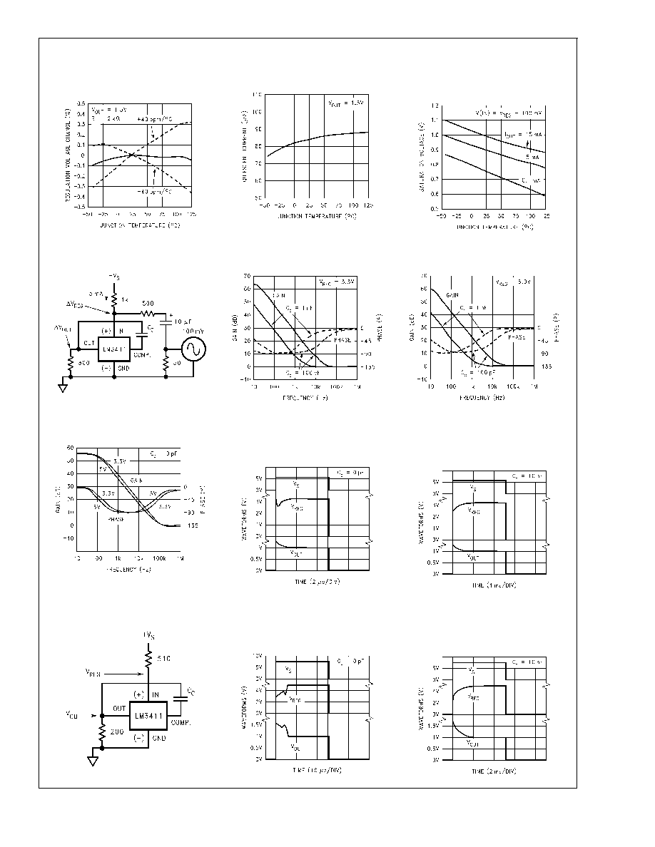
Typical Performance Characteristics
Normalized
Temperature Drift
DS011987-30
Quiescent Current
DS011987-31
Output Saturation
Voltage (V)
SAT
DS011987-32
Circuit Used for Bode Plots
DS011987-8
Bode Plot
DS011987-33
Bode Plot
DS011987-34
Bold Plot
DS011987-44
Response Time
for 3.3V Version
(C
C
= 0 pF)
DS011987-35
Response Time
for 3.3V Version
(C
C
= 10 nF)
DS011987-36
Circuit Used for Response Time
DS011987-11
Response Time
for 5V Version
(C
C
= 0 pF)
DS011987-37
Response Time
for 5V Version
(C
C
= 10 nF)
DS011987-38
LM341
1
www.national.com
5

Typical Performance Characteristics
(Continued)
Tempco of Internal
Feedback Resistor (Rf)
DS011987-39
Regulation Voltage
Change vs
Output Current
DS011987-40
Regulation Voltage vs
Output Voltage and
Load Resistance
DS011987-41
Regulation Voltage vs
Output Voltage and
Load Resistance
DS011987-42
LM341
1
www.national.com
6

Product Description
The LM3411 is a shunt regulator specifically designed to be
the reference and control section in an overall feedback loop
of a regulated power supply. The regulated output voltage is
sensed between the IN pin and GROUND pin of the LM3411.
If the voltage at the IN pin is less than the LM3411 regulating
voltage (V
REG
), the OUT pin sources no current. As the volt-
age at the IN pin approaches the V
REG
voltage, the OUT pin
begins sourcing current. This current is then used to drive a
feedback device, (opto-coupler) or a power device, (linear
regulator, switching regulator, etc.) which servos the output
voltage to be the same value as V
REG
.
In some applications, (even under normal operating condi-
tions) the voltage on the IN pin can be forced above the
V
REG
voltage. In these instances, the maximum voltage ap-
plied to the IN pin should not exceed 20V. In addition, an ex-
ternal resistor may be required on the OUT pin to limit the
maximum current to 20 mA.
Compensation
The inverting input of the error amplifier is brought out to al-
low overall closed-loop compensation. In many of the appli-
cations circuits shown here, compensation is provided by a
single capacitor connected from the compensation pin to the
out pin of the LM3411. The capacitor values shown in the
schematics are adequate under most conditions, but they
can be increased or decreased depending on the desired
loop response. Applying a load pulse to the output of a regu-
lator circuit and observing the resultant output voltage re-
sponse is a easy method of determining the stability of the
control loop. Analyzing more complex feedback loops re-
quires additional information.
The formula for AC gain at a frequency (f) is as follows;
where R
f
52 k
for the 3.3V part, and R
f
94 k
for the 5V
part.
The resistor (R
f
) in the formula is an internal resistor located
on the die. Since this resistor value will affect the phase mar-
gin, the worst case maximum and minimum values are im-
portant when analyzing closed loop stability. The minimum
and maximum room temperature values of this resistor are
specified in the Electrical Characteristics section of this data
sheet, and a curve showing the temperature coefficient is
shown in the curves section. In the applications shown here,
the worst case phase margin occurs with minimum values of
R
f
.
Test Circuit
The test circuit shown in
Figure 2 can be used to measure
and verify various LM3411 parameters. Test conditions are
set by forcing the appropriate voltage at the V
OUT
Set test
point and selecting the appropriate R
L
or I
OUT
as specified in
the Electrical Characteristics section. Use a DVM at the
"measure" test points to read the data.
DS011987-14
FIGURE 2. LM3411 Test Circuit
LM341
1
www.national.com
7
Applications Information
The LM3411 regulator/driver provides the reference and
feedback drive functions in a regulated power supply. It can
also be used together with many different types of regula-
tors, (both linear and switching) as well as other power semi-
conductor devices to add precision and improve regulation
specifications. Output voltage tolerances better than 0.5%
are possible without using trim pots or precision resistors.
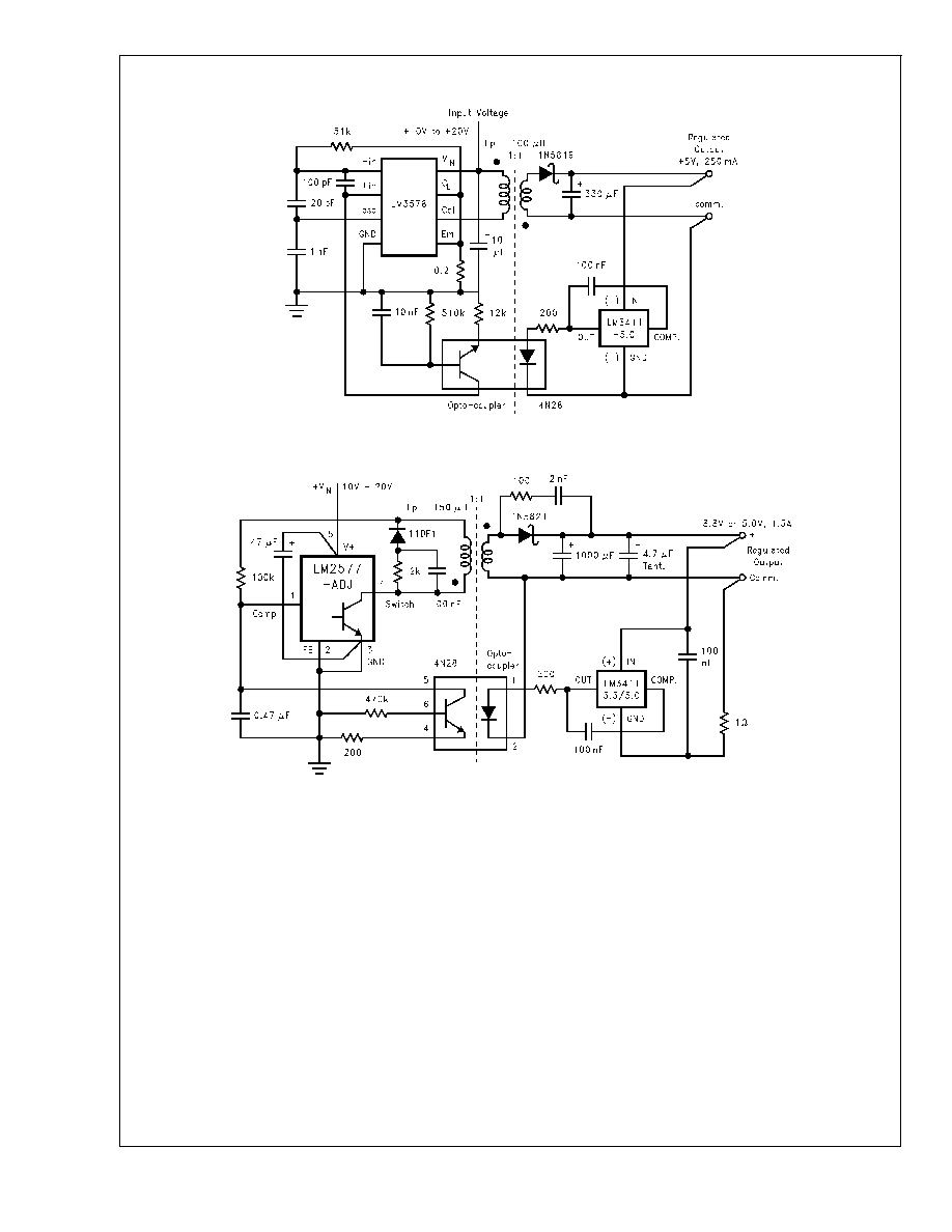
One of the main applications of the LM3411 is to drive an
opto-isolator to provide feedback signal isolation in a switch-
ing regulator circuit. For low current applications, (up to 250
mA) the circuit shown in
Figure 3 provides good regulation
and complete input/output electrical isolation.
For an input voltage of 15V, this circuit can provide an output
of either 3.3V or 5V with a load current up to 250 mA with ex-
cellent regulation characteristics. With the part values
shown, this circuit operates at 80 kHz., and can be synchro-
nized to a clock or an additional LM3578. (See LM1578 data
sheet for additional information.)
An isolated DC/DC flyback converter capable of higher out-
put current is shown in
Figure 4. This circuit utilizes the
LM2577 SIMPLE SWITCHER
TM
voltage regulator for the
Pulse Width Modulation (PWM), power switch and protection
functions, while the LM3411 provides the voltage reference,
gain and opto coupler drive functions. In this circuit, the ref-
erence and error amplifier in the LM2577 are not used (note
that the feedback pin is grounded). The gain is provided by
the LM3411. Since the voltage reference is located on the
secondary side of the transformer, this circuit provides very
good regulation specifications.
The output of a switching regulator typically will contain a
small ripple voltage at the switching frequency and may also
contain voltage transients. These transient voltage spikes
can be sensed by the LM3411 and could give an incorrect
regulation voltage. An RC filter consisting of a 1
resistor
and a 100 nF capacitor will filter these transients and mini-
mize this problem. The 1
resistor should be located on the
ground side of the LM3411, and the capacitor should be
physically located near the package.
DS011987-15
FIGURE 3. Isolated 250 mA Flyback Switching Regulator
DS011987-16
FIGURE 4. Isolated 1.5A Flyback Switching Regulator Using a LM2577
LM341
1
www.national.com
8

Applications Information
(Continued)
Improved output voltage tolerance and regulation specifica-
tions are possible by combining the LM3411A with one of the
SIMPLE SWITCHER buck regulator IC's, such as the
LM2574, LM2575, or LM2576. The circuit shown in
Figure 5
can provide a 5V,
Ī
0.5% Output (1% over the operating tem-
perature range) without using any trim-pots or precision re-
sistors. Typical line regulation numbers are a 1 mV change
on the output for a 8V≠18V change on the input, and load
regulation of 1 mV with a load change from 100 mA≠1A.
A DC-DC flyback converter that accepts a negative input
voltage, and delivers either a positive or negative output is
shown in
Figure 6. The circuit utilizes a buck regulator (such
as the LM2574, LM2575, or LM2576, depending on how
much output current is needed) operating in a flyback con-
figuration. The LM3411 provides the reference and the re-
quired level shifting circuitry needed to make the circuit work
correctly.
A unique feature of this circuit is the ability to ground either
the high or low side of the output, thus generating either a
negative or a positive output voltage. Although no isolation is
provided, with the addition of an opto-isolator and related
components, this circuit could provide input/output isolation.
Combining a LM3411A-5.0 with a 1A low dropout linear regu-
lator results in a 5V
Ī
0.5% (1% over the operating tempera-
ture range) regulator with excellent regulation specifications,
with no trimming or 1% resistors needed.
An added benefit of this circuit (and also true of many of the
other circuits shown here) is the high-side and low-side re-
mote output voltage sensing feature. Sensing the output
voltage at the load eliminates the voltage drops associated
with wire resistance, thus providing near perfect load regula-
tion.
A 5V, 1A regulator circuit featuring low dropout, very good
regulation specifications, self protection features and allows
output voltage sensing is shown in
Figure 7. The regulator
used is a LM2941 adjustable low dropout positive regulator,
which also features an ON/OFF pin to provide a shutdown
feature.
DS011987-17
FIGURE 5. Precision 1A Buck Regulator
DS011987-18
FIGURE 6. Negative Input, Negative or Positive Output Flyback Regulator
LM341
1
www.national.com
9

Applications Information
(Continued)
The circuit in
Figure 8 shows a 3.3V low dropout regulator
using the LM3411-3.3 and several discrete components.
This circuit is capable of excellent performance with both the
dropout voltage and the ground pin current specifications im-
proved over the LM2941/LM3411 circuit.
The standard LM317 three terminal adjustable regulator cir-
cuit can greatly benefit by adding a LM3411. Performance is
increased and features are added. The circuit shown in
Fig-
ure 9 provides much improved line and load regulation,
lower temperature drift, and full remote output voltage sens-
ing on both the high and low side. In addition, a precise cur-
rent limit or constant current feature is simple to add.
Current limit protection in most IC regulators is mainly to pro-
tect the IC from gross over-current conditions which could
otherwise fuse bonding wires or blow IC metalization, there-
fore not much precision is needed for the actual current limit
values. Current limit tolerances can sometimes vary from
Ī
10% to as high as +300% over manufacturing and tem-
perature variations. Often critical circuitry requires a much
tighter control over the amount of current the power supply
can deliver. For example, a power supply may be needed
that can deliver 100% of its design current, but can still limit
the maximum current to 110% to protect critical circuitry from
high current fault conditions.
The circuit in
Figure 9 can provide a current limit accuracy
that is better than
Ī
4%, over all possible variations, in addi-
tion to having excellent line, load and temperature
specifications.
Like the positive regulators, the performance of negative ad-
justable regulators can also be improved by adding the
LM3411. Output voltages of either 3.3V or 5V at currents up
to 1.5A (3A when using a LM333) are possible. Adding two
resistors to the circuit in
Figure 10 adds the precision current
limit feature as shown in
Figure 11. Current limit tolerances
of
Ī
4% over manufacturing and temperature variations are
possible with this circuit.
DS011987-19
FIGURE 7. Precision 5V 1A Low Dropout Regulator
DS011987-20
FIGURE 8. 3.3V 0.5A Low Dropout Regulator
DS011987-21
FIGURE 9. Precision Positive Voltage Regulator with Accurate Current Limit
LM341
1
www.national.com
10

Applications Information
(Continued)
A simple 5V supply monitor circuit is shown in
Figure 12. Us-
ing the LM3411's voltage reference, op-amp (as a compara-
tor) and output driver, this circuit provides a LED indication of
the presence of the 5V supply.
The LM3411 initial room temperature tolerance is
Ī
1% and
Ī
0.5% for the "A" grade part. If a tighter tolerance is needed,
a trim scheme is shown in
Figure 13 that provides approxi-
mately
Ī
1% adjustment range of the regulation voltage
(V
REG
).
The LM3411 is guaranteed to drive a 15 mA load, but if more
current is needed, a NPN boost transistor can be added. The
circuit shown in
Figure 14 is a shunt regulator capable of pro-
viding excellent regulation over a very wide range of current.
Perhaps one of the simplest applications for the LM3411 is
the voltage detector circuit shown in
Figure 15 . The OUT pin
is low when the input voltage is less than V
REG
. When the
V(IN) pin rises above V
REG
, the OUT pin is pulled high by the
internal NPN output resistor.
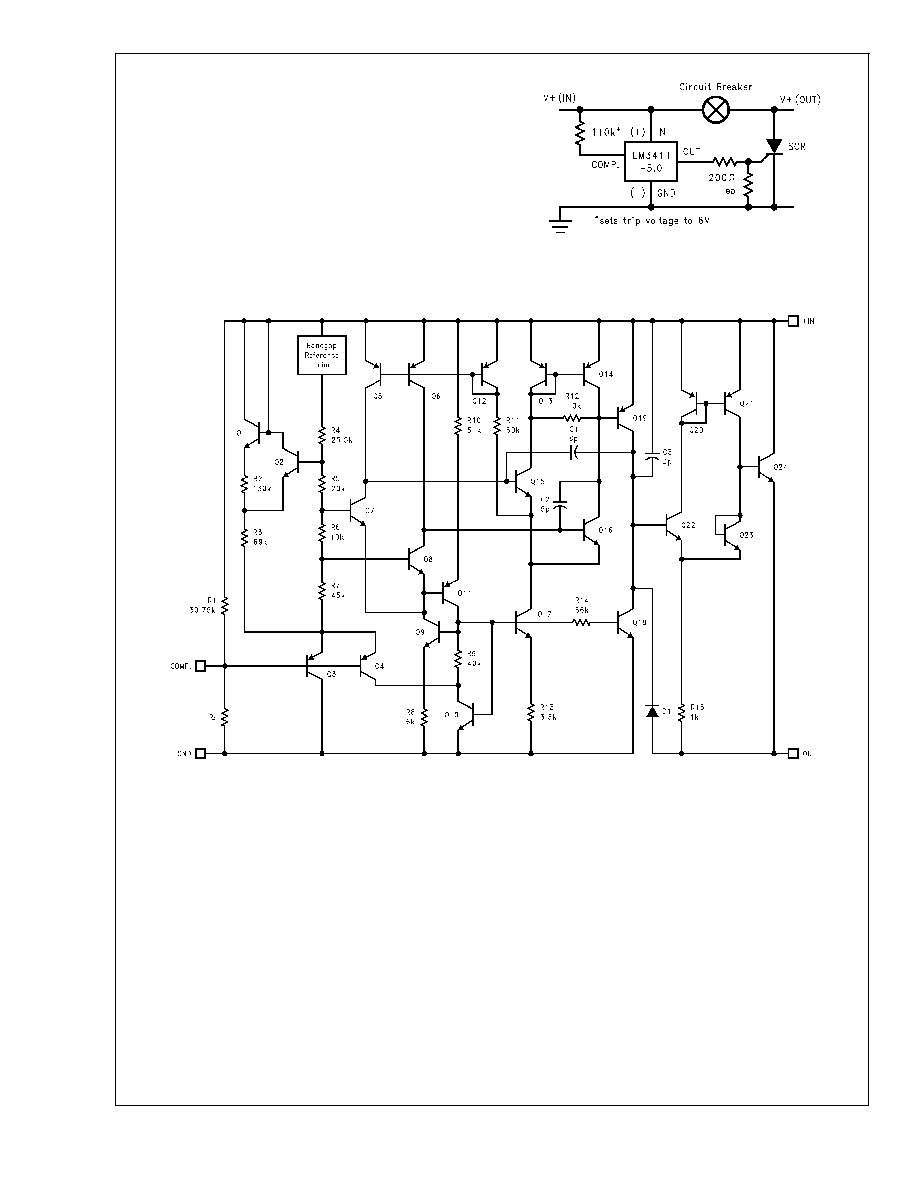
Also an overvoltage detector, the crowbar circuit shown in
Figure 16 is normally located at the output of a power supply
to protect the load from an overvoltage condition should the
power supply fail with an input/output short.
DS011987-22
FIGURE 10. Precision Negative Voltage Regulator
DS011987-23
FIGURE 11. Precision Negative Voltage
Regulator with Accurate Current Limit
DS011987-24
FIGURE 12. 4.7V Power ON Detector with Hysteresis
DS011987-25
FIGURE 13.
Ī
50 mV External Trim
DS011987-26
FIGURE 14. 250 mA Shunt Regulator
DS011987-27
FIGURE 15. Voltage Detector
LM341
1
www.national.com
11
Applications Information
(Continued)
Schematic Diagram
DS011987-28
FIGURE 16. Overvoltage Crowbar
DS011987-29
LM341
1
www.national.com
12
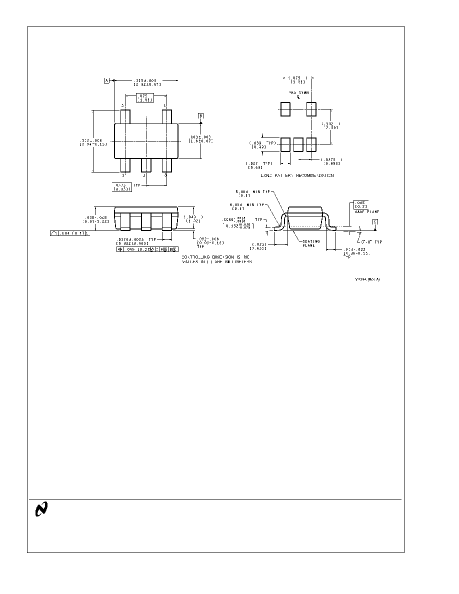
Physical Dimensions
inches (millimeters) unless otherwise noted
LIFE SUPPORT POLICY
NATIONAL'S PRODUCTS ARE NOT AUTHORIZED FOR USE AS CRITICAL COMPONENTS IN LIFE SUPPORT
DEVICES OR SYSTEMS WITHOUT THE EXPRESS WRITTEN APPROVAL OF THE PRESIDENT AND GENERAL
COUNSEL OF NATIONAL SEMICONDUCTOR CORPORATION. As used herein:
1. Life support devices or systems are devices or
systems which, (a) are intended for surgical implant
into the body, or (b) support or sustain life, and
whose failure to perform when properly used in
accordance with instructions for use provided in the
labeling, can be reasonably expected to result in a
significant injury to the user.
2. A critical component is any component of a life
support device or system whose failure to perform
can be reasonably expected to cause the failure of
the life support device or system, or to affect its
safety or effectiveness.
National Semiconductor
Corporation
Americas
Tel: 1-800-272-9959
Fax: 1-800-737-7018
Email: support@nsc.com
National Semiconductor
Europe
Fax: +49 (0) 180-530 85 86
Email: europe.support@nsc.com
Deutsch Tel: +49 (0) 69 9508 6208
English
Tel: +44 (0) 870 24 0 2171
FranÁais Tel: +33 (0) 1 41 91 8790
National Semiconductor
Asia Pacific Customer
Response Group
Tel: 65-2544466
Fax: 65-2504466
Email: ap.support@nsc.com
National Semiconductor
Japan Ltd.
Tel: 81-3-5639-7560
Fax: 81-3-5639-7507
www.national.com
5-Lead Small Outline Package (M5)
Order Number LM3411M5-3.3, LM3411AM5-3.3,
LM3411M5-5.0 or LM3411AM5-5.0
NS Package Number MF05A
LM341
1
Precision
Secondary
Regulator/Driver
National does not assume any responsibility for use of any circuitry described, no circuit patent licenses are implied and National reserves the right at any time without notice to change said circuitry and specifications.