LM3411
Precision Secondary Regulator/Driver
General Description
The LM3411 is a low power fixed-voltage (3.3V or 5.0V) pre-
cision shunt regulator designed specifically for driving an op-
toisolator to provide feedback isolation in a switching regula-
tor.
The LM3411 circuitry includes an internally compensated op
amp, a bandgap reference, NPN output transistor, and volt-
age setting resistors.
A trimmed precision bandgap reference with temperature
drift curvature correction, provides a guaranteed 1% preci-
sion over the operating temperature range (A grade version).
The amplifier's inverting input is externally accessible for
loop frequency compensation when used as part of a larger
servo system. The output is an open-emitter NPN transistor
capable of driving up to 15 mA of load current.
Because of its small die size, the LM3411 has been made
available in the sub-miniature 5-lead SOT23-5 surface
mount package. This package is ideal for use in space criti-
cal applications.
Although its main application is to provide a precision output
voltage (no trimming required) and maintain very good regu-
lation in isolated DC/DC converters, it can also be used with
other types of voltage regulators or power semiconductors to
provide a precision output voltage without precision resistors
or trimming.
Features
n
Fixed voltages of 3.3V and 5.0V with initial tolerance of
±
1% for standard grade and
±
0.5% for A grade
n
Custom voltages available (3V≠17V)
n
Wide output current range, 20 µA≠15 mA
n
Low temperature coefficient
n
Available in 5-lead SOT23-5 surface mount package
(tape and reel)
Applications
n
Secondary controller for isolated DC/DC PWM switching
regulators systems
n
Use with LDO regulator for high-precision fixed output
regulators
n
Precision monitoring applications
n
Use with many types of regulators to increase precision
and improve performance
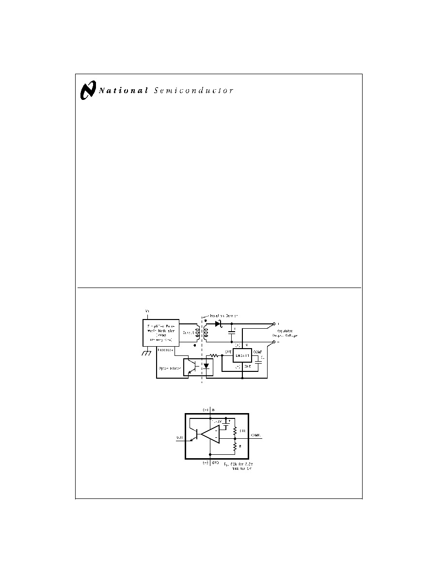
Typical Application and Functional Diagram
SIMPLE SWITCHER
TM
is a tradmark of National Semiconductor Corporation.
DS011987-1
Basic Isolated DC/DC Converter
DS011987-2
LM3411 Functional Diagram
December 1999
LM341
1
Precision
Secondary
Regulator/Driver
© 1999 National Semiconductor Corporation
DS011987
www.national.com
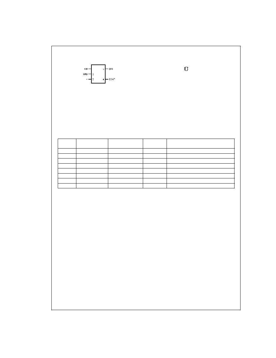
Connection Diagrams and Order Information
Five Lead Surface Mount Package Marking
and Order Information (SOT23-5)
The small SOT23-5 package allows only 4 alphanumeric characters to identify the product. The table below contains the field in-
formation marked on the package.
The first letter "D" identifies the part as a Driver, the next two numbers indicate the voltage, "00" for 3.3V part and "01" for a 5V
part. The fourth letter indicates the grade, "B" for standard grade, "A" for the prime grade.
The SOT23-5 surface mount package is only available on tape in quantities increments of 250 on tape and reel (indicated by the
letters "M5" in the part number), or in quantities increments of 3000 on tape and reel (indicated by the letters "M5X" in the part
number).
5-Lead Small Outline Package (M5)
DS011987-3
*No internal connection, but should be soldered to PC board for best heat
transfer.
Top View
Actual Size
DS011987-4
For Ordering Information
See
Figure 1 in this Data Sheet
See NS Package Number MA05B
Grade
Order Information
Package
Marking
Supplied as
3.3V
A (Prime)
LM3411AM5-3.3
D00A
1000 unit increments on tape and reel
3.3V
A (Prime)
LM3411AM5X-3.3
D00A
3000 unit increments on tape and reel
3.3V
B (Standard)
LM3411M5-3.3
D00B
1000 unit increments on tape and reel
3.3V
B (Standard)
LM3411M5X-3.3
D00B
3000 unit increments on tape and reel
5.0V
A (Prime)
LM3411AM5-5.0
D01A
1000 unit increments on tape and reel
5.0V
A (Prime)
LM3411AM5X-5.0
D01A
3000 unit increments on tape and reel
5.0V
B (Standard)
LM3411M5-5.0
D01B
1000 unit increments on tape and reel
5.0V
B (Standard)
LM3411M5X-5.0
D01B
3000 unit increments on tape and reel
FIGURE 1. SOT23-5 Marking and Order Information
LM341
1
www.national.com
2
Absolute Maximum Ratings
(Note 1)
If Military/Aerospace specified devices are required,
please contact the National Semiconductor Sales Office/
Distributors for availability and specifications.
Input Voltage V(IN)
20V
Output Current
20 mA
Junction Temperature
150∞C
Storage Temperature
-65∞C to +150∞C
Lead Temperature
Vapor Phase (60 sec.)
+215∞C
Infrared (15 sec.)
+220∞C
Power Dissipation (T
A
= 25∞C) (Note
2)
300 mW
ESD Susceptibility (Note 3)
Human Body Model
1500V
See AN-450 "Surface Mounting Methods and Their Effect on
Product Reliability" for methods on soldering surface-mount
devices.
Operating Ratings
(Notes 1, 2)
Ambient Temperature Range
-40∞C
T
A
+85∞C
Junction Temperature Range
-40∞C
T
J
+125∞C
Output Current
15 mA
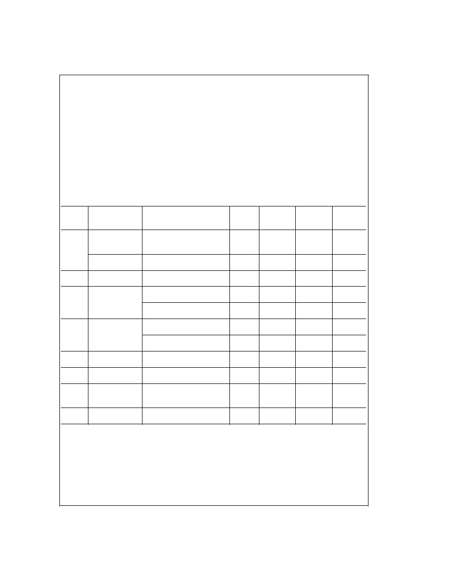
LM3411-3.3 Electrical Characteristics
Specifications with standard type face are for T
J
= 25∞C, and those with boldface type apply over full Operating Tempera-
ture Range. Unless otherwise specified, V(IN) = V
REG
, V
OUT
= 1.5V.
Symbol
Parameter
Conditions
Typical
LM3411A-3.3
LM3411-3.3
Units
(Note 4)
Limit
Limit
(Limits)
(Note 5)
(Note 5)
V
REG
Regulation Voltage
I
OUT
= 5 mA
3.3
V
3.317/3.333
3.333/3.366
V(max)
3.284/3.267
3.267/3.234
V(min)
Regulation Voltage
I
OUT
= 5 mA
±
0.5/
±
1
±
1/
±
2
%(max)
Tolerance
I
q
Quiescent Current
I
OUT
= 5 mA
85
µA
110/115
125/150
µA(max)
G
m
Transconductance
20 µA
I
OUT
1 mA
3.3
mA/mV
I
OUT
/
V
REG
1.5/0.75
1/0.50
mA/mV(min)
1 mA
I
OUT
15 mA
6.0
mA/mV
3.3/2.0
2.5/1.7
mA/mV(min)
A
V
Voltage Gain
1V
V
OUT
V
REG
- 1.2V (-1.3)
1000
V/V
V
OUT
/
V
REG
R
L
= 140
(Note 6)
550/250
450/200
V/V(min)
1V
V
OUT
V
REG
- 1.2V (-1.3)
3500
V/V
R
L
= 2 k
1500/900
1000/700
V/V(min)
V
SAT
Output Saturation
V(IN) = V
REG
+100 mV
1.0
V
(Note 7)
I
OUT
= 15 mA
1.2/1.3
1.2/1.3
V(max)
I
L
Output Leakage
V(IN) = V
REG
-100 mV
0.1
µA
Current
V
OUT
= 0V
0.5/1.0
0.5/1.0
µA(max)
R
f
Internal Feedback
52
k
Resistor (Note 8)
65
65
k
(max)
39
39
k
(min)
E
n
Output Noise
I
OUT
= 1 mA, 10 Hz
f
10 kHz
50
µV
RMS
Voltage
LM341
1
www.national.com
3
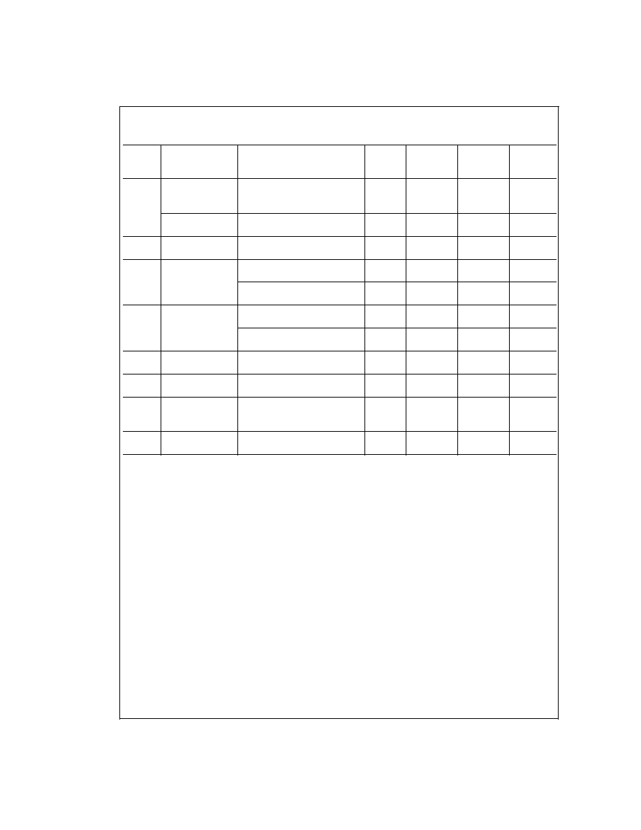
LM3411-5.0 Electrical Characteristics
Specifications with standard type face are for T
J
= 25∞C, and those with boldface type apply over full Operating Tempera-
ture Range. Unless otherwise specified, V(IN) = V
REG
, V
OUT
= 1.5V.
Symbol
Parameter
Conditions
Typical
LM3411A-5.0
LM3411-5.0
Units
(Note 4)
Limit
Limit
(Limits)
(Note 5)
(Note 5)
V
REG
Regulation Voltage
I
OUT
= 5 mA
5
V
5.025/5.050
5.050/5.100
V(max)
4.975/4.950
4.950/4.900
V(min)
Regulation Voltage
I
OUT
= 5 mA
±
0.5/
±
1
±
1/
±
2
%(max)
Tolerance
I
q
Quiescent Current
I
OUT
= 5 mA
85
µA
110/115
125/150
µA(max)
G
m
Transconductance
20 µA
I
OUT
1 mA
3.3
mA/mV
I
OUT
/
V
REG
1.5/0.75
1.0/0.5
mA/mV(min)
1 mA
I
OUT
15 mA
6.0
mA/mV
3.3/2.0
2.5/1.7
mA/mV(min)
A
V
Voltage Gain
1V
V
OUT
V
REG
- 1.2V (-1.3)
1000
V/V
V
OUT
/
V
REG
R
L
= 250
(Note 6)
750/350
650/300
V/V(min)
1V
V
OUT
V
REG
- 1.2V (-1.3)
3500
V/V
R
L
= 2 k
1500/900
1000/700
V/V(min)
V
SAT
Output Saturation
V(IN) = V
REG
+100 mV
1.0
V
(Note 7)
I
OUT
= 15 mA
1.2/1.3
1.2/1.3
V(max)
I
L
Output Leakage
V(IN) = V
REG
-100 mV
0.1
µA
Current
V
OUT
= 0V
0.5/1.0
0.5/1.0
µA(max)
R
f
Internal Feedback
94
k
Resistor (Note 8)
118
118
k
(max)
70
70
k
(min)
E
n
Output Noise
I
OUT
= 1 mA, 10 Hz
f
10 kHz
80
µV
RMS
Voltage
Note 1: Absolute Maximum Ratings indicate limits beyond which damage to the device may occur. Operating Ratings indicate conditions for which the device is in-
tended to be functional, but do not guarantee specific performance limits. For guaranteed specifications and test conditions, see the Electrical Characteristics. The
guaranteed specifications apply only for the test conditions listed. Some performance characteristics may degrade when the device is not operated under the listed
test conditions.
Note 2: The maximum power dissipation must be derated at elevated temperatures and is dictated by T
Jmax
(maximum junction temperature),
JA
(junction to am-
bient thermal resistance), and T
A
(ambient temperature). The maximum allowable power dissipation at any temperature is (P
Dmax
= T
Jmax
- T
A
)/
JA
or the number
given in the Absolute Maximum Ratings, whichever is lower. The typical thermal resistance (
JA
) when soldered to a printed circuit board is approximately 306∞C/W
for the M5 package.
Note 3: The human body model is a 100 pF capacitor discharged through a 1.5 k
resistor into each pin.
Note 4: Typical numbers are at 25∞C and represent the most likely parametric norm.
Note 5: Limits are 100% production tested at 25∞C. Limits over the operating temperature range are guaranteed through correlation using Statistical Quality Control
(SQC) methods. The limits are used to calculate National's Averaging Outgoing Level (AOQL).
Note 6: Actual test is done using equivalent current sink instead of a resistor load.
Note 7: V
SAT
= V(IN) - V
OUT
, when the voltage at the IN pin is forced 100 mV above the nominal regulating voltage (V
REG
).
Note 8: See Applications and Curves sections for information on this resistor.
LM341
1
www.national.com
4
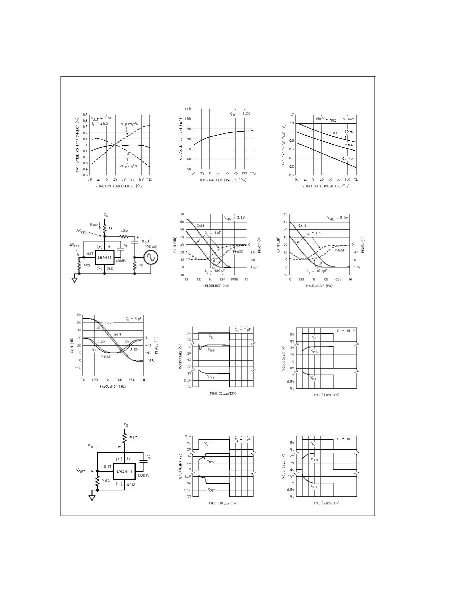
Typical Performance Characteristics
Normalized
Temperature Drift
DS011987-30
Quiescent Current
DS011987-31
Output Saturation
Voltage (V)
SAT
DS011987-32
Circuit Used for Bode Plots
DS011987-8
Bode Plot
DS011987-33
Bode Plot
DS011987-34
Bold Plot
DS011987-44
Response Time
for 3.3V Version
(C
C
= 0 pF)
DS011987-35
Response Time
for 3.3V Version
(C
C
= 10 nF)
DS011987-36
Circuit Used for Response Time
DS011987-11
Response Time
for 5V Version
(C
C
= 0 pF)
DS011987-37
Response Time
for 5V Version
(C
C
= 10 nF)
DS011987-38
LM341
1
www.national.com
5