 | –≠–ª–µ–∫—Ç—Ä–æ–Ω–Ω—ã–π –∫–æ–º–ø–æ–Ω–µ–Ω—Ç: LM3475MF | –°–∫–∞—á–∞—Ç—å:  PDF PDF  ZIP ZIP |

LM3475
Hysteretic PFET Buck Controller
General Description
The LM3475 is a hysteretic P-FET buck controller designed
to support a wide range of high efficiency applications in a
very small SOT23-5 package. The hysteretic control scheme
has several advantages, including simple system design
with no external compensation, stable operation with a wide
range of components, and extremely fast transient re-
sponse. Hysteretic control also provides high efficiency op-
eration, even at light loads. The PFET architecture allows for
low component count as well as 100% duty cycle and ultra-
low dropout operation.
Features
n
Easy to use control methodology
n
0.8V to V
IN
adjustable output range
n
High Efficiency (90% typical)
n
±
0.9% (
±
1.5% over temp) feedback voltage
n
100% duty cycle capable
n
Maximum operating frequency up to 2MHz
n
Internal Soft-Start
n
Enable pin
n
SOT23-5 package
Applications
n
TFT Monitor
n
Auto PC
n
Vehicle Security
n
Navigation Systems
n
Notebook Standby Supply
n
Battery Powered Portable Applications
n
Distributed Power Systems
Typical Application Circuit
20070101
October 2004
LM3475
Hysteretic
PFET
Buck
Controller
© 2004 National Semiconductor Corporation
DS200701
www.national.com
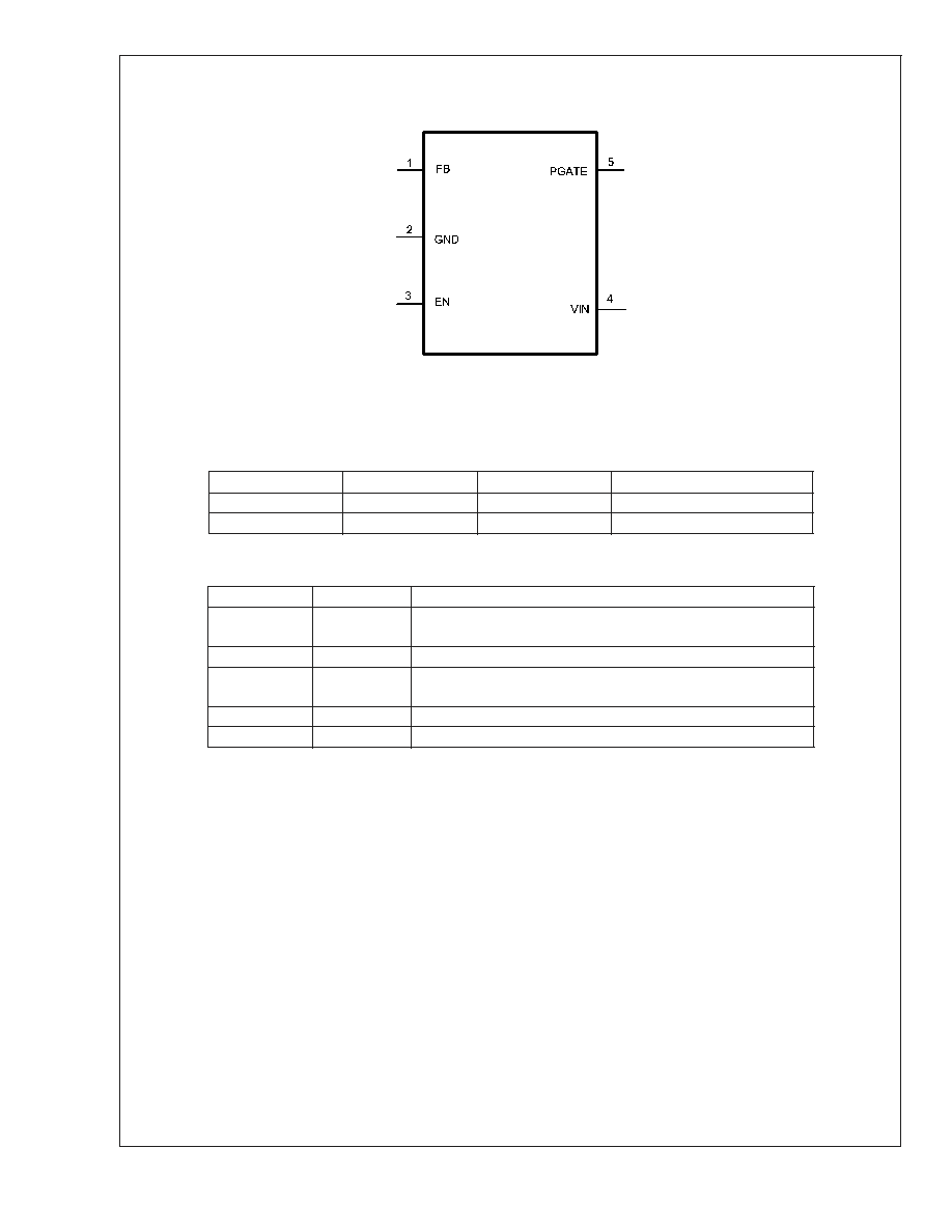
Connection Diagram
Top View
20070102
5 Lead Plastic SOT23-5
NS package Number MF05A
Package Marking and Ordering Information
Order Number
Package Type
Package Marking
Supplied As:
LM3475MF
SOT23-5
S65B
1000 units on Tape and Reel
LM3475MFX
SOT23-5
S65B
3000 units on Tape and Reel
Pin Description
Pin Name
Pin Number
Description
FB
1
Feedback input. Connect to a resistor divider between the output
and GND.
GND
2
Ground.
EN
3
Enable. Pull this pin above 1.5V (typical) for normal operation.
When EN is low, the device enters shutdown mode.
VIN
4
Power supply input.
PGATE
5
Gate drive output for the external PFET.
LM3475
www.national.com
2

Absolute Maximum Ratings
(Note 1)
If Military/Aerospace specified devices are required,
please contact the National Semiconductor Sales Office/
Distributors for availability and specifications.
V
IN
-0.3V to 16V
PGATE
-0.3V to 16V
FB
-0.3V to 5V
EN
-0.3V to 16V
Storage Temperature
-65∞C to 150∞C
Power Dissipation (Note 2)
440mW
ESD Susceptibilty
Human Body Model (Note 3)
2.5kV
Lead Temperature
Vapor Phase (60 sec.)
Infared (15 sec.)
215∞C
220∞C
Operating Ratings
(Note 1)
Supply Voltage
2.7V to 10V
Operating Junction
Temperature
-40∞C to +125∞C
Electrical Characteristics
Specifications in Standard type face are for T
J
= 25∞C, and in bold type face apply over the full Operating Temperature
Range (T
J
= -40∞C to +125∞C). Unless otherwise specified, V
IN
= EN = 5.0V. Datasheet min/max specification limits are guar-
anteed by design, test, or statistical analysis.
Symbol
Parameter
Conditions
Min
Typ
Max
Unit
I
Q
Quiescent Current
EN = V
IN
(PGATE
Open)
170
260
320
µA
EN = 0V
4
7
10
V
FB
Feedback Voltage
0.788
0.8
0.812
V
%
V
FB
/
V
IN
Feedback Voltage
Line Regulation
2.7V
<
V
IN
<
10V
0.01
%/V
V
HYST
Comparator
Hysteresis
2.7V
<
V
IN
<
10V
-40∞C to +125∞C
21
21
28
32
mV
I
FB
FB Bias Current
50
600
nA
Vth
EN
Enable Threshold
Voltage
Increasing
1.2
1.5
1.8
V
Hysteresis
365
mV
I
EN
Enable Leakage
Current
EN = 10V
.025
1
µA
R
PGATE
Driver Resistance
Source
I
SOURCE
= 100mA
2.8
Sink
I
Sink
= 100mA
1.8
I
PGATE
Driver Output Current
Source
V
PGATE
= 3.5V
C
PGATE
= 1nF
0.475
A
Sink
V
PGATE
= 3.5V
C
PGATE
= 1nF
1.0
T
SS
Soft-Start Time
2.7V
<
V
IN
<
10V
(EN Rising)
4
ms
T
ONMIN
Minimum On-Time
PGATE Open
180
ns
V
UVD
Under Voltage
Detection
Measured at the FB
Pin
0.487
0.56
0.613
V
LM3475
www.national.com
3

Electrical Characteristics
(Continued)
Note 1: Absolute maximum ratings are limits beyond which damage to the device may occur. Operating Ratings are conditions for which the device is intended to
be functional, but device parameter specifications may not be guaranteed. For guaranteed specifications and test conditions, see the Electrical Characteristics.
Note 2: The maximum allowable power dissipation is a function of the maximum junction temperature, T
J_MAX
, the junction-to-ambient thermal resistance,
JA
and
the ambient temperature, T
A
. The maximum allowable power dissipation at any ambient temperature is calculated using:
P
D_MAX
= (T
J_MAX
- T
A
)/
JA
. The maximum power dissipation of 0.44W is determined using T
A
= 25∞C,
JA
= 225∞C/W, and T
J_MAX
= 125∞C.
Note 3: The human body model is a 100 pF capacitor discharged through a 1.5k
resistor into each pin.
LM3475
www.national.com
4

Typical Performance Characteristics
Unless specified otherwise, all curves taken at V
IN
= 5V,
V
OUT
= 2.5V, L = 10 µH, C
OUT
= 100 µF, ESR = 100m
, and T
A
= 25∞C.
Quiescent Current vs Input Voltage
Feedback Voltage vs Temperature
20070122
20070123
Hysteresis Voltage vs Input Voltage
Hysteresis Voltage vs Temperature
20070124
20070125
Efficiency vs Load Current
Efficiency vs Input Voltage
I
OUT
= 2A
20070126
20070127
LM3475
www.national.com
5