LM3477/LM3477A
High Efficiency High-Side N-Channel Controller for
Switching Regulator
General Description
The LM3477/A is a high-side N-channel MOSFET switching
regulator controller. It can be used in topologies requiring a
high side MOSFET such as buck, inverting (buck-boost) and
zeta regulators. The LM3477/A's internal push pull driver
allows compatibility with a wide range of MOSFETs. This, the
wide input voltage range, use of discrete power components
and adjustable current limit allows the LM3477/A to be opti-
mized for a wide variety of applications.
The LM3477/A uses a high switching frequency of 500kHz to
reduce the overall solution size. Current-mode control re-
quires only a single resistor and capacitor for frequency
compensation. The current mode architecture also yields
superior line and load regulation and cycle-by-cycle current
limiting. A 5µA shutdown state can be used for power sav-
ings and for power supply sequencing. Other features in-
clude internal soft-start and output over voltage protection.
The internal soft-start reduces inrush current. Over voltage
protection is a safety feature to ensure that the output volt-
age stays within regulation.
The LM3477A is similar to the LM3477. The primary differ-
ence between the two is the point at which the device
transitions into hysteretic mode. The hysteretic threshold of
the LM3477A is one-third of the LM3477.
Features
n
500kHz switching frequency
n
Adjustable current limit
n
1.5% reference
n
Thermal shutdown
n
Frequency compensation optimized with a single
capacitor and resistor
n
Internal softstart
n
Current mode operation
n
Undervoltage lockout with hysteresis
n
8-lead Mini-SO8 (MSOP-8) package
Applications
n
Local Voltage Regulation
n
Distributed Power
n
Notebook and Palmtop Computers
n
Internet Appliances
n
Printers and Office Automation
n
Battery operated Devices
n
Cable Modems
n
Battery Chargers
Hysteretic
Threshold
LM3477
) 36% of
programmed current
limit
LM3477A
) 12% of
programmed current
limit
*See Hysteretic Threshold and section for more information.
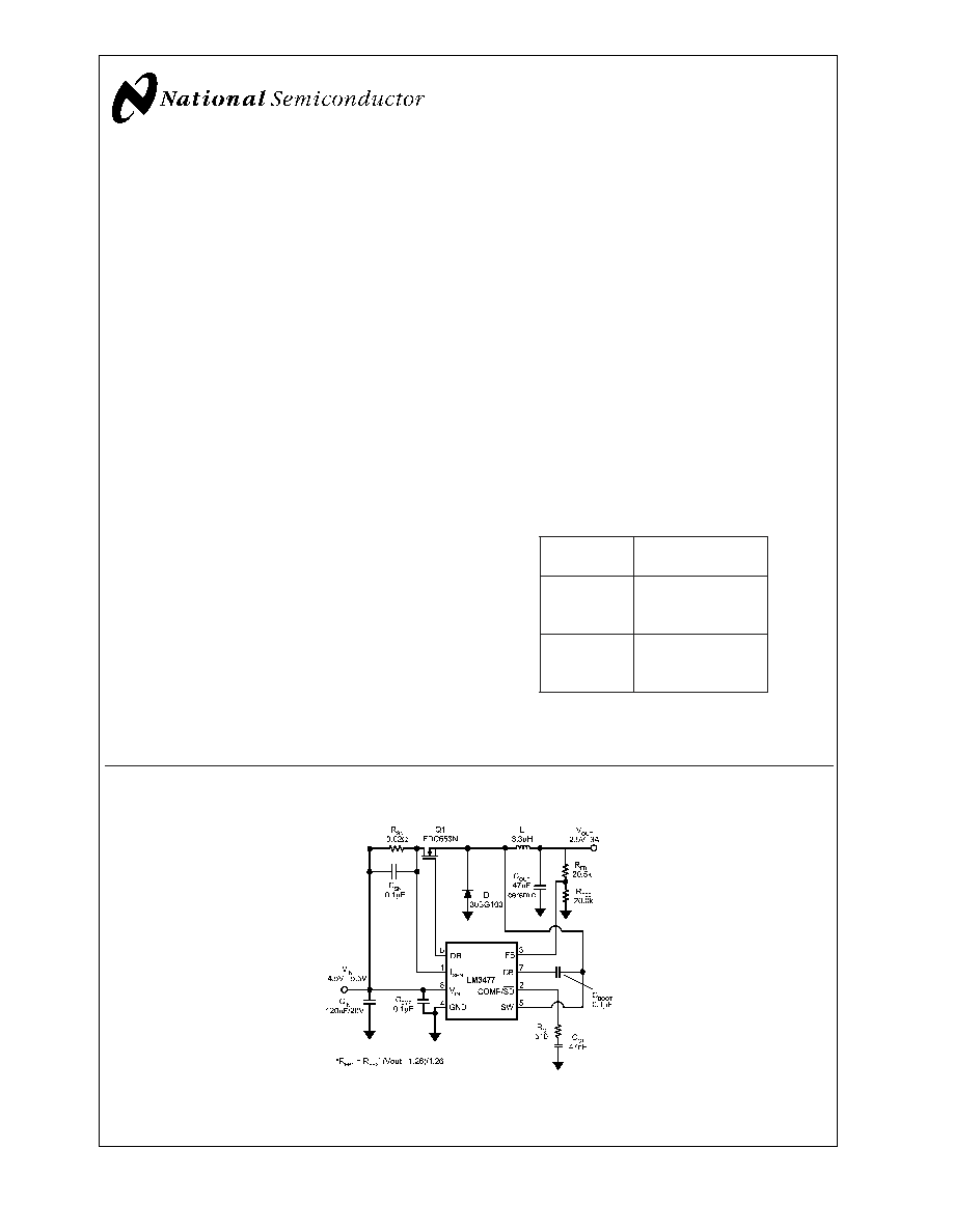
Typical Application Circuit
20003333
Typical High Efficiency Step-Down (Buck) Converter
June 2002
LM3477/LM3477A
High
Efficiency
High-Side
N-Channel
Controller
for
Switching
Regulator
© 2002 National Semiconductor Corporation
DS200033
www.national.com
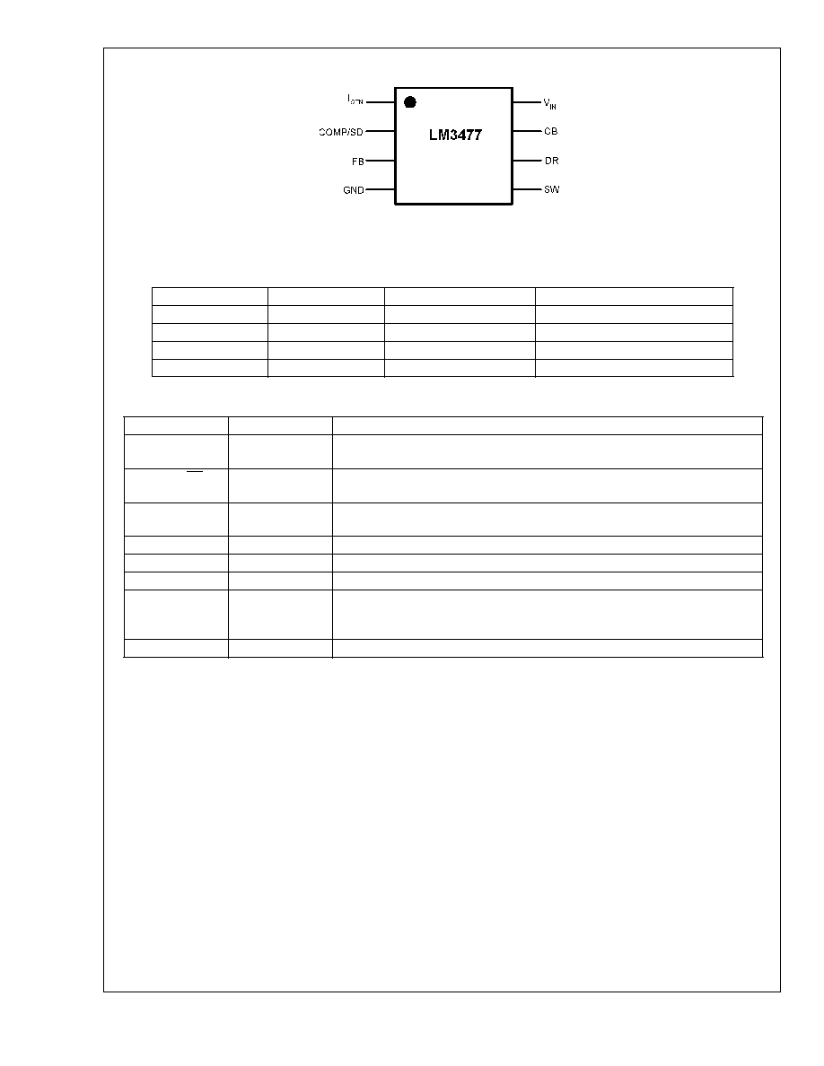
Connection Diagram
20003302
8 Lead Mini SO8 Package (MSOP-8 Package)
Package Marking and Ordering Information
Order Number
Package Type
Package Marking
Supplied As:
LM3477MM
MSOP-8
S13B
1000 units on Tape and Reel
LM3477MMX
MSOP-8
S13B
3500 units on Tape and Reel
LM3477AMM
MSOP-8
S13A
1000 units on Tape and Reel
LM3477AMMX
MSOP-8
S13A
3500 units on Tape and Reel
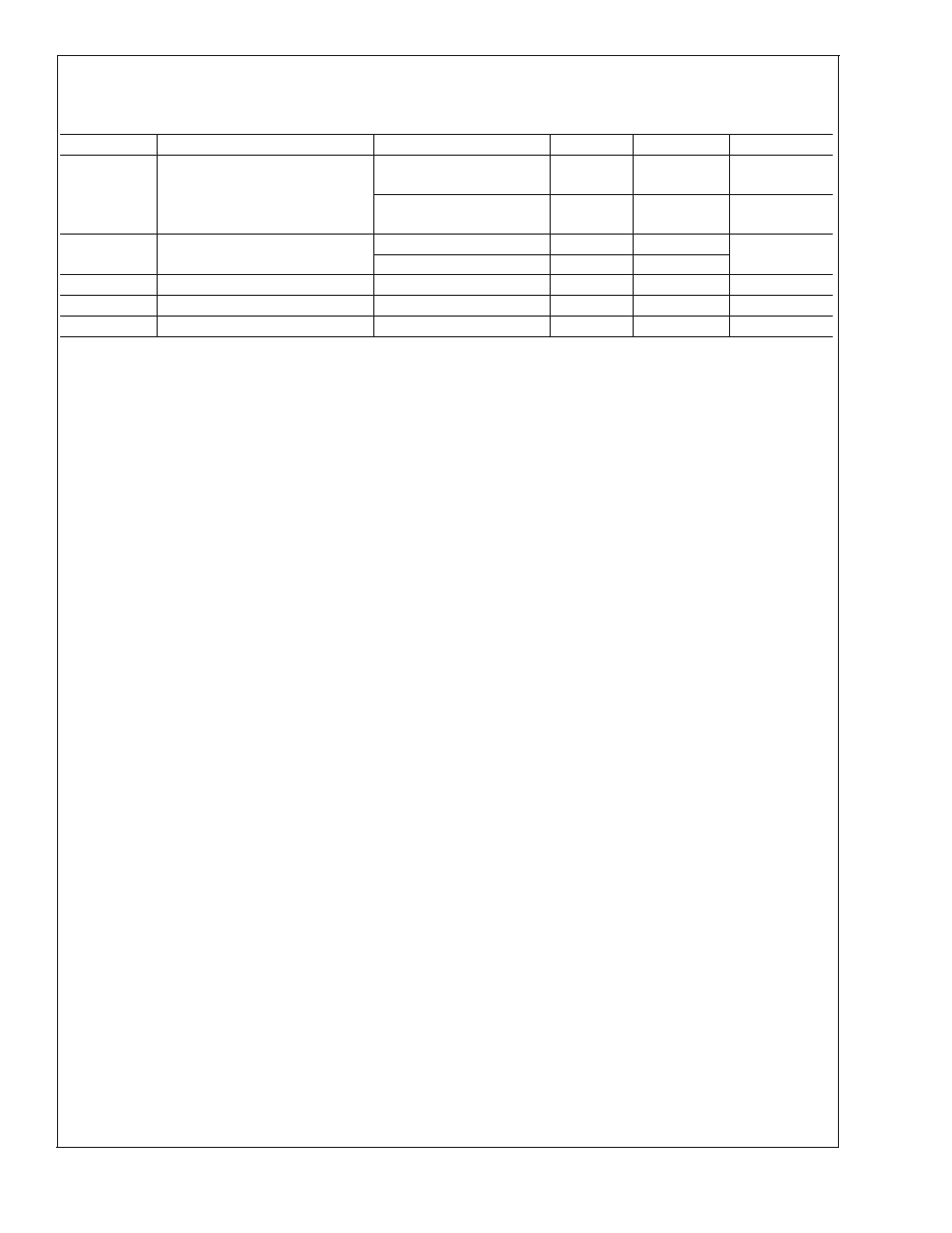
Pin Description
Pin Name
Pin Number
Description
I
SEN
1
Current sense input pin. Voltage generated across an external sense resistor is fed
into this pin.
COMP/SD
2
Compensation pin. A resistor-capacitor combination connected to this pin provides
compensation for the control loop. Pull this pin below 0.65V to shutdown.
FB
3
Feedback pin. The output voltage should be adjusted using a resistor divider to
provide 1.270V at this pin.
GND
4
Ground pin.
SW
5
Switch Node. Source of the external MOSFET is connected to this node.
DR
6
Drive pin. The gate of the external MOSFET should be connected to this pin.
CB
7
Boot-strap pin. A capacitor must be connected between this pin and SW pin (pin 5)
for proper operation. The voltage developed across this capacitor provides the gate
drive for the external MOSFET.
V
IN
8
Power Supply Input pin.
LM3477/LM3477A
www.national.com
2
Absolute Maximum Ratings
(Note 1)
If Military/Aerospace specified devices are required,
please contact the National Semiconductor Sales Office/
Distributors for availability and specifications.
Input Voltage
36V
Peak Driver Output Current (
<
10µs)
1.0A
CB Pin Voltage (Note 2)
43V
I
SEN
Pin Voltage
500mV
Power Dissipation
Internally Limited
Storage Temperature Range
-65∞C to +150∞C
Junction Temperature
+150∞C
ESD Susceptibilty (Note 3)
Human Body Model
Machine Model
2kV
200V
Lead Temperature for MSOP Package
Vapor Phase (60 sec.)
Infared (15 sec.)
215∞C
220∞C
Operating Ratings
(Note 1)
Supply Voltage
2.97V
V
IN
35V
Junction
Temperature Range
-40∞C
T
J
+125∞C
Electrical Characteristics
(Note 4)
Specifications in Standard type face are for T
J
= 25∞C, and in bold type face apply over the full Operating Temperature
Range. Unless otherwise specified, V
IN
= 12V.
Symbol
Parameter
Conditions
Typical
Limit
Units
V
FB
Feedback Voltage
V
COMP
= 1.4V,
2.97V
V
IN
36V
1.270
1.260/1.252
1.288/1.290
V
V(min)
V(max)
V
LINE
Feedback Voltage Line
Regulation
2.97V
V
IN
36V
0.001
%/V
V
LOAD
Output Voltage Load Regulation
±
0.5
%/V (max)
V
UVLO
Input Undervoltage Lock-out
2.87
2.97
V
V(max)
V
UV(HYS)
Input Undervoltage Lock-out
Hysteresis
180
130
225
mV
mV (min)
mV (max)
F
SW
Switching Frequency
500
435
575
kHz
kHz(min)
kHz(max)
R
DS1 (ON)
Driver Switch On Resistance
(top)
I
DR
= 0.2A, V
IN
= 5V
7
R
DS2 (ON)
Driver Switch On Resistance
(bottom)
I
DR
= 0.2A
4
(V
CB
-V
SW
)
max
Maximum Boot Voltage
V
IN
<
7.2V
V
IN
V
V
IN
7.2V
7.2
D
max
Maximum Duty Cycle
93
88
%
%(min)
T
min
(on)
Minimum On Time
330
230
495
nsec
nsec(min)
nsec(max)
I
SUPPLY
Supply Current (switching)
(Note 5)
2.0
3.0
mA
mA (max)
I
Q
Quiescent Current in Shutdown
Mode
(Note 6), V
IN
= 5V
5
8
µA
µA (max)
LM3477/LM3477A
www.national.com
3
Electrical Characteristics
(Note 4)
(Continued)
Specifications in Standard type face are for T
J
= 25∞C, and in bold type face apply over the full Operating Temperature
Range. Unless otherwise specified, V
IN
= 12V.
Symbol
Parameter
Conditions
Typical
Limit
Units
V
CL(O)
Current Limit Voltage at 0% Duty
Cycle
LM3477
155
130/125
185/190
mV
mV (min)
mV (max)
LM3477A
165
140/135
195/200
mV
mV (min)
mV (max)
V
CL(100)
Current Limit Voltage at 100%
Duty Cycle
LM3477
74
50/43
98/98
mV
mV (min)
mV (max)
LM3477A
65
41/25
89/98
mV
mV (min)
mV (max)
V
SC
Short-Circuit Current Limit Sense
Voltage
V
IN
= 5V, LM3477
350
270
420
mV
mV (min)
mV (max)
V
IN
= 5V, LM3477A
310
260
380
mV
mV (min)
mV (max)
V
SL
Internal Compensation Ramp
Voltage Height
V
IN
= 5V, LM3477
83
mV
V
IN
= 5V, LM3477A
103
V
OVP
Output Over-voltage Protection
(with respect to feedback
voltage) (Note 7)
V
COMP
= 1.4V
50
32/25
78/85
mV
mV(min)
mV(max)
V
OVP(HYS)
Output Over-Voltage Protection
Hysteresis(Note 7)
V
COMP
= 1.4V
60
20
110
mV
mV(min)
mV(max)
Gm
Error Amplifier
Transconductance
V
COMP
= 1.4V
I
EAO
= 100µA
(Source/Sink)
750
600/365
1000/1265
µmho
µmho (min)
µmho (max)
A
VOL
Error Amplifier Voltage Gain
V
COMP
= 1.4V
I
EAO
= 100µA
(Source/Sink)
38
30
42
V/V
V/V (min)
V/V (max)
I
EAO
Error Amplifier Output Current
(Source/ Sink)
Source, V
COMP
= 1.4V,
V
FB
= 0V
100
75/50
130/160
µA
µA (min)
µA (max)
Sink, V
COMP
= 1.4V, V
FB
= 1.4V
-140
-110/-95
-170/-180
µA
µA (min)
µA (max)
V
EAO
Error Amplifier Output Voltage
Swing
Upper Limit
V
FB
= 0V
COMP Pin = Floating
2.2
2.0
2.35
V
V(min)
V(max)
Lower Limit
V
FB
= 1.4V
0.75
0.5
0.95
V
V(min)
V(max)
T
SS
Internal Soft-Start Delay
V
FB
= 1.2V, V
COMP
=
Floating
5
msec
T
r
Drive Pin Rise Time
C
GS
= 3000pF, V
DR
= 0
to 3V
25
ns
T
f
Drive Pin Fall Time
C
GS
= 3000pF, V
DR
= 0
to 3V
25
ns
LM3477/LM3477A
www.national.com
4
Electrical Characteristics
(Note 4)
(Continued)
Specifications in Standard type face are for T
J
= 25∞C, and in bold type face apply over the full Operating Temperature
Range. Unless otherwise specified, V
IN
= 12V.
Symbol
Parameter
Conditions
Typical
Limit
Units
V
SD
Shutdown Threshold (Note 8)
Output = High
1.15
1.35
V
V (max)
Output = Low
0.65
0.3
V
V (min)
I
SD
Shutdown Pin Current
V
SD
= 5V
-1
µA
V
SD
= 0V
+1
TSD
Thermal Shutdown
165
∞C
T
SH
Thermal Shutdown Hysteresis
10
∞C
JA
Thermal Resistance
MM Package
200
∞C/W
LM3477/LM3477A
www.national.com
5