 | –≠–ª–µ–∫—Ç—Ä–æ–Ω–Ω—ã–π –∫–æ–º–ø–æ–Ω–µ–Ω—Ç: LM3485 | –°–∫–∞—á–∞—Ç—å:  PDF PDF  ZIP ZIP |
LM3485
Hysteretic PFET Buck Controller
General Description
The LM3485 is a high efficiency PFET switching regulator
controller that a system designer can use to quickly and
easily develop a small, low cost, switching buck regulator for
a wide range of applications. The use of a hysteretic control
scheme provides for simple design without any control loop
stability concerns using a wide variety of external compo-
nents. The PFET architecture also allows for low component
count as well as ultra-low dropout operation. Another benefit
is high efficiency operation at light loads without an increase
in output ripple. Current limit protection circuit is provided by
measuring the voltage across the PFET's R
DSON
thus elimi-
nating a costly sense resistor. The current limit can be ad-
justed allowing for designs at various output currents and
costs.
Features
n
Easy to use control methodology
n
No control loop compensation required
n
4.5V to 35V wide input range
n
1.242V to V
IN
adjustable output range
n
High Efficiency 93%
n
±
1.3% (
±
2% over temp) internal reference
n
100% duty cycle
n
Maximum operating frequency
>
1MHz
n
Current limit protection
n
MSOP-8
Applications
n
Set-Top Box
n
DSL/Cable Modem
n
PC/IA
n
Auto PC
n
TFT Monitor
n
Battery Powered Portable Applications
n
Distributed Power Systems
n
Always On Power
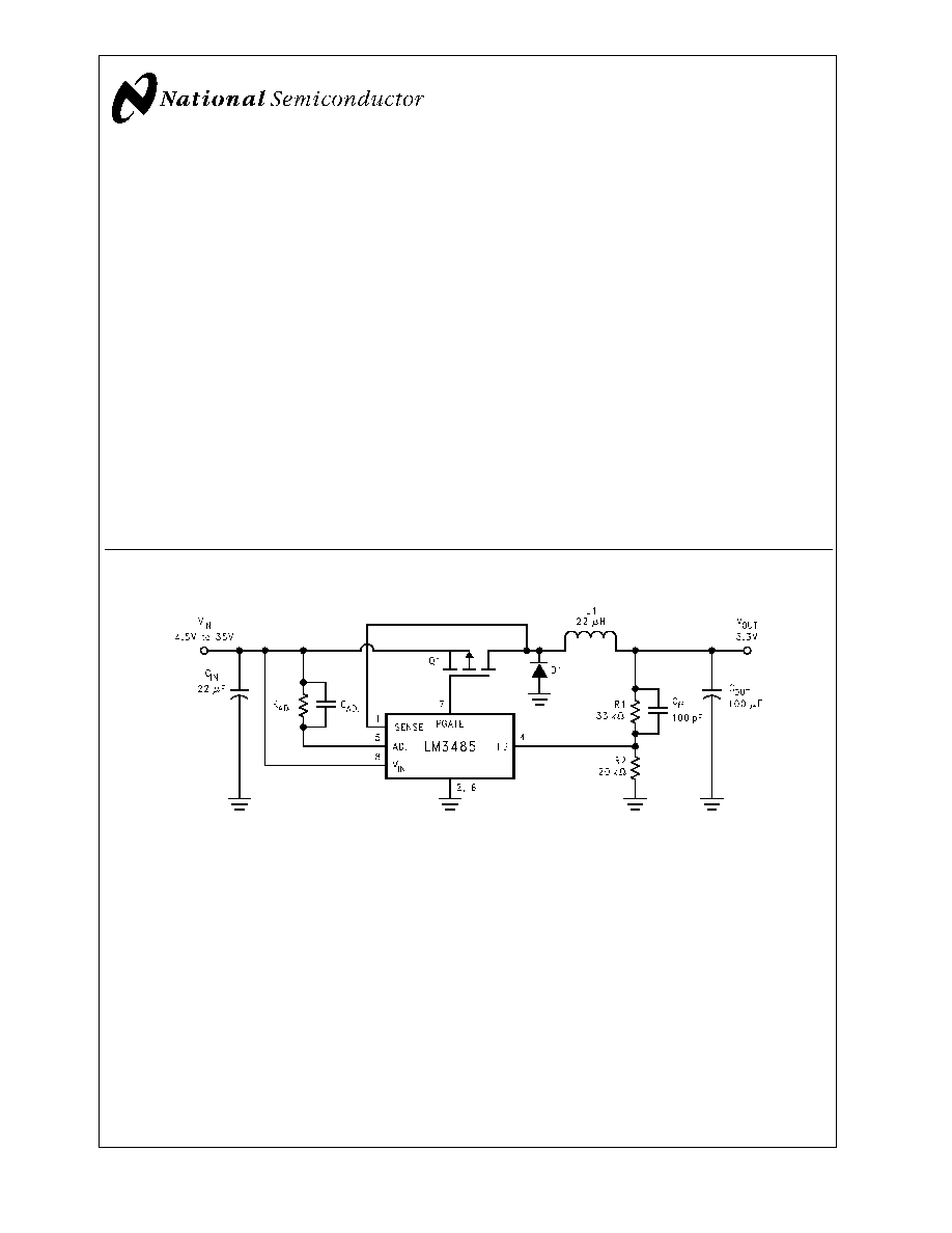
Typical Application Circuit
20034608
May 2002
LM3485
Hysteretic
PFET
Buck
Controller
© 2002 National Semiconductor Corporation
DS200346
www.national.com
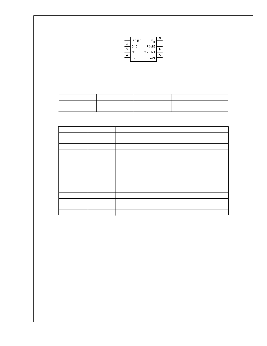
Connection Diagram
Top View
20034609
8 Lead Plastic MSOP-8
NS package Number MUA08A
Package Marking and Ordering Information
Order Number
Package Type
Package Marking
Supplied As:
LM3485MM
MSOP-8
S29B
1000 units on Tape and Reel
LM3485MMX
MSOP-8
S29B
3500 units on Tape and Reel
Pin Description
Pin Name
Pin Number
Description
ISENSE
1
The current sense input pin. This pin should be connected to Drain
node of the external PFET.
GND
2
Signal ground.
NC
3
No connection.
FB
4
The feedback input. Connect the FB to a resistor voltage divider
between the output and GND for an adjustable output voltage.
ADJ
5
Current limit threshold adjustment. It connects to an internal 5.5µA
current source. A resistor is connected between this pin and the
input Power Supply. The voltage across this resistor is compared
with the V
DS
of the external PFET to determine if an over-current
condition has occurred.
PWR GND
6
Power ground.
PGATE
7
Gate Drive output for the external PFET. PGATE swings between
V
IN
and V
IN
-5V.
VIN
8
Power supply input pin.
LM3485
www.national.com
2
Absolute Maximum Ratings
(Note 1)
If Military/Aerospace specified devices are required,
please contact the National Semiconductor Sales Office/
Distributors for availability and specifications.
VIN Voltage
-0.3V to 36V
PGATE Voltage
-0.3V to 36V
FB Voltage
-0.3V to 5V
ISENSE Voltage
-1.0V to 36V
ADJ Voltage
-0.3V to 36V
Maximum Junction Temp.
150∞C
Power Dissipation
417mW
@
T
A
=
25∞C
ESD Susceptibilty
Human Body Model (Note 3)
2kV
Lead Temperature
Vapor Phase (60 sec.)
Infared (15 sec.)
215∞C
220∞C
Storage Temperature
-65∞C to 150∞C
Operating Ratings
(Note 1)
Supply Voltage
4.5V to 35V
Operating Junction
Temperature
-40∞C to +125∞C
Electrical Characteristics
Specifications in Standard type face are for T
J
= 25∞C, and in bold type face apply over the full Operating Temperature
Range (T
J
= -40∞C to +125∞C). Unless otherwise specified, V
IN
= 12V, V
ISNS
= V
IN
- 1V, and V
ADJ
= V
IN
- 1.1V. Datasheet
min/max specification limits are guaranteed by design, test, or statistical analysis.
Symbol
Parameter
Conditions
Min
(Note 4)
Typ
(Note 5)
Max
(Note 4)
Unit
I
Q
Quiescent Current at
ground pin
FB = 1.5V
(Not Switching)
250
400
µA
V
FB
Feedback Voltage
(Note 6)
1.226
1.217
1.242
1.258
1.267
V
V
HYST
Comparator
Hysteresis
10
14
15
20
mV
V
CL
(Note 7)
Current limit
comparator trip
voltage
R
ADJ
= 20k
110
mV
R
ADJ
= 160k
880
V
CL_OFFSET
Current limit
comparator offset
V
FB
= 1.5V
-20
0
+20
mV
I
CL_ADJ
Current limit ADJ
current source
V
FB
= 1.5V
3.0
5.5
7.0
µA
T
CL
Current limit one shot
off time
V
ADJ
= 11.5V
V
ISNS
= 11.0V
V
FB
= 1.0V
6
9
14
µs
R
PGATE
Driver resistance
Source
I
SOURCE
= 100mA
5.5
Sink
I
Sink
= 100mA
8.5
I
PGATE
Driver Output current
Source
V
IN
= 7V,
P
GATE
= 3.5V
0.44
A
Sink
V
IN
= 7V,
P
GATE
= 3.5V
0.32
V
PGATEMIN
Minimum driver
voltage
V
IN
= 4.5V
V
FB
= 1.0V
I
GATE
= 100µA sink
1.2
V
I
FB
FB pin Bias Current
(Note 8)
V
FB
= 1.0V
300
750
nA
T
ONMIN_NOR
Minimum on time in
normal operation
V
ISNS
= V
ADJ
+0.1V
C
load
on OUT =
1000pF
(Note 9)
100
ns
LM3485
www.national.com
3
Electrical Characteristics
(Continued)
Specifications in Standard type face are for T
J
= 25∞C, and in bold type face apply over the full Operating Temperature
Range (T
J
= -40∞C to +125∞C). Unless otherwise specified, V
IN
= 12V, V
ISNS
= V
IN
- 1V, and V
ADJ
= V
IN
- 1.1V. Datasheet
min/max specification limits are guaranteed by design, test, or statistical analysis.
Symbol
Parameter
Conditions
Min
(Note 4)
Typ
(Note 5)
Max
(Note 4)
Unit
T
ONMIN_CL
Minimum on time in
current limit
V
ISNS
= V
ADJ
+0.1V
V
FB
= 1.0V C
load
on
OUT = 1000pF
(Note 9)
175
ns
%V
FB
/
V
IN
Feedback Voltage
Line Regulation
4.5
V
IN
35V
0.010
%/V
Note 1: Absolute maximum ratings are limits beyond which damage to the device may occur. Operating Ratings are conditions for which the device is intended to
be functional, but device parameter specifications may not be guaranteed. For guaranteed specifications and test conditions, see the Electrical Characteristics.
Note 2: The maximum allowable power dissipation is a function of the maximum junction temperature, T
J_MAX
, the junction-to-ambient thermal resistance,
JA
=
240∞C/W, and the ambient temperature, T
A
. The maximum allowable power dissipation at any ambient temperature is calculated using:
P
D_MAX
= (T
J_MAX
- T
A
)/
JA
. Exceeding the maximum allowable power dissipation will cause excessive die temperature.
Note 3: The human body model is a 100 pF capacitor discharged through a 1.5k
resistor into each pin.
Note 4: All limits are guaranteed at room temperature (standard type face) and at temperature extremes (bold type face). All room temperature limits are 100%
tested. All limits at temperature extremes are guaranteed via correlation using standard Statistical Quality Control (SQC) methods. All limits are used to calculate
Average Outgoing Quality Level (AOQL).
Note 5: Typical numbers are at 25∞C and represent the most likely norm.
Note 6: The V
FB
is the trip voltage at the FB pin when PGATE switches from high to low.
Note 7: V
CL
= I
CL_ADJ
*
R
ADJ
Note 8: Bias current flows out from the FB pin.
Note 9: A 1000pF capacitor is connected between V
IN
and PGATE.
LM3485
www.national.com
4
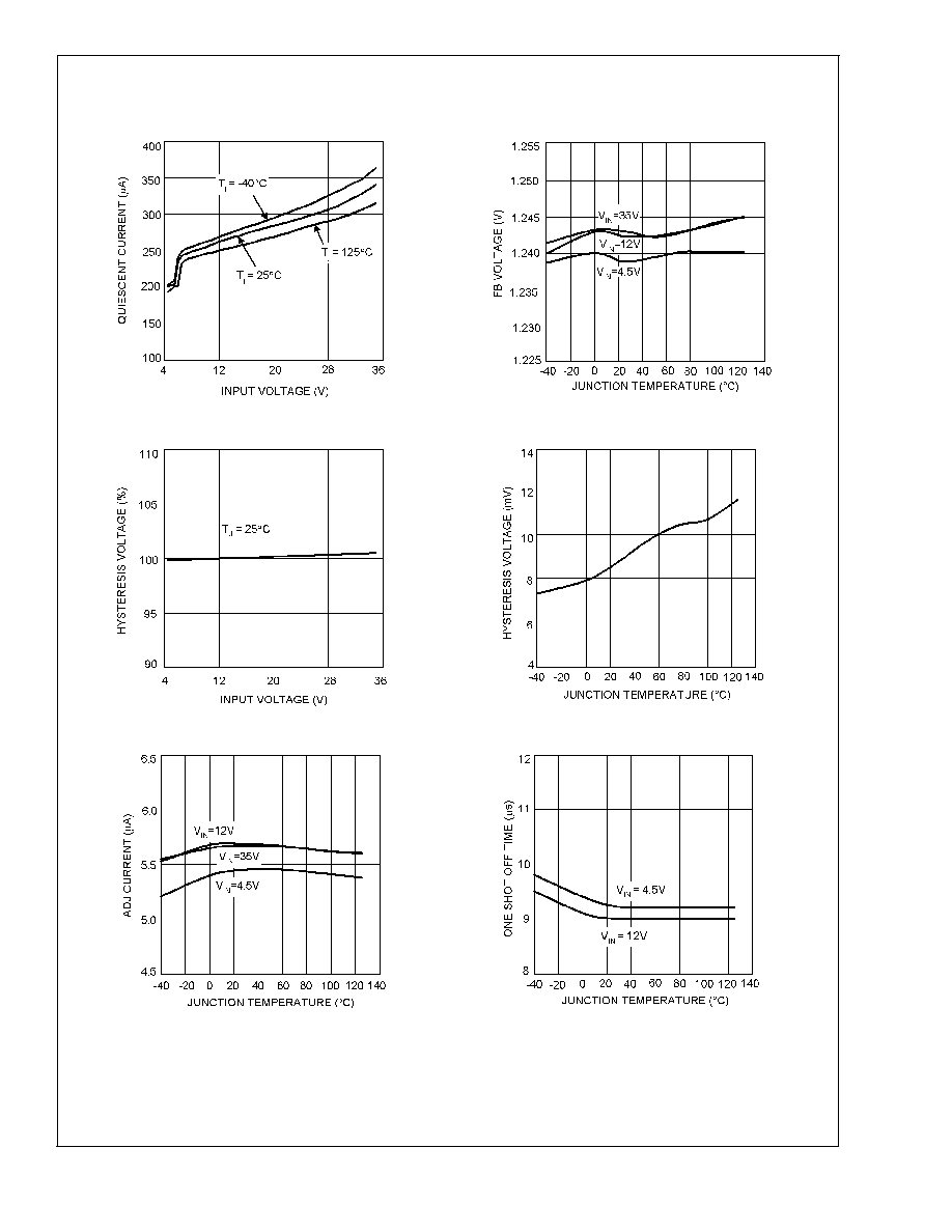
Typical Performance Characteristics
Unless otherwise specified, T
J
= 25∞C
Quiescent Current vs Input Voltage
(FB = 1.5V)
Feedback Voltage vs Temperature
20034601
20034607
Hysteresis Voltage vs Input Voltage
Hysteresis Voltage vs Temperature
20034605
20034606
Current Limit ADJ Current vs Temperature
Current Limit One Shot OFF Time vs. Temperature
20034602
20034604
LM3485
www.national.com
5
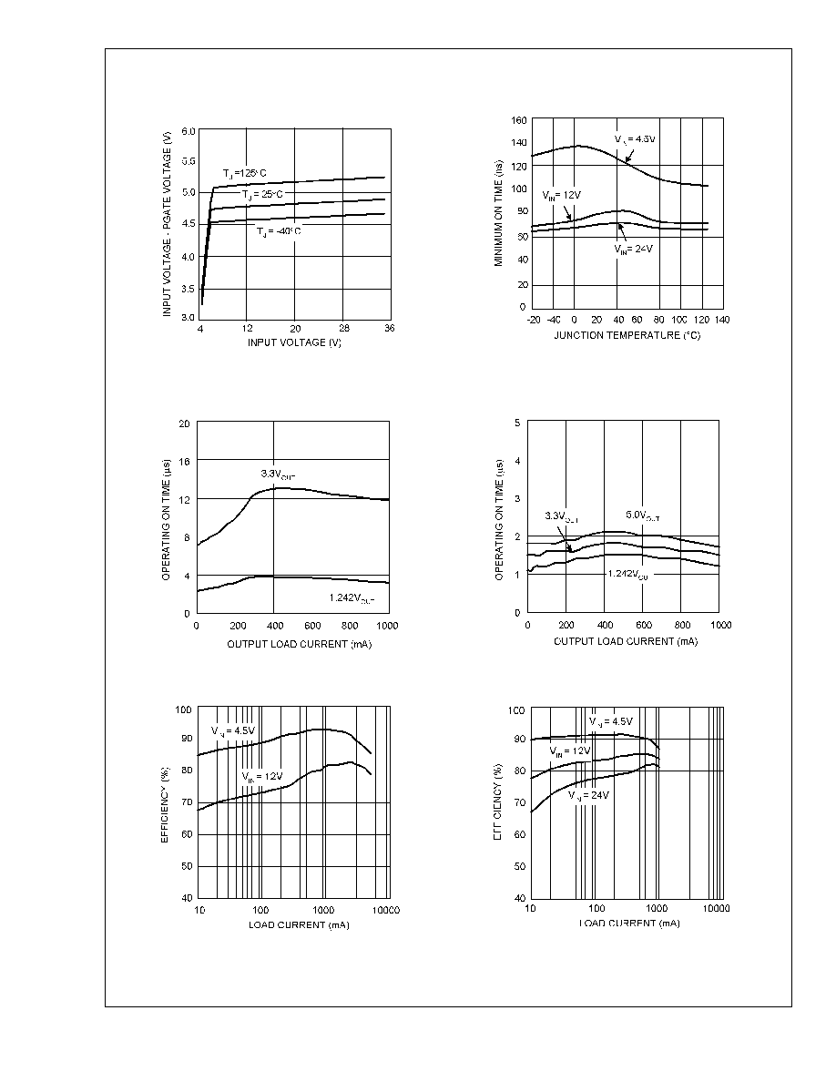
Typical Performance Characteristics
Unless otherwise specified, T
J
= 25∞C (Continued)
PGATE Voltage vs Input Voltage
Minimum ON Time vs. Temperature
20034603
20034612
Operating ON Time vs
Output Load Current
(V
IN
= 4.5V)
Operating ON Time vs
Output Load Current
(V
IN
= 12V)
20034622
20034640
Efficiency vs Load Current
(V
OUT
= 3.3V, L = 6.8µH)
Efficiency vs Load Current
(V
OUT
= 3.3V, L = 22µH)
20034617
20034618
LM3485
www.national.com
6
Typical Performance Characteristics
Unless otherwise specified, T
J
= 25∞C (Continued)
Efficiency vs Load Current
(V
OUT
= 5.0V, L = 22µH)
Start Up
20034631
20034620
Continuous Mode Operation
(V
IN
= 12V, V
OUT
= 3.3 V, I
OUT
= 500mA, L = 22µH)
Discontinuous Mode Operation
(V
IN
= 12V, V
OUT
=3.3 V, I
OUT
= 50mA, L = 22µH)
20034615
20034616
Operating Frequency vs Input Voltage
(V
OUT
= 3.3V, I
OUT
= 1A, C
OUT(ESR)
= 80m
, C
ff
= 100pF)
Output Ripple Voltage vs Input Voltage
(V
OUT
= 3.3V, I
OUT
= 1A, C
OUT(ESR)
= 80m
, C
ff
= 100pF)
20034613
20034643
LM3485
www.national.com
7
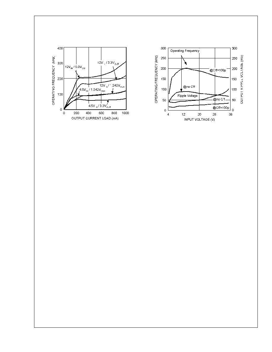
Typical Performance Characteristics
Unless otherwise specified, T
J
= 25∞C (Continued)
Operating Frequency vs
Output Load Current
(L = 22µH, C
OUT(ESR)
= 45m
, C
ff
= 100pF)
Feed-Forward Capacitor (Cff) Effect
(V
OUT
= 3.3V, L = 22µH, I
OUT
= 500mA)
20034621
20034630
LM3485
www.national.com
8

Block Diagram
20034610
Functional Description
Overview
The LM3485 is buck (step-down) DC-DC controller that uses
a hysteretic control scheme. The comparator is designed
with approximately 10mV of hysteresis. In response to the
voltage at the FB pin, the gate drive (PGATE pin) turns the
external PFET on or off. When the inductor current is too
high, the current limit protection circuit engages and turns
the PFET off for approximately 9µs.
The hysteretic control does not provide an internal oscillator.
Switching frequency depends on the external components
and operating conditions. Operating frequency reduces at
light loads resulting in excellent efficiency compared to other
architectures.
2 external resistors can easily program the output voltage.
The output can be set in a wide range from 1.242V to V
IN
.
Hysteretic Control Circuit
The LM3485 uses a comparator based voltage control loop.
The feedback is compared to a 1.242V reference and a
10mV hysteresis is designed into the comparator to ensure
noise free operation.
When the FB input to the comparator falls below the refer-
ence voltage, the output of the comparator moves to a low
state. This results in the driver output, PGATE, pulling the
gate of the PFET low and turning on the PFET. With the
PFET on, the input supply charges Cout and supplies cur-
rent to the load via the series path through the PFET and the
inductor. Current through the Inductor ramps up linearly and
the output voltage increases. As the FB voltage reaches the
upper threshold, which is the internal reference voltage plus
10mV, the output of the comparator changes from low to
high, and the PGATE responds by turning the PFET off. As
the PFET turns off, the inductor voltage reverses, the catch
diode turns on, and the current through the inductor ramps
down. Then, as the output voltage reaches the internal ref-
erence voltage again, the next cycle starts.
The LM3485 operates in discontinuous conduction mode at
light load current or continuous conduction mode at heavy
load current. In discontinuous conduction mode, current
through the inductor starts at zero and ramps up to the peak,
then ramps down to zero. Next cycle starts when the FB
voltage reaches the internal voltage. Until then, the inductor
current remains zero. Operating frequency is lower and
switching losses reduce. In continuous conduction mode,
current always flows through the inductor and never ramps
down to zero.
The output voltage (V
OUT
) can be programmed by 2 external
resistors. It can be calculated as following.
V
OUT
= 1.242
*
( R1 + R2 ) / R2
20034623
FIGURE 1. Hysteretic Window
LM3485
www.national.com
9
Functional Description
(Continued)
The minimum output voltage ripple (V
OUT_PP
) can be calcu-
lated in the same way.
V
OUT_PP
= V
HYST
( R1 + R2 ) / R2
For example, with V
OUT
set to 3.3V, V
OUT_PP
is 26.6mV
V
OUT_PP
= 0.01
*
( 33K + 20K ) / 20K = 0.0266V
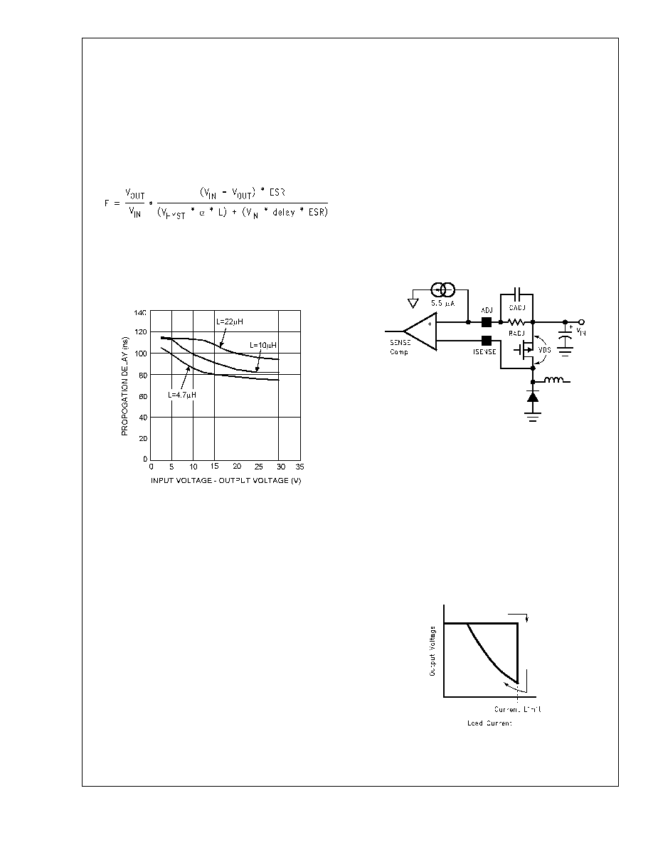
Operating frequency (F) is determined by knowing the input
voltage, output voltage, inductor, V
HYST
, ESR (Equivalent
Series Resistance) of output capacitor, and the delay. It can
be approximately calculated using the formula:
where:
: ( R1 + R2 ) / R2
delay: It includes the LM3485 propagation delay time
and
the PFET delay time. The propagation delay is 90ns
typically. (See the Propagation Delay curve below.)
The operating frequency and output ripple voltage can also
be significantly influenced by the speed up capacitor (Cff).
Cff is connected in parallel with the high side feedback
resistor, R1. The location of this capacitor is similar to where
a feed forward capacitor would be located in a PWM control
scheme. However it's effect on hysteretic operation is much
different. The output ripple causes a current to be sourced or
sunk through this capacitor. This current is essentially a
square wave. Since the input to the feedback pin, FB, is a
high impedance node, the current flows through R2. The end
result is a reduction in output ripple and an increase in
operating frequency. When adding Cff, calculate the formula
above with
= 1. The value of Cff depend on the desired
operating frequency and the value of R2. A good starting
point is 470pF ceramic at 100kHz decreasing linearly with
increased operating frequency. Also note that as the output
voltage is programmed below 2.5V, the effect of Cff will
decrease significantly.
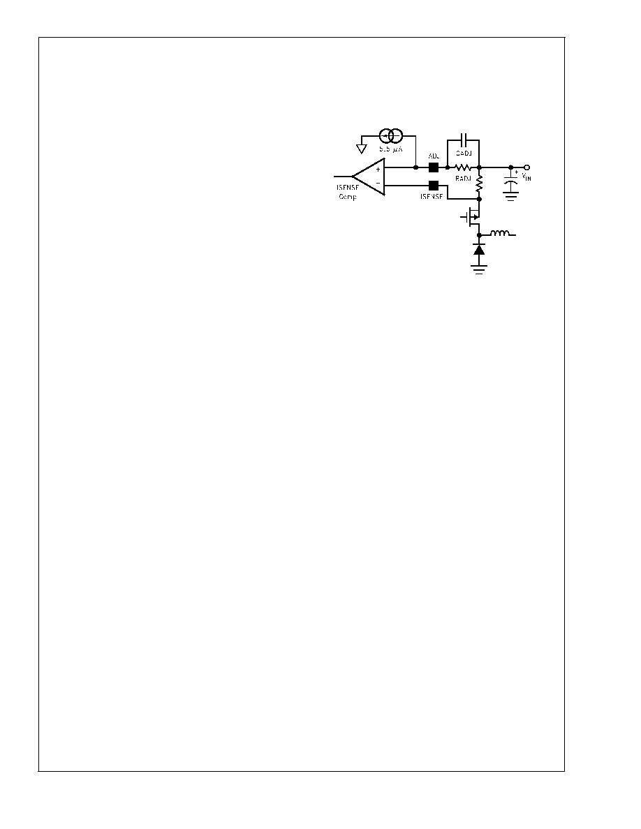
Current Limit Operation
The LM3485 has a cycle-by-cycle current limit. Current limit
is sensed across the V
DS
of the PFET or across an addi-
tional sense resistor. When current limit is reached, the
LM3485 turns off the external PFET for a period of 9µs. The
current limit is adjusted by an external resistor, R
ADJ
.
The current limit circuit is composed of the ISENSE com-
parator and the one-shot pulse generator. The positive input
of the ISENSE comparator is the ADJ pin. An internal 5.5µA
current sink creates a voltage across the external R
ADJ
resister. This voltage is compared to the voltage across the
PFET or sense resistor. The ADJ voltage can be calculated
as follows.
V
ADJ
= V
IN
- (R
ADJ
*
5.5µA)
The negative input of the ISENSE comparator is the ISENSE
pin that should be connected to the drain of the external
PFET. The inductor current is determined by sensing the
V
DS
. It can be calculated as follows.
V
ISENSE
= V
IN
- (R
DSON
*
I
IND_PEAK
) = V
IN
- V
DS
The current limit is activated when the voltage at the ISENSE
pin exceeds the voltage at the ADJ pin. The ISENSE com-
parator triggers the 9µs one shot pulse generator forcing the
driver to turn the PFET off. The driver turns the PFET back
on after 9µs. If the current has not reduced below the set
threshold, the cycle will repeat continuously.
During current limit operation, the output voltage will drop
significantly as will operating frequency. As the load current
is reduced, the output will return to the programmed voltage.
However, there is a current limit fold back phenomenon
inherent in this current limit architecture. See
Figure 4.
20034614
FIGURE 2. Propagation Delay
20034625
FIGURE 3. Current Sensing by V
DS
20034626
FIGURE 4. Current Limit Fold Back Phenomenon
LM3485
www.national.com
10
Functional Description
(Continued)
Start Up
The current limit circuit is active during start-up. During
start-up the PFET will stay on until either the current limit or
the feedback comparator is tripped
If the current limit comparator is tripped first then the fold
back characteristic should be taken into account. Start-up
into full load may require a higher current limit set point or the
load must be applied after start-up.
One problem with selecting a higher current limit is inrush
current during start-up. Adding a capacitance (C
ADJ
) in par-
allel with R
ADJ
results in soft-start. C
ADJ
and R
ADJ
create an
RC time constant forcing current limit to activate at a lower
current. The output voltage will ramp more slowly when
using the soft-start functionality.
The C
ADJ
also filters unwanted noise so that the ISENSE
comparator will not be accidentally triggered. A value of
100pF to 1nF is recommended in most applications. These
low values for C
ADJ
will have little to no effect on soft-start.
There are example start-up plots for C
ADJ
equal to 1nF and
10nF in the Typical Performance Characteristics.
External Sense Resistor
The V
DS
of a PFET will tend to vary significantly over tem-
perature. This will result an equivalent variation in current
limit. To improve current limit accuracy an external sense
resistor can be connected from V
IN
to the source of the
PFET, as shown in
Figure 5.
20034627
FIGURE 5. Current Sensing by External Resistor
LM3485
www.national.com
11
Design Information
Hysteretic control is a simple control scheme. However the
operating frequency and other performance characteristics
highly depend on external conditions and components. If
either the inductance, output capacitance, ESR, V
IN
, or Cff is
changed, there will be a change in the operating frequency
and output ripple. The best approach is to determine what
operating frequency is desirable in the application and then
begin with the selection of the inductor and C
OUT
ESR.
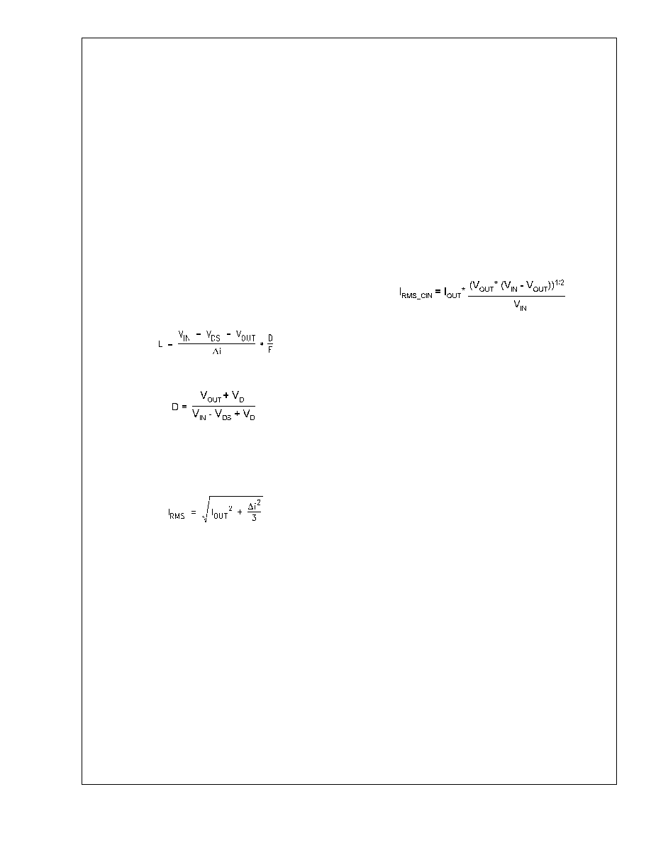
Inductor Selection (L1)
The important parameters for the inductor are the induc-
tance and the current rating. The LM3485 operates over a
wide frequency range and can use a wide range of induc-
tance values. A good rule of thumb is to use the equations
used for National's Simple Switchers
Æ
. The equation for
inductor ripple (
i) as a function of output current (I
OUT
) is:
for I
out
<
2.0Amps
i
I
out
*
0.386827
*
I
out
-0.366726
for I
out
>
2.0Amps
i
I
out
*
0.3
The inductance can be calculated based upon the desired
operating frequency where:
And
where D is the duty cycle and V
D
is the diode forward
voltage.
The inductor should be rated to the following:
Ipk = (Iout+
i/2)
*
1.1
The inductance value and the resulting ripple is one of the
key parameters controlling operating frequency. The second
is the ESR.
Output Capacitor Selection (C
OUT
)
The ESR of the output capacitor times the inductor ripple
current is equal to the output ripple of the regulator. How-
ever, the V
HYST
sets the first order value of this ripple. As
ESR is increased with a given inductance, then operating
frequency increases as well. If ESR is reduced then the
operating frequency reduces.
The use of ceramic capacitors has become a common de-
sire of many power supply designers. However, ceramic
capacitors have a very low ESR resulting in a 90∞ phase shift
of the output voltage ripple. This results in low operating
frequency and increased output ripple. To fix this problem a
low value resistor should be added in series with the ceramic
output capacitor. Although counter intuitive, this combination
of a ceramic capacitor and external series resistance provide
highly accurate control over the output voltage ripple. The
other types capacitor, such as Sanyo POS CAP and
OS-CON, Panasonic SP CAP, Nichicon 'NA' series, are also
recommended and may be used without additional series
resistance.
For all practical purposes, any type of output capacitor may
be used with proper circuit verification.
Input Capacitor Selection (C
IN
)
A bypass capacitor is required between the input source and
ground. It must be located near the source pin of the external
PFET. The input capacitor prevents large voltage transients
at the input and provides the instantaneous current when the
PFET turns on.
The important parameters for the input capacitor are the
voltage rating and the RMS current rating. Follow the manu-
facturer's recommended voltage derating. For high input
voltage application, low ESR electrolytic capacitor, the Nichi-
con 'UD' series or the Panasonic 'FK' series, is available.
The RMS current in the input capacitor can be calculated.
The input capacitor power dissipation can be calculated as
follows.
P
D(CIN)
= I
RMS_CIN
2
*
ESR
CIN
The input capacitor must be able to handle the RMS current
and the P
D
. Several input capacitors may be connected in
parallel to handle large RMS currents. In some cases it may
be much cheaper to use multiple electrolytic capacitors than
a single low ESR, high performance capacitor such as
OS-CON or Tantalum. The capacitance value should be
selected such that the ripple voltage created by the charge
and discharge of the capacitance is less than 10% of the
total ripple across the capacitor.
Programming the Current Limit (R
ADJ
)
The current limit is determined by connecting a resistor
(R
ADJ
) between input voltage and the ADJ pin.
R
ADJ
= I
IND_PEAK
*
R
DSON
/I
CL_ADJ
where:
R
DSON
: Drain-Source ON resistance of the external PFET
I
CL_ADJ
: 5.5µA typically
I
IND_PEAK
= I
LOAD
+ I
RIPPLE
/2
Catch Diode Selection (D1)
The important parameters for the catch diode are the peak
current, the peak reverse voltage, and the average power
dissipation. The average current through the diode can be
calculated as following.
I
D_AVE
= I
OUT
*
(1 - D)
The off state voltage across the catch diode is approximately
equal to the input voltage. The peak reverse voltage rating
must be greater than input voltage. In nearly all cases a
shottky diode is recommended. In low output voltage appli-
cations a low forward voltage provides improved efficiency.
For high temperature applications, diode leakage current
may become significant and require a higher reverse voltage
rating to achieve acceptable performance.
LM3485
www.national.com
12
Design Information
(Continued)
P-Channel MOSFET Selection (Q1)
The important parameters for the PFET are the maximum
Drain-Source voltage (V
DS
), the on resistance (R
DSON
), Cur-
rent rating, and the input capacitance.
The voltage across the PFET when it is turned off is equal to
the sum of the input voltage and the diode forward voltage.
The V
DS
must be selected to provide some margin beyond
the input voltage. PGATE swings the PFET's gate from V
IN
to V
IN
- 5V when the input voltage is greater than 7V. At less
than 7V input, the PGATE voltage swing is smaller. At 4.5V
input the PGATE swings from V
IN
to V
IN
- 3.3V. To insure
that the PFET turns on completely, a low threshold PFET
should be used when the input voltage is less than 7V.
R
DSON
and package size must be used to determine the
appropriate FET for a given current as well as peak current
capability. Switching losses also must be considered.
The first order losses in the FET are approximately:
PDswitch = R
DSON
*
I
OUT
2
*
D + F
*
I
OUT
*
V
IN
*
(t
on
+ t
off
)/2
where:
t
on
= FET turn on time
t
off
= FET turn off time
A value of 10ns to 20ns is typical for ton and toff.
The R
DSON
is used in determining the current limit resistor
value, R
ADJ
. Note that the R
DSON
has a positive temperature
coefficient. At 100∞C, the R
DSON
may be as much as 150%
higher than the 25∞C value. This increase in R
DSON
must be
considered it when determining R
ADJ
in wide temperature
range applications. If the current limit is set based upon 25∞C
ratings, then false current limiting can occur at high tempera-
ture.
Keeping the gate capacitance below 2000pF is recom-
mended to keep switching losses and transition times low.
As gate capacitance increases, operating frequency should
be reduced and as gate capacitance decreases operating
frequency can be increased.
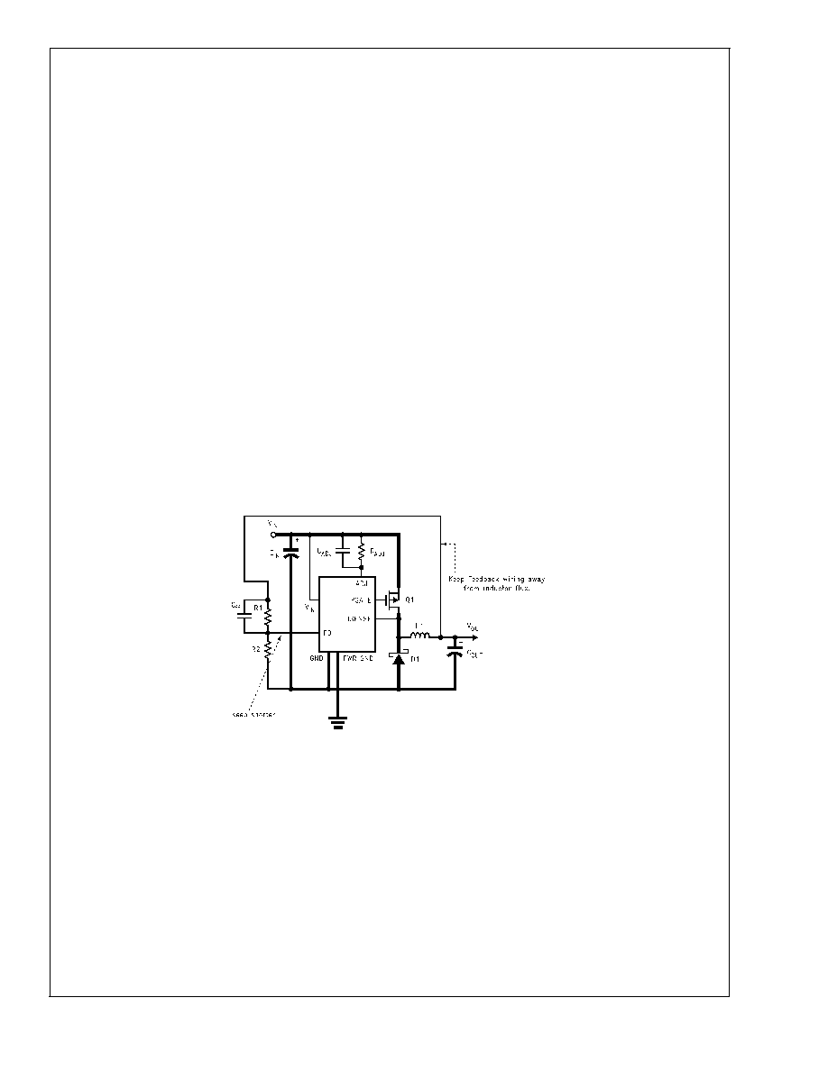
PCB Layout
The PC board layout is very important in all switching regu-
lator designs. Poor layout can cause switching noise into the
feedback signal and general EMI problems. For minimal
inductance, the wires indicated by heavy lines should be as
wide and short as possible. Keep the ground pin of the input
capacitor as close as possible to the anode of the diode. This
path carries a large AC current. The switching node, the
node with the diode cathode, inductor, and FET drain, should
be kept short. This node is one of the main sources for
radiated EMI since it is an AC voltage at the switching
frequency. It is always good practice to use a ground plane in
the design, particularly at high currents. The gate pin of the
external PFET should be located close to the PGATE pin.
However, if a very small FET is used, a resistor may be
required between PGATE and the gate of the FET to reduce
high frequency ringing.
The feedback voltage signal line can be sensitive to noise.
Make sure to avoid inductive coupling to the inductor or the
switching node.
20034628
FIGURE 6. Typical PCB Layout Schematic (3.3V output)
LM3485
www.national.com
13
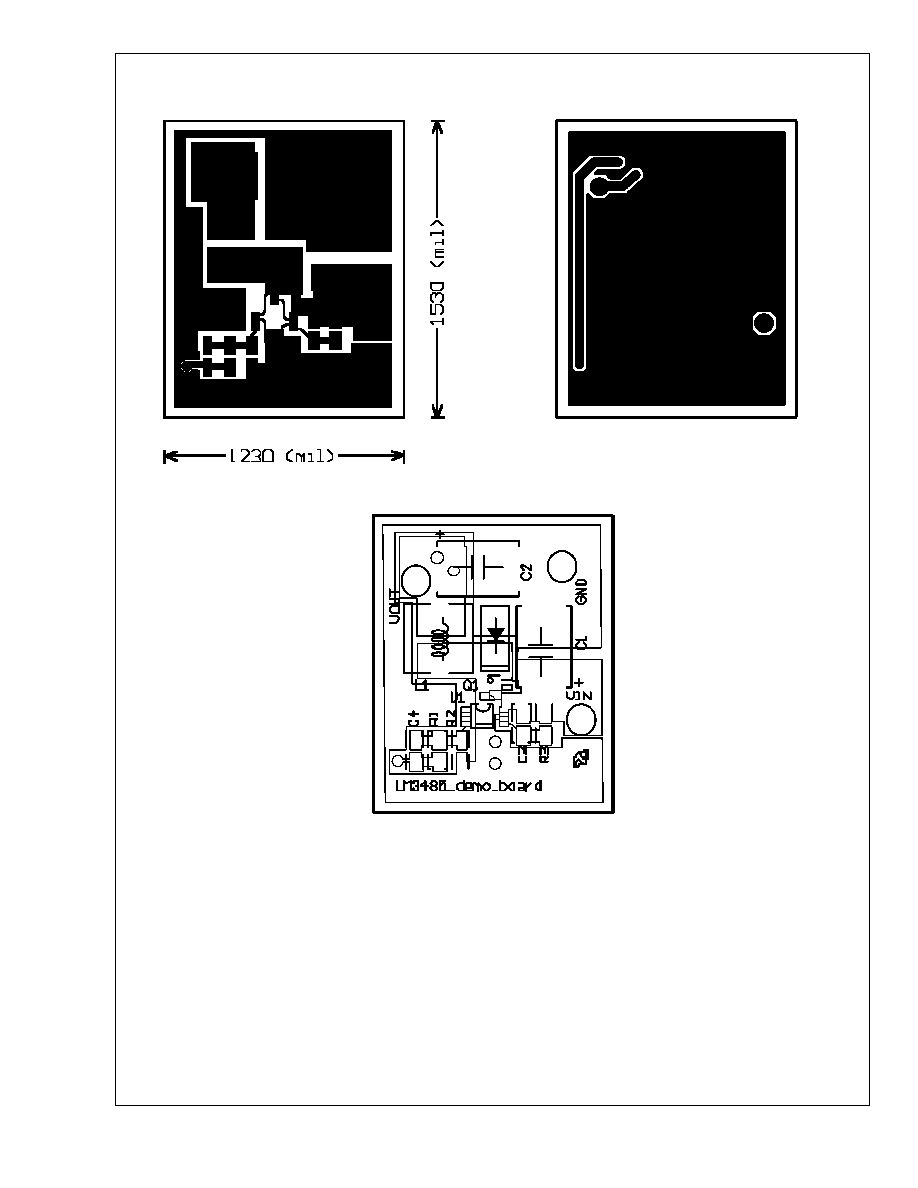
PCB Layout
(Continued)
20034642
Top Layer
20034644
Bottom Layer
20034641
Silk Screen
C1: C
IN
22µF/35V EEJL1VD226R (Panasonic)
C2: C
OUT
100µF/6.3V 6TPC100M (Sanyo)
C3: C
ADJ
1nF Ceramic Chip Capacitor
C4: C
FF
100pF Ceramic Chip Capacitor
D1: 1A/40V MBRS140T3 (On Semiconductor)
L1: 22µH :QH66SN220M01L (Murata)
Q1: FDC5614P (Fairchild)
R1: 33K
Chip Resistor
R2: 20K
Chip Resistor
R3: R
ADJ
24K
Chip Resistor
FIGURE 7. Typical PCB Layout (3.3V Output)
LM3485
www.national.com
14
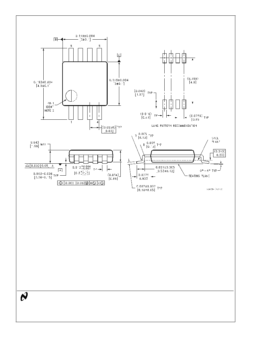
Physical Dimensions
inches (millimeters)
unless otherwise noted
8 Lead Plastic MSOP-8
NS package Number MUA08A
LIFE SUPPORT POLICY
NATIONAL'S PRODUCTS ARE NOT AUTHORIZED FOR USE AS CRITICAL COMPONENTS IN LIFE SUPPORT
DEVICES OR SYSTEMS WITHOUT THE EXPRESS WRITTEN APPROVAL OF THE PRESIDENT AND GENERAL
COUNSEL OF NATIONAL SEMICONDUCTOR CORPORATION. As used herein:
1. Life support devices or systems are devices or
systems which, (a) are intended for surgical implant
into the body, or (b) support or sustain life, and
whose failure to perform when properly used in
accordance with instructions for use provided in the
labeling, can be reasonably expected to result in a
significant injury to the user.
2. A critical component is any component of a life
support device or system whose failure to perform
can be reasonably expected to cause the failure of
the life support device or system, or to affect its
safety or effectiveness.
National Semiconductor
Corporation
Americas
Email: support@nsc.com
National Semiconductor
Europe
Fax: +49 (0) 180-530 85 86
Email: europe.support@nsc.com
Deutsch Tel: +49 (0) 69 9508 6208
English
Tel: +44 (0) 870 24 0 2171
FranÁais Tel: +33 (0) 1 41 91 8790
National Semiconductor
Asia Pacific Customer
Response Group
Tel: 65-2544466
Fax: 65-2504466
Email: ap.support@nsc.com
National Semiconductor
Japan Ltd.
Tel: 81-3-5639-7560
Fax: 81-3-5639-7507
www.national.com
LM3485
Hysteretic
PFET
Buck
Controller
National does not assume any responsibility for use of any circuitry described, no circuit patent licenses are implied and National reserves the right at any time without notice to change said circuitry and specifications.