LM3485
Hysteretic PFET Buck Controller
General Description
The LM3485 is a high efficiency PFET switching regulator
controller that a system designer can use to quickly and
easily develop a small, low cost, switching buck regulator for
a wide range of applications. The use of a hysteretic control
scheme provides for simple design without any control loop
stability concerns using a wide variety of external compo-
nents. The PFET architecture also allows for low component
count as well as ultra-low dropout operation. Another benefit
is high efficiency operation at light loads without an increase
in output ripple. Current limit protection circuit is provided by
measuring the voltage across the PFET's R
DSON
thus elimi-
nating a costly sense resistor. The current limit can be ad-
justed allowing for designs at various output currents and
costs.
Features
n
Easy to use control methodology
n
No control loop compensation required
n
4.5V to 35V wide input range
n
1.242V to V
IN
adjustable output range
n
High Efficiency 93%
n
±
1.3% (
±
2% over temp) internal reference
n
100% duty cycle
n
Maximum operating frequency
>
1MHz
n
Current limit protection
n
MSOP-8
Applications
n
Set-Top Box
n
DSL/Cable Modem
n
PC/IA
n
Auto PC
n
TFT Monitor
n
Battery Powered Portable Applications
n
Distributed Power Systems
n
Always On Power
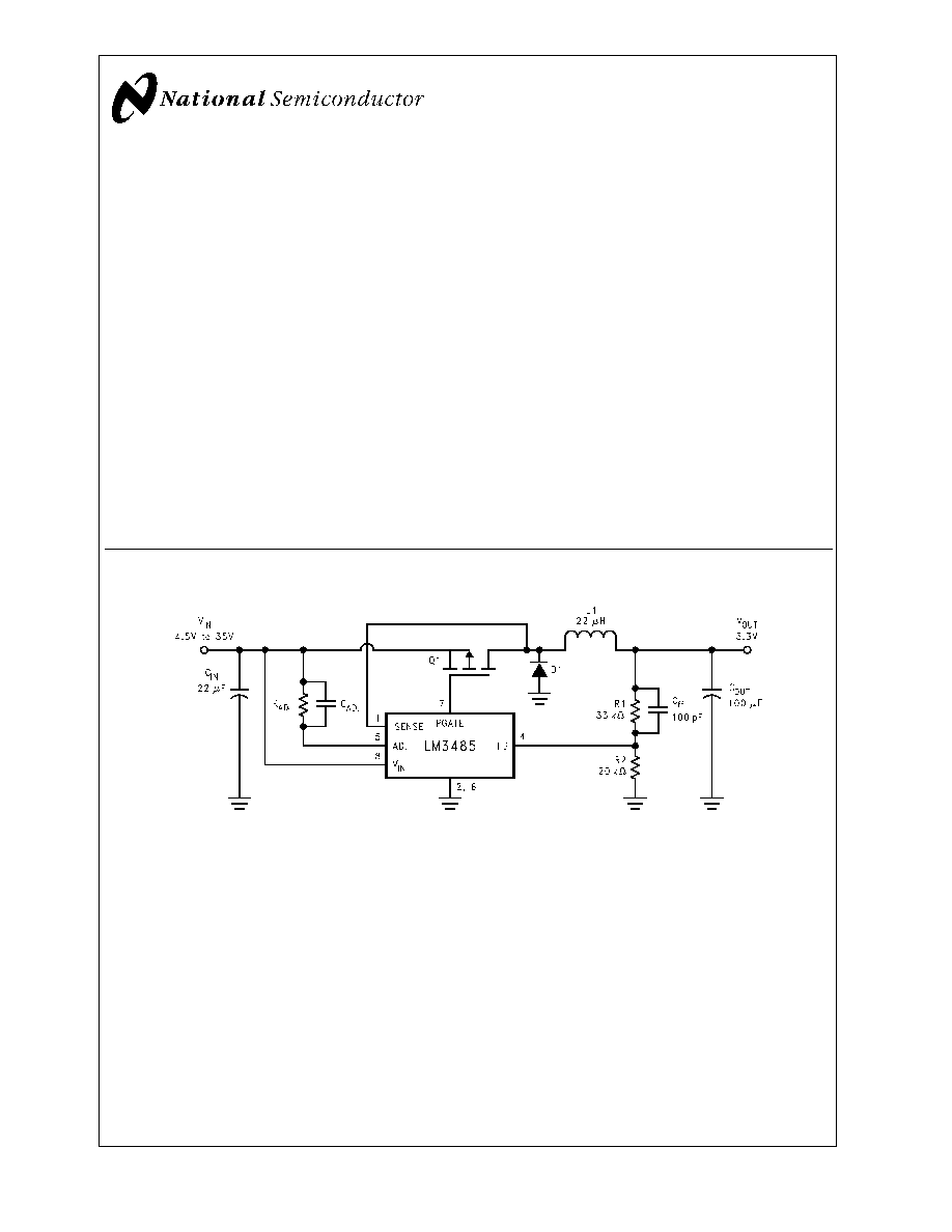
Typical Application Circuit
20034608
May 2002
LM3485
Hysteretic
PFET
Buck
Controller
© 2002 National Semiconductor Corporation
DS200346
www.national.com
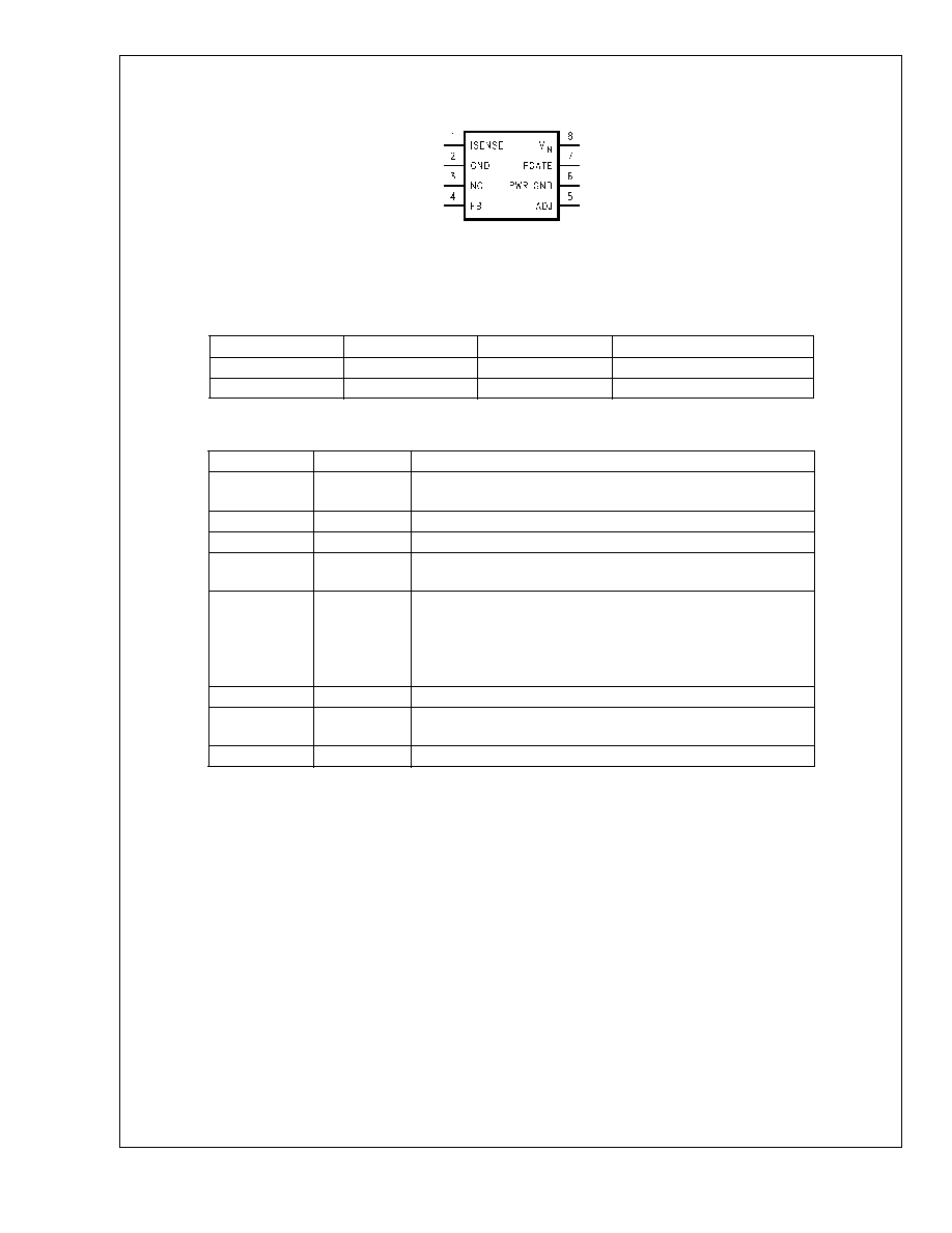
Connection Diagram
Top View
20034609
8 Lead Plastic MSOP-8
NS package Number MUA08A
Package Marking and Ordering Information
Order Number
Package Type
Package Marking
Supplied As:
LM3485MM
MSOP-8
S29B
1000 units on Tape and Reel
LM3485MMX
MSOP-8
S29B
3500 units on Tape and Reel
Pin Description
Pin Name
Pin Number
Description
ISENSE
1
The current sense input pin. This pin should be connected to Drain
node of the external PFET.
GND
2
Signal ground.
NC
3
No connection.
FB
4
The feedback input. Connect the FB to a resistor voltage divider
between the output and GND for an adjustable output voltage.
ADJ
5
Current limit threshold adjustment. It connects to an internal 5.5µA
current source. A resistor is connected between this pin and the
input Power Supply. The voltage across this resistor is compared
with the V
DS
of the external PFET to determine if an over-current
condition has occurred.
PWR GND
6
Power ground.
PGATE
7
Gate Drive output for the external PFET. PGATE swings between
V
IN
and V
IN
-5V.
VIN
8
Power supply input pin.
LM3485
www.national.com
2
Absolute Maximum Ratings
(Note 1)
If Military/Aerospace specified devices are required,
please contact the National Semiconductor Sales Office/
Distributors for availability and specifications.
VIN Voltage
-0.3V to 36V
PGATE Voltage
-0.3V to 36V
FB Voltage
-0.3V to 5V
ISENSE Voltage
-1.0V to 36V
ADJ Voltage
-0.3V to 36V
Maximum Junction Temp.
150∞C
Power Dissipation
417mW
@
T
A
=
25∞C
ESD Susceptibilty
Human Body Model (Note 3)
2kV
Lead Temperature
Vapor Phase (60 sec.)
Infared (15 sec.)
215∞C
220∞C
Storage Temperature
-65∞C to 150∞C
Operating Ratings
(Note 1)
Supply Voltage
4.5V to 35V
Operating Junction
Temperature
-40∞C to +125∞C
Electrical Characteristics
Specifications in Standard type face are for T
J
= 25∞C, and in bold type face apply over the full Operating Temperature
Range (T
J
= -40∞C to +125∞C). Unless otherwise specified, V
IN
= 12V, V
ISNS
= V
IN
- 1V, and V
ADJ
= V
IN
- 1.1V. Datasheet
min/max specification limits are guaranteed by design, test, or statistical analysis.
Symbol
Parameter
Conditions
Min
(Note 4)
Typ
(Note 5)
Max
(Note 4)
Unit
I
Q
Quiescent Current at
ground pin
FB = 1.5V
(Not Switching)
250
400
µA
V
FB
Feedback Voltage
(Note 6)
1.226
1.217
1.242
1.258
1.267
V
V
HYST
Comparator
Hysteresis
10
14
15
20
mV
V
CL
(Note 7)
Current limit
comparator trip
voltage
R
ADJ
= 20k
110
mV
R
ADJ
= 160k
880
V
CL_OFFSET
Current limit
comparator offset
V
FB
= 1.5V
-20
0
+20
mV
I
CL_ADJ
Current limit ADJ
current source
V
FB
= 1.5V
3.0
5.5
7.0
µA
T
CL
Current limit one shot
off time
V
ADJ
= 11.5V
V
ISNS
= 11.0V
V
FB
= 1.0V
6
9
14
µs
R
PGATE
Driver resistance
Source
I
SOURCE
= 100mA
5.5
Sink
I
Sink
= 100mA
8.5
I
PGATE
Driver Output current
Source
V
IN
= 7V,
P
GATE
= 3.5V
0.44
A
Sink
V
IN
= 7V,
P
GATE
= 3.5V
0.32
V
PGATEMIN
Minimum driver
voltage
V
IN
= 4.5V
V
FB
= 1.0V
I
GATE
= 100µA sink
1.2
V
I
FB
FB pin Bias Current
(Note 8)
V
FB
= 1.0V
300
750
nA
T
ONMIN_NOR
Minimum on time in
normal operation
V
ISNS
= V
ADJ
+0.1V
C
load
on OUT =
1000pF
(Note 9)
100
ns
LM3485
www.national.com
3
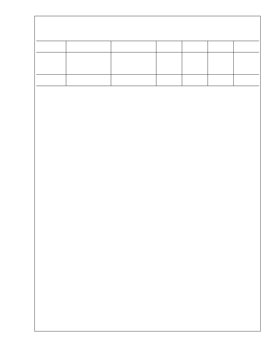
Electrical Characteristics
(Continued)
Specifications in Standard type face are for T
J
= 25∞C, and in bold type face apply over the full Operating Temperature
Range (T
J
= -40∞C to +125∞C). Unless otherwise specified, V
IN
= 12V, V
ISNS
= V
IN
- 1V, and V
ADJ
= V
IN
- 1.1V. Datasheet
min/max specification limits are guaranteed by design, test, or statistical analysis.
Symbol
Parameter
Conditions
Min
(Note 4)
Typ
(Note 5)
Max
(Note 4)
Unit
T
ONMIN_CL
Minimum on time in
current limit
V
ISNS
= V
ADJ
+0.1V
V
FB
= 1.0V C
load
on
OUT = 1000pF
(Note 9)
175
ns
%V
FB
/
V
IN
Feedback Voltage
Line Regulation
4.5
V
IN
35V
0.010
%/V
Note 1: Absolute maximum ratings are limits beyond which damage to the device may occur. Operating Ratings are conditions for which the device is intended to
be functional, but device parameter specifications may not be guaranteed. For guaranteed specifications and test conditions, see the Electrical Characteristics.
Note 2: The maximum allowable power dissipation is a function of the maximum junction temperature, T
J_MAX
, the junction-to-ambient thermal resistance,
JA
=
240∞C/W, and the ambient temperature, T
A
. The maximum allowable power dissipation at any ambient temperature is calculated using:
P
D_MAX
= (T
J_MAX
- T
A
)/
JA
. Exceeding the maximum allowable power dissipation will cause excessive die temperature.
Note 3: The human body model is a 100 pF capacitor discharged through a 1.5k
resistor into each pin.
Note 4: All limits are guaranteed at room temperature (standard type face) and at temperature extremes (bold type face). All room temperature limits are 100%
tested. All limits at temperature extremes are guaranteed via correlation using standard Statistical Quality Control (SQC) methods. All limits are used to calculate
Average Outgoing Quality Level (AOQL).
Note 5: Typical numbers are at 25∞C and represent the most likely norm.
Note 6: The V
FB
is the trip voltage at the FB pin when PGATE switches from high to low.
Note 7: V
CL
= I
CL_ADJ
*
R
ADJ
Note 8: Bias current flows out from the FB pin.
Note 9: A 1000pF capacitor is connected between V
IN
and PGATE.
LM3485
www.national.com
4
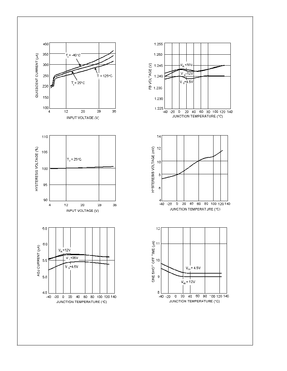
Typical Performance Characteristics
Unless otherwise specified, T
J
= 25∞C
Quiescent Current vs Input Voltage
(FB = 1.5V)
Feedback Voltage vs Temperature
20034601
20034607
Hysteresis Voltage vs Input Voltage
Hysteresis Voltage vs Temperature
20034605
20034606
Current Limit ADJ Current vs Temperature
Current Limit One Shot OFF Time vs. Temperature
20034602
20034604
LM3485
www.national.com
5