 | –≠–ª–µ–∫—Ç—Ä–æ–Ω–Ω—ã–π –∫–æ–º–ø–æ–Ω–µ–Ω—Ç: LM3489 | –°–∫–∞—á–∞—Ç—å:  PDF PDF  ZIP ZIP |
LM3489
Hysteretic PFET Buck Controller with Enable Pin
General Description
The LM3489 is a high efficiency PFET switching regulator
controller that can be used to quickly and easily develop a
small, cost effective, switching buck regulator for a wide
range of applications. The hysteretic control architecture
provides for simple design without any control loop stability
concerns using a wide variety of external components. The
PFET architecture also allows for low component count as
well as ultra-low dropout, 100% duty cycle operation. An-
other benefit is high efficiency operation at light loads without
an increase in output ripple. A dedicated Enable Pin provides
a shutdown mode drawing only 7µA. Leaving the Enable Pin
unconnected defaults to on.
Current limit protection can be implemented by measuring
the voltage across the PFET's R
DS(ON)
, thus eliminating the
need for a sense resistor. A sense resistor may be used to
improve current limit accuracy if desired. The cycle-by-cycle
current limit can be adjusted with a single resistor, ensuring
safe operation over a range of output currents.
Features
n
Easy to use control methodology
n
No control loop compensation required
n
Wide 4.5V to 35V input range
n
1.239V to V
IN
adjustable output range
n
High efficiency 93%
n
±
1.3% (
±
2% over temp) internal reference
n
100% duty cycle operation
n
Maximum operation frequency
>
1MHz
n
Current limit protection
n
Dedicated enable pin (on if unconnected)
n
Shutdown mode draws only 7µA supply current
n
MSOP-8
Applications
n
Set-Top Box
n
DSL/Cable Modem
n
PC/IA
n
Auto PC
n
TFT Monitor
n
Battery Powered Portable Applications
n
Distributed Power Systems
n
Always On Power
n
High Power LED Driver
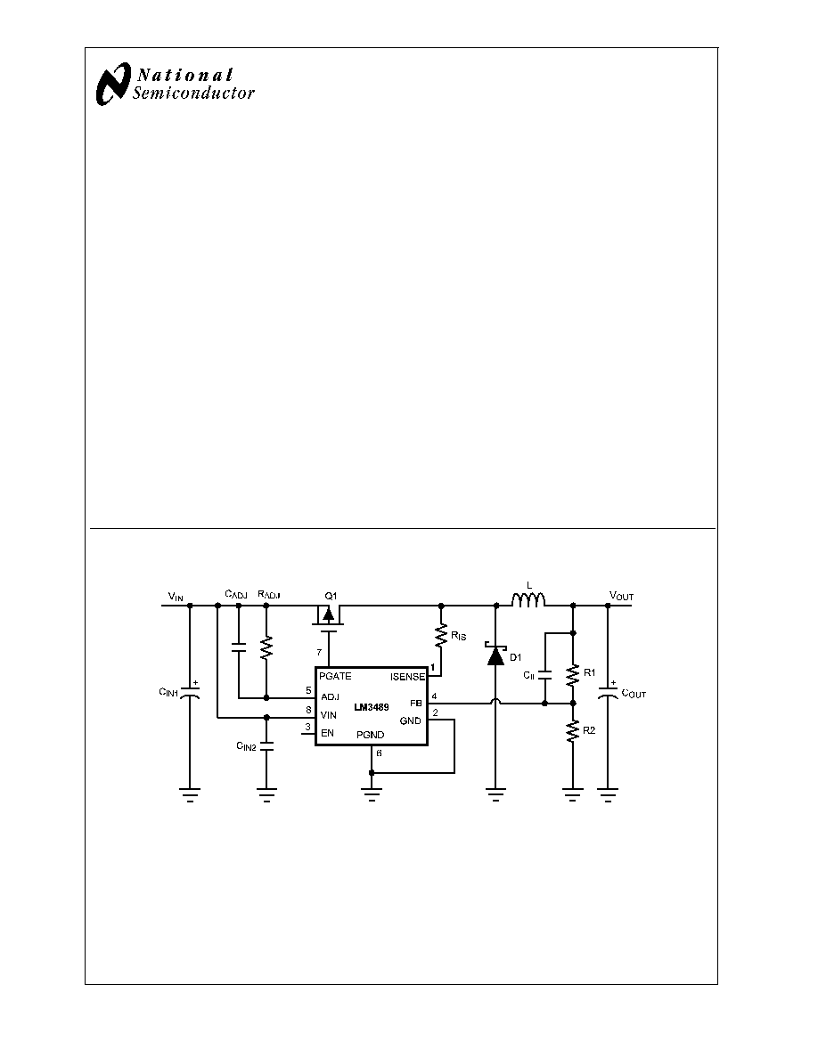
Typical Application Circuit
20186908
May 2006
LM3489
Hysteretic
PFET
Buck
Controller
with
Enable
Pin
© 2006 National Semiconductor Corporation
DS201869
www.national.com
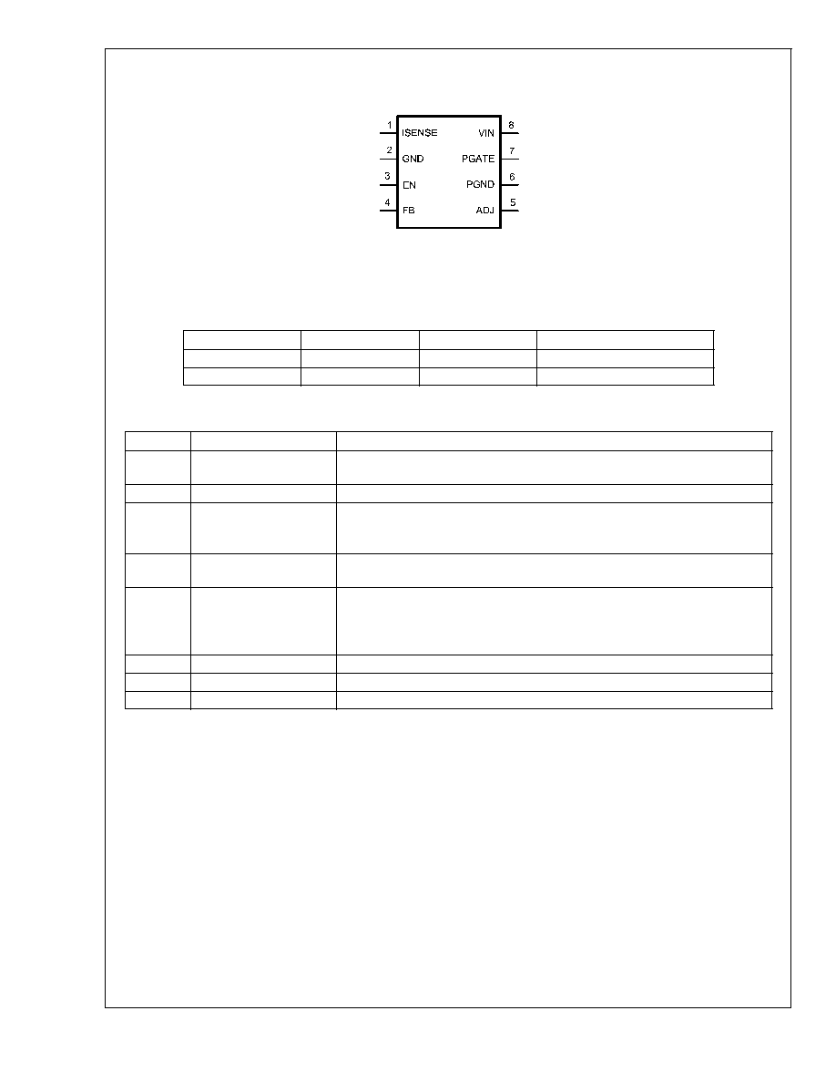
Connection Diagram
Top View
20186909
8 Lead Plastic MSOP-8
NS package Number MUA08A
Package Marking and Ordering Information
Order Number
Package Type
Package Marking
Supplied As:
LM3489MM
MSOP-8
SKSB
1000 units on Tape and Reel
LM3489MMX
MSOP-8
SKSB
3500 units on Tape and Reel
Pin Descriptions
Pin #
Name
Description
1
ISENSE
The current sense input pin. This pin should be connected to the PFET drain
terminal directly or through a series resistor up to 600 ohm for 28V
>
Vin
>
35V.
2
GND
Signal ground.
3
EN
Enable pin. Connect EN pin to ground to shutdown the part or float to enable
operation (Internally pulled high). This pin can also be used to perform UVLO
function.
4
FB
The feedback input. Connect the FB to a resistor voltage divider between the
output and GND for an adjustable output voltage.
5
ADJ
Current limit threshold adjustment. Connected to an internal 5.5µA current source.
A resistor is connected between this pin and VIN. The voltage across this resistor
is compared with the ISENSE pin voltage to determine if an over-current condition
has occurred.
6
PGND
Power ground.
7
PGATE
Gate Drive output for the external PFET. PGATE swings between VIN and VIN-5V.
8
VIN
Power supply input pin.
LM3489
www.national.com
2

Absolute Maximum Ratings
(Note 1)
If Military/Aerospace specified devices are required,
please contact the National Semiconductor Sales Office/
Distributors for availability and specifications.
VIN Voltage
-0.3V to 36V
PGATE Voltage
-0.3V to 36V
FB Voltage
-0.3V to 5V
ISENSE Voltage
-1.0V to 36V
-1V (
<
100ns)
ADJ Voltage
-0.3V to 36V
EN Voltage (Note 3)
-0.3V to 6V
Maximum Junction Temp.
150∞C
Power Dissipation, T
A
= 25∞C
(Note 2)
417mW
ESD Susceptibilty (Note 4)
Human Body Model
2kV
Lead Temperature
Vapor Phase (60 sec.)
Infared (15 sec.)
215∞C
220∞C
Storage Temperature
-65∞C to 150∞C
Operating Ratings
(Note 1)
Supply Voltage Range (V
IN
)
4.5V to 35V
EN Voltage (max.) (Note 3)
5.5V
Operating Junction Temperature
(T
J
)
-40∞C to +125∞C
Electrical Characteristics
(Note 5)
,
(Note 6)
Specifications in Standard type face are for T
J
= 25∞C, and in
bold type face apply over the full Operating Temperature Range (T
J
= -40∞C to +125∞C). Unless otherwise specified, V
IN
=
12V, V
ISNS
= V
IN
- 1V, and V
ADJ
= V
IN
- 1.1V. Datasheet min/max specification limits are guaranteed by design, test, or sta-
tistical analysis.
Symbol
Parameter
Conditions
Min
Typ
Max
Units
I
SHDN
Shutdown input supply current
EN = 0V
7
15
µA
V
EN
Enable threshold voltage
Enable rising
1.15
1.5
1.85
V
V
EN_HYST
Enable threshold hysteresis
130
mV
I
Q
Quiescent Current at ground pin
FB = 1.5V (Not Switching)
280
400
µA
V
FB
(Note 7)
Feedback Voltage
1.223
1.214
1.239
1.255
1.264
V
V
HYST
Comparator Hysteresis
10
14
15
20
mV
V
CL_OFFSET
Current limit comparator offset
V
FB
= 1.0V
-20
0
+20
mV
I
CL_ADJ
Current limit ADJ current source
V
FB
= 1.5V
3.0
5.5
7.0
µA
T
CL
Current limit one shot off time
V
ADJ
= 11.5V
V
ISNS
= 11.0V
V
FB
= 1.0V
6
9
14
µs
R
PGATE
Driver resistance
Source
I
SOURCE
= 100mA
5.5
Sink
I
SINK
= 100mA
8.5
I
PGATE
Driver Output current
Source
V
IN
= 7V, PGATE = 3.5V
0.44
A
Sink
VIN = 7V, PGATE = 3.5V
0.1
I
FB
(Note 9)
FB pin Bias Current
V
FB
= 1.0V
300
750
nA
T
ONMIN_NOR
Minimum on time in normal
operation
V
ISNS
= V
ADJ
+ 0.1V
Cload on OUT = 1000pF (Note 10)
100
ns
T
ONMIN_CL
Minimum on time in current limit
V
ISNS
= V
ADJ
- 0.1V
VFB = 1.0V
Cload on OUT = 1000pF (Note 10)
200
ns
%V
FB
/
V
IN
Feedback Voltage Line Regulation
4.5
V
IN
35V
0.01
%/V
LM3489
www.national.com
3

Electrical Characteristics
(Note 5)
,
(Note 6) Specifications in Standard type face are for T
J
= 25∞C, and in
bold type face apply over the full Operating Temperature Range (T
J
= -40∞C to +125∞C). Unless otherwise specified, V
IN
=
12V, V
ISNS
= V
IN
- 1V, and V
ADJ
= V
IN
- 1.1V. Datasheet min/max specification limits are guaranteed by design, test, or
statistical analysis. (Continued)
Note 1: Absolute maximum ratings are limits beyond which damage to the device may occur. Operating Ratings are conditions for which the device is intended to
be functional, but device parameter specifications may not be guaranteed. For guaranteed specifications and test conditions, see the Electrical Characteristics.
Note 2: The maximum allowable power dissipation is a function of the maximum junction temperature, T
J_MAX
, the junction-to-ambient thermal resistance,
JA
=
240∞C/W, and the ambient temperature, T
A
. The maximum allowable power dissipation at any ambient temperature is calculated using:
P
D_MAX
= (T
J_MAX
- T
A
)/
JA
. Exceeding the maximum allowable power dissipation will cause excessive die temperature.
Note 3: This pin is internally pulled high and clamped at 8V typical. The absolute maximum and operating maximum rating specifies the input level allowed for an
external voltage source applied to this pin without triggering the internal clamp with margin.
Note 4: The human body model is a 100 pF capacitor discharged through a 1.5k
resistor into each pin. The machine model is a 200pF capacitor discharged
directly into each pin. MIL-STD-883 3015.7
Note 5: All limits are guaranteed at room temperature (standard type face) and at temperature extremes (bold type face). All room temperature limits are 100%
tested. All limits at temperature extremes are guaranteed via correlation using standard Statistical Quality Control (SQC) methods. All limits are used to calculate
Average Outgoing Quality Level (AOQL).
Note 6: Typical numbers are at 25∞C and represent the most likely norm.
Note 7: The V
FB
is the trip voltage at the FB pin when PGATE switches from high to low.
Note 8: V
CL
= I
CL_ADJ
* R
ADJ
Note 9: Bias current flows out from the FB pin.
Note 10: A 1000pF capacitor is connected between V
IN
and PGATE.
LM3489
www.national.com
4
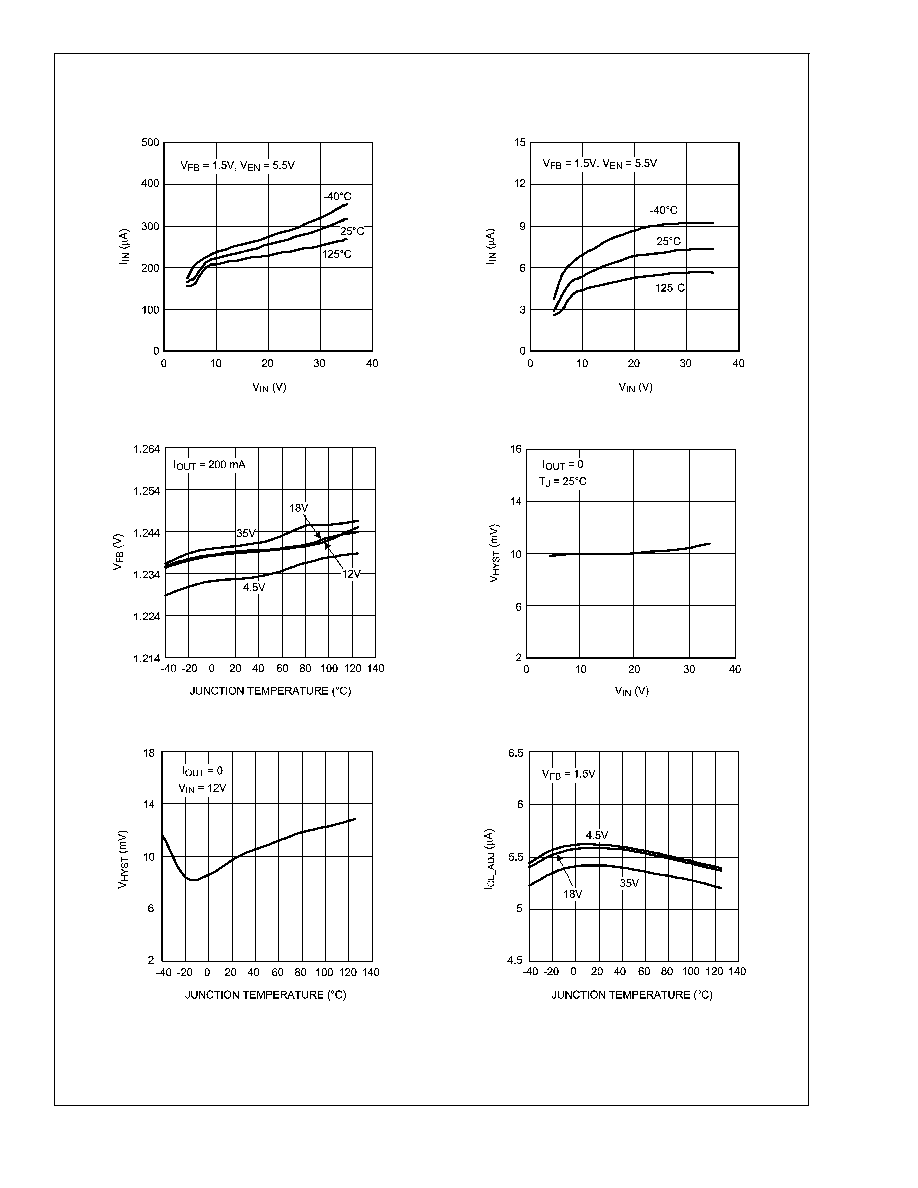
Typical Performance Characteristics
All curves taken at VIN = 12V with configuration in typical ap-
plication circuit shown in Application Information section of this datasheet. T
J
= 25∞C, unless otherwise specified.
Quiescent Current vs Input Voltage
Shutdown Current vs Input Voltage
20186901
20186902
Feedback Voltage vs Temperature
Feedback Voltage Hysteresis vs Input Voltage
20186903
20186904
Feedback Voltage Hysteresis vs Temperature
Current Limit ADJ Current vs Temperature
20186905
20186906
LM3489
www.national.com
5