LM3490
100 mA, SOT-23, Quasi Low-Dropout Linear Voltage
Regulator with Logic-Controlled ON/OFF
General Description
The LM3490 is an integrated linear voltage regulator. It fea-
tures operation from an input as high as 30V and a guaran-
teed maximum dropout of 1.2V at the full 100 mA load. Stan-
dard packaging for the LM3490 is the 5-lead SOT-23
package. A logic-controlled ON/OFF feature makes the
LM3490 ideal for powering subsystems ON and OFF as
needed.
The 5, 12, and 15V members of the LM3490 series are in-
tended as tiny alternatives to industry standard LM78LXX
series and similar devices. The 1.2V quasi low dropout of
LM3490 series devices makes them a nice fit in many appli-
cations where the 2 to 2.5V dropout of LM78LXX series de-
vices precludes their (LM78LXX series devices) use.
The LM3490 series features a 3.3V member. The SOT pack-
aging and quasi low dropout features of the LM3490 series
converge in this device to provide a very nice, very tiny 3.3V,
100 mA bias supply that regulates directly off the system
5V
±
5% power supply.
Key Specifications
n
30V maximum input for operation
n
1.2V guaranteed maximum dropout over full load and
temperature ranges
n
100 mA guaranteed load current
n
±
5% guaranteed output voltage tolerance over full load
and temperature ranges
n
-40 to +125∞C junction temperature range for operation
Features
n
3.3, 5, 12, and 15V versions available
n
Logic-controlled ON/OFF
n
Packaged in the tiny 5-lead SOT-23 package
Applications
n
Tiny alternative to LM78LXX series and similar devices
n
Tiny 5V
±
5% to 3.3V, 100 mA converter
n
Post regulator for switching DC/DC converter
n
Bias supply for analog circuits
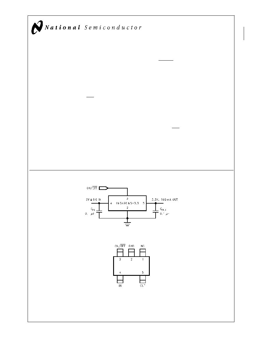
Typical Application Circuit
Connection Diagram
DS100071-2
DS100071-1
Top View
SOT-23 Package
5-Lead, Molded-Plastic Small-Outline Transistor (SOT) Package
Package Code MF05A(Note 1)
July 2000
LM3490
100
mA,
SOT
-23,
Quasi
Low-Dropout
Linear
V
oltage
Regulator
with
Logic-Controlled
ON/OFF
© 2000 National Semiconductor Corporation
DS100071
www.national.com
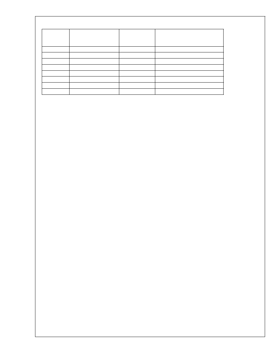
Ordering Information
Output
Voltage
(V)
Order
Number
(Note 2)
Package
Marking
(Note 3)
Comments
3.3
LM3490IM5-3.3
L78B
1000 Units on Tape and Reel
3.3
LM3490IM5X-3.3
L78B
3000 Units on Tape and Reel
5
LM3490IM5-5.0
L79B
1000 Units on Tape and Reel
5
LM3490IM5X-5.0
L79B
3000 Units on Tape and Reel
12
LM3490IM5-12
L80B
1000 Units on Tape and Reel
12
LM3490IM5X-12
L80B
3000 Units on Tape and Reel
15
LM3490IM5-15
L81B
1000 Units on Tape and Reel
15
LM3490IM5X-15
L81B
3000 Units on Tape and Reel
LM3490
www.national.com
2
Absolute Maximum Ratings
(Note 4)
If Military/Aerospace specified devices are required,
please contact the National Semiconductor Sales Office/
Distributors for availability and specifications.
Input Voltage (IN to GND)
35V
Voltage ON/OFF to GND
5.5V
Power Dissipation (Note 5)
400 mW
Junction Temp. (T
J
) (Note 5)
+150∞C
Ambient Storage Temp.
-65 to +150∞C
Soldering Time, Temp. (Note 6)
Wave
Infrared
Vapor Phase
4sec., 260∞C
10sec., 240∞C
75sec., 219∞C
ESD (Note 7)
ON/OFF
All Other Pins
1.0kV
2.0kV
Operating Ratings
(Note 4)
Maximum Input Voltage (IN to GND)
30V
Voltage ON/OFF to GND
0 to 5V
Junction Temperature (T
J
)
-40 to +125∞C
Maximum Power Dissipation (Note 8)
300 mW
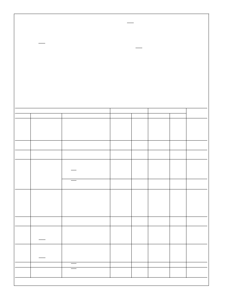
Electrical Characteristics
LM3490-3.3, LM3490-5.0
V
IN
= V
NOM
+ 1.5V unless otherwise noted. Typicals and limits appearing in normal type apply for T
A
= T
J
= 25∞C. Limits ap-
pearing in boldface type apply over the entire junction temperature range for operation, -40 to +125∞C. (Notes 9, 10, 11)
Nominal Output Voltage (V
NOM
)
3.3V
5.0V
Units
Symbol
Parameter
Conditions
Typical
Limit
Typical
Limit
V
OUT
Output Voltage
1 mA
I
OUT
100 mA
3.30
3.17
3.14
3.43
3.46
5.00
4.80
4.75
5.20
5.25
V
V(min)
V(min)
V(max)
V(max)
V
OUT
Line Regulation
V
NOM
+ 1.5V
V
IN
30V,
I
OUT
= 1 mA
7
25
9
25
mV
mV(max)
V
OUT
Load Regulation
10 mA
I
OUT
100 mA
15
40
15
40
mV
mV(max)
I
GND
Ground Pin
Current
V
NOM
+ 1.5V
V
IN
30V,
No Load
V
ON/OFF
= 5V
2
2
mA
4
4
mA(max)
V
ON/OFF
= 0V
0.1
0.1
µA
5
5
µA(max)
V
IN
-
V
OUT
Dropout Voltage
I
OUT
= 10 mA
0.7
0.9
1.0
0.7
0.9
1.0
V
V(max)
V(max)
I
OUT
= 100 mA
0.9
1.1
1.2
0.9
1.1
1.2
V
V(max)
V(max)
e
n
Output Noise
Voltage
V
IN
= 10V,
Bandwidth: 10 Hz to 100 kHz
100
150
µV
rms
V
IL
Maximum Low
Level Input
Voltage at
ON/OFF
0.2
0.2
V(max)
V
IH
Minimum High
Level Input
Voltage at
ON/OFF
2.0
2.0
V(min)
I
IL
V
ON/OFF
= 0V
-1
-1
µA(max)
I
IH
V
ON/OFF
= 5V
1
1
µA
20
20
µA(max)
LM3490
www.national.com
3
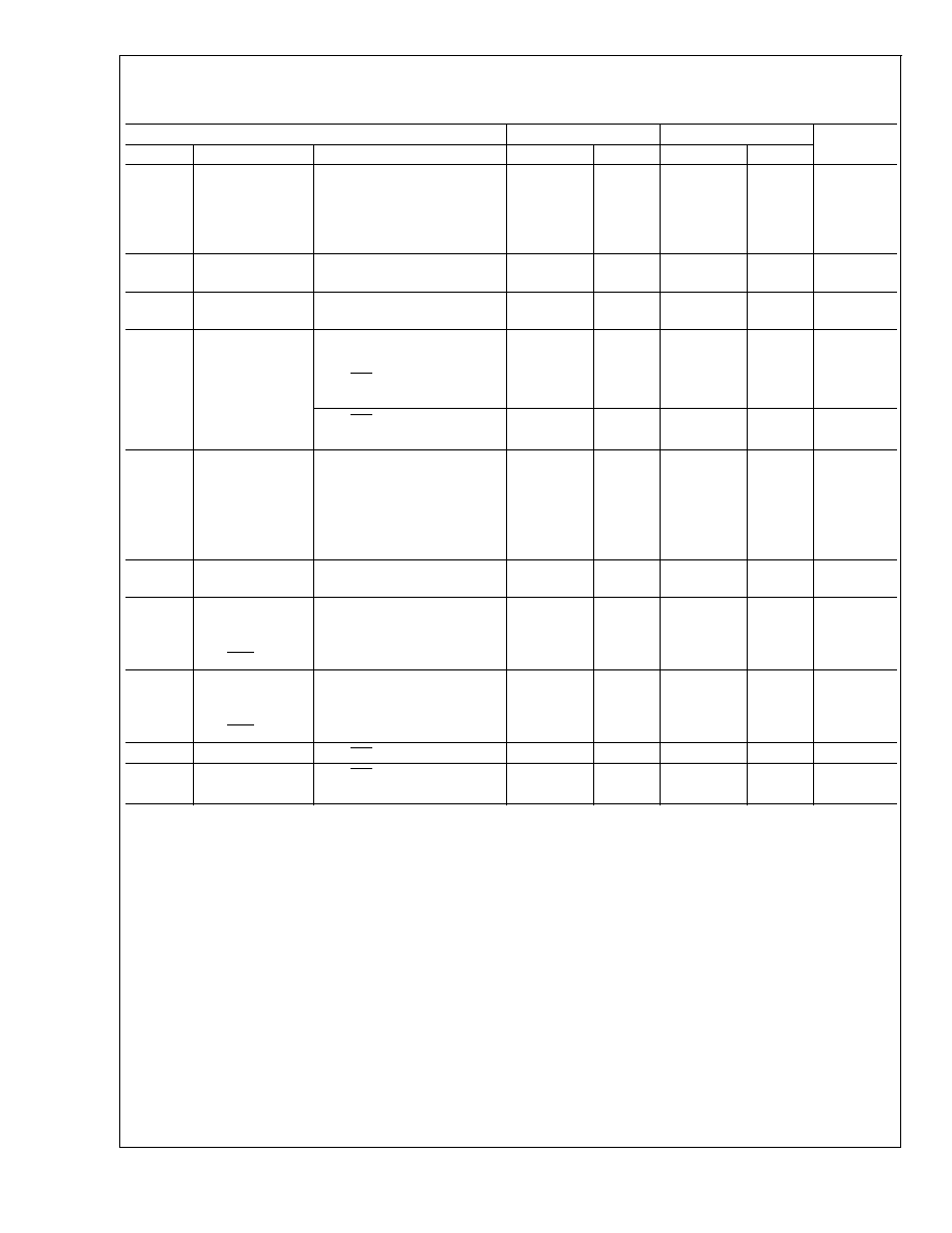
LM3490-12, LM3490-15
V
IN
= V
NOM
+ 1.5V unless otherwise noted. Typicals and limits appearing in normal type apply for T
A
= T
J
= 25∞C. Limits ap-
pearing in boldface type apply over the entire junction temperature range for operation, -40 to +125∞C. (Notes 9, 10, 11)
Nominal Output Voltage (V
NOM
)
12V
15V
Units
Symbol
Parameter
Conditions
Typical
Limit
Typical
Limit
V
OUT
Output Voltage
1 mA
I
OUT
100 mA
12.00
11.52
11.40
12.48
12.60
15.00
14.40
14.25
15.60
15.75
V
V(min)
V(min)
V(max)
V(max)
V
OUT
Line Regulation
V
NOM
+ 1.5V
V
IN
30V,
I
OUT
= 1 mA
14
40
16
40
mV
mV(max)
V
OUT
Load Regulation
10 mA
I
OUT
100 mA
36
60
45
75
mV
mV(max)
I
GND
Ground Pin
Current
V
NOM
+ 1.5V
V
IN
30V,
No Load
V
ON/OFF
= 5V
2
2
mA
4
4
mA(max)
V
ON/OFF
= 0V
0.1
0.1
µA
5
5
µA(max)
V
IN
-
V
OUT
Dropout Voltage
I
OUT
= 10 mA
0.7
0.9
1.0
0.7
0.9
1.0
V
V(max)
V(max)
I
OUT
= 100 mA
0.9
1.1
1.2
0.9
1.1
1.2
V
V(max)
V(max)
e
n
Output Noise
Voltage
V
IN
= 10V,
Bandwidth: 10 Hz to 100 kHz
360
450
µV
rms
V
IL
Maximum Low
Level Input
Voltage at
ON/OFF
0.2
0.2
V(max)
V
IH
Minimum High
Level Input
Voltage at
ON/OFF
2.0
2.0
V(min)
I
IL
V
ON/OFF
= 0V
-1
-1
µA(max)
I
IH
V
ON/OFF
= 5V
1
1
µA
20
20
µA(max)
Note 1: The package code MA05B is internal to National Semiconductor Corporation and indicates a specific version of the SOT-23 package and associated me-
chanical drawings.
Note 2: The suffix "I" indicates the junction temperature range for operation is the industrial temperature range, -40 to +125∞C. The suffix "M5" indicates the die is
packaged in the 5-lead SOT-23 package. The suffix "X" indicates the devices will be supplied in blocks of 3k units as opposed to blocks of 250 units.
Note 3: Because the entire part number does not fit on the SOT-23 package, the SOT-23 package is marked with this code instead of the part number.
Note 4: Absolute Maximum Ratings are limits beyond which damage to the device may occur. Operating Ratings are conditions under which operation of the device
is guaranteed. Operating Ratings do not imply guaranteed performance limits. For guaranteed performance limits and associated test conditions, see the Electrical
Characteristics tables.
Note 5: The Absolute Maximum power dissipation depends on the ambient temperature and can be calculated using P = (T
J
- T
A
)/
JA
where T
J
is the junction tem-
perature, T
A
is the ambient temperature, and
JA
is the junction-to-ambient thermal resistance. The 400 mW rating results from substituting the Absolute Maximum
junction temperature, 150∞C, for T
J
, 50∞C for T
A
, and 250∞C/W for
JA
. More power can be safely dissipated at lower ambient temperatures. Less power can be safely
dissipated at higher ambient temperatures. The Absolute Maximum power dissipation can be increased by 4 mW for each ∞C below 50∞C ambient. It must be derated
by 4 mW for each ∞C above 50∞C ambient. A
JA
of 250∞C/W represents the worst-case condition of no heat sinking of the 5-lead plastic SOT-23 package. Heat sinking
enables the safe dissipation of more power. The LM3490 actively limits its junction temperature to about 150∞C.
Note 6: Times shown are dwell times. Temperatures shown are dwell temperatures. For detailed information on soldering plastic small-outline packages, refer to the
Packaging Databook
available from National Semiconductor Corporation.
Note 7: For testing purposes, ESD was applied using the human-body model, a 100 pF capacitor discharged through a 1.5 k
resistor.
Note 8: As with the Absolute Maximum power dissipation, the maximum power dissipation for operation depends on the ambient temperature. The 300 mW rating
appearing under Operating Ratings results from substituting the maximum junction temperature for operation, 125∞C, for T
J
, 50∞C for T
A
, and 250∞C/W for
JA
in
P = (T
J
- T
A
)/
JA
. More power can be dissipated at lower ambient temperatures. Less power can be dissipated at higher ambient temperatures. The maximum power
dissipation for operation appearing under Operating Ratings can be increased by 4 mW for each ∞C below 50∞C ambient. It must be derated by 4 mW for each ∞C
above 50∞C ambient. A
JA
of 250∞C/W represents the worst-case condition of no heat sinking of the 5-lead plastic SOT-23 package. Heat sinking enables the dis-
sipation of more power during operation.
LM3490
www.national.com
4

LM3490-12, LM3490-15
(Continued)
Note 9: A typical is the center of characterization data taken with T
A
= T
J
= 25∞C. Typicals are not guaranteed.
Note 10: All limits are guaranteed. All electrical characteristics having room-temperature limits are tested during production with T
A
= T
J
= 25∞C. All hot and cold lim-
its are guaranteed by correlating the electrical characteristics to process and temperature variations and applying statistical process control.
Note 11: All voltages except dropout are with respect to the voltage at the GND pin.
LM3490
www.national.com
5